সূচিপত্র
- 1. পণ্যের সারসংক্ষেপ
- 1.1 মূল সুবিধা এবং লক্ষ্য বাজার
- 2. প্রযুক্তিগত পরামিতির গভীর বিশ্লেষণ
- 2.1 পরম সর্বোচ্চ রেটিং
- 2.2 অপটোইলেকট্রিক বৈশিষ্ট্য
- 3. গ্রেডিং সিস্টেমের ব্যাখ্যা
- 4. পারফরম্যান্স কার্ভ বিশ্লেষণ
- 4.1 ফরওয়ার্ড কারেন্ট এবং পরিবেষ্টিত তাপমাত্রার সম্পর্ক
- 4.2 বিকিরণ তীব্রতা এবং ফরওয়ার্ড কারেন্টের সম্পর্ক
- 4.3 বর্ণালী বণ্টন
- 4.4 আপেক্ষিক বিকিরণ তীব্রতা এবং কৌণিক সরণের সম্পর্ক
- 5. যান্ত্রিক এবং প্যাকেজিং তথ্য
- 5.1 প্যাকেজ মাত্রা চিত্র
- 5.2 পোলারিটি সনাক্তকরণ
- 6. সোল্ডারিং ও অ্যাসেম্বলি নির্দেশিকা
- 6.1 পিন গঠন
- 6.2 সংরক্ষণের শর্ত
- 6.3 ওয়েল্ডিং প্যারামিটার
- 6.4 পরিষ্কার
- 7. প্যাকেজিং এবং অর্ডার তথ্য
- 7.1 প্যাকেজিং স্পেসিফিকেশন
- 7.2 লেবেল ফরম্যাট স্পেসিফিকেশন
- 8. প্রয়োগের সুপারিশ
- 8.1 সাধারণ প্রয়োগের দৃশ্যাবলী
- 8.2 নকশা সংক্রান্ত বিবেচ্য বিষয়
- 9. প্রযুক্তিগত তুলনা ও পার্থক্য
- 10. সাধারণ প্রশ্নাবলী (প্রযুক্তিগত প্যারামিটার ভিত্তিক)
- 11. বাস্তব নকশা ও ব্যবহারের উদাহরণ
- 12. নীতির পরিচিতি
- 13. উন্নয়নের প্রবণতা
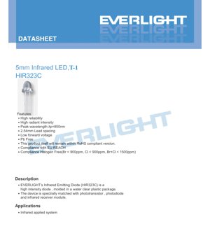
1. পণ্যের সারসংক্ষেপ
HIR323C হল একটি উচ্চ-তীব্রতার ইনফ্রারেড ইমিটার ডায়োড, যা স্ট্যান্ডার্ড T-1 (5mm) প্যাকেজে নির্মিত এবং স্বচ্ছ প্লাস্টিক লেন্স দিয়ে সজ্জিত। এই ডিভাইসটি ইনফ্রারেড সেন্সিং এবং কমিউনিকেশন সিস্টেমে নির্ভরযোগ্য কর্মক্ষমতা প্রদানের জন্য বিশেষভাবে ডিজাইন করা হয়েছে। এর বর্ণালী আউটপুট সাধারণ সিলিকন ফটোট্রানজিস্টর, ফটোডায়োড এবং ইনফ্রারেড রিসিভার মডিউলের সাথে সামঞ্জস্যপূর্ণ করার জন্য বিশেষভাবে মিলানো হয়েছে, যা সিস্টেমের সর্বোচ্চ দক্ষতা নিশ্চিত করে। এই উপাদানটির প্রধান প্রয়োগ ক্ষেত্র হল ইনফ্রারেড অ্যাপ্লিকেশন সিস্টেম, যার মধ্যে রয়েছে রিমোট কন্ট্রোল, বস্তু সনাক্তকরণ, প্রক্সিমিটি সেন্সিং এবং ফটোইলেকট্রিক সুইচ।
1.1 মূল সুবিধা এবং লক্ষ্য বাজার
এই ইনফ্রারেড LED-এর মূল সুবিধা এর নকশা এবং উপাদান নির্বাচন থেকে উদ্ভূত। এটি GaAlAs (গ্যালিয়াম অ্যালুমিনিয়াম আর্সেনাইড) চিপ উপাদান ব্যবহার করে, যা দক্ষ ইনফ্রারেড নির্গমনের জন্য পরিচিত। এই প্যাকেজিং উচ্চ বিকিরণ তীব্রতা প্রদান করে, যা শক্তিশালী সংকেত প্রেরণ সক্ষম করে। একটি উল্লেখযোগ্য বৈশিষ্ট্য হল এর কম ফরওয়ার্ড ভোল্টেজ, যা চূড়ান্ত প্রয়োগে শক্তি খরচ কমাতে সাহায্য করে। পণ্যটি আধুনিক পরিবেশগত ও নিরাপত্তা মানদণ্ড মেনে নকশা করা হয়েছে, যা সীসামুক্ত, RoHS সম্মত, EU REACH নিয়ন্ত্রণ মেনে চলে এবং হ্যালোজেন মুক্ত। এটি এটিকে বিশ্বব্যাপী বাজারের জন্য উপযুক্ত করে তোলে, বিশেষ করে ভোক্তা ইলেকট্রনিক্স, শিল্প স্বয়ংক্রিয়করণ এবং নিরাপত্তা ব্যবস্থায় যেখানে নির্ভরযোগ্য, দীর্ঘায়ু ইনফ্রারেড উৎস প্রয়োজন।
2. প্রযুক্তিগত পরামিতির গভীর বিশ্লেষণ
এই বিভাগে স্পেসিফিকেশন শীটে উল্লিখিত মূল প্রযুক্তিগত প্যারামিটারগুলির বিশদ ও নিরপেক্ষ ব্যাখ্যা প্রদান করা হয়েছে, যা ডিজাইন ইঞ্জিনিয়ারদের জন্য তাদের তাৎপর্য বর্ণনা করে।
2.1 পরম সর্বোচ্চ রেটিং
এই রেটিংগুলি ডিভাইসের স্থায়ী ক্ষতির কারণ হতে পারে এমন চাপের সীমা নির্ধারণ করে। এই শর্তে অপারেশনের কোনো গ্যারান্টি দেওয়া হয় না।
- অবিচ্ছিন্ন ফরওয়ার্ড কারেন্ট (IF):100 mA। এটি নির্দিষ্ট শর্তে LED-এর মাধ্যমে অনির্দিষ্টকাল প্রবাহিত হতে পারে এমন সর্বোচ্চ DC কারেন্ট।
- পিক ফরওয়ার্ড কারেন্ট (IFP):1.0 A। এই উচ্চ কারেন্ট শুধুমাত্র পালস শর্তে অনুমোদিত (পালস প্রস্থ ≤ 100μs, ডিউটি সাইকেল ≤ 1%)। এটি অত্যন্ত সংক্ষিপ্ত, উচ্চ-তীব্রতার পালস প্রয়োজন এমন অ্যাপ্লিকেশনের জন্য প্রযোজ্য।
- রিভার্স ভোল্টেজ (VR):5 V। রিভার্স বায়াস দিকে এই ভোল্টেজের বেশি হলে জাংশন ব্রেকডাউন হতে পারে।
- কাজ ও সংরক্ষণ তাপমাত্রা:পরিসীমা -40°C থেকে +85°C (কাজ) এবং -40°C থেকে +100°C (সংরক্ষণ)। এই প্রশস্ত পরিসর কঠোর পরিবেশে নির্ভরযোগ্যতা নিশ্চিত করে।
- শক্তি খরচ (Pd):পরিবেষ্টিত তাপমাত্রা ২৫°C বা তার কম হলে এটি ১৫০ mW। এটি হল প্যাকেজ দ্বারা তাপ হিসাবে অপচয় করা যেতে পারে এমন সর্বোচ্চ শক্তি। উচ্চতর পরিবেষ্টিত তাপমাত্রায় প্রকৃত অনুমোদিত ফরওয়ার্ড কারেন্ট হ্রাস পায়।
2.2 অপটোইলেকট্রিক বৈশিষ্ট্য
এই পরামিতিগুলি আদর্শ পরীক্ষার শর্তে (Ta=25°C) পরিমাপ করা হয়, যা ডিভাইসের কর্মক্ষমতা সংজ্ঞায়িত করে।
- বিকিরণ তীব্রতা (Ie):এটি প্রতি একক কঠিন কোণে নির্গত আলোর ক্ষমতা, যা mW/sr এককে পরিমাপ করা হয়। IF=20mA-এ, সাধারণ মান হল 30 mW/sr। 100mA পালস অপারেশনে, এটি 130 mW/sr পর্যন্ত পৌঁছাতে পারে। উচ্চতর বিকিরণ তীব্রতার অর্থ দীর্ঘতর অপারেটিং দূরত্ব বা উন্নত সংকেত-থেকে-শব্দ অনুপাত।
- সর্বোচ্চ তরঙ্গদৈর্ঘ্য (λp):850 nm (সাধারণ মান)। এটি আলোর আউটপুট পাওয়ার সর্বোচ্চ তরঙ্গদৈর্ঘ্য। 850nm নিকট-ইনফ্রারেড বর্ণালীর অন্তর্গত, যা মানুষের চোখে দৃশ্যমান নয়, তবে সিলিকন-ভিত্তিক সেন্সর দ্বারা কার্যকরভাবে শনাক্ত করা যায়।
- বর্ণালী ব্যান্ডউইথ (Δλ):45 nm (সাধারণ মান)। এটি সর্বোচ্চ তরঙ্গদৈর্ঘ্যকে কেন্দ্র করে নির্গমন তরঙ্গদৈর্ঘ্যের পরিসীমা সংজ্ঞায়িত করে। সংকীর্ণ ব্যান্ডউইথ পরিবেশগত আলোর শব্দ দূর করতে সহায়ক।
- ফরওয়ার্ড ভোল্টেজ (VF):20mA-এ 1.45V (টিপিক্যাল), সর্বোচ্চ 1.65V। 100mA (পালস)-এ সর্বোচ্চ 2.40V। কম VF একটি গুরুত্বপূর্ণ দক্ষতা প্যারামিটার।
- ভিউয়িং অ্যাঙ্গেল (2θ1/2):15 ডিগ্রি (টিপিক্যাল)। এটি সেই সম্পূর্ণ কোণ যখন বিকিরণ তীব্রতা তার সর্বোচ্চ মান (অক্ষীয়) এর অর্ধেকে নেমে আসে। সংকীর্ণ ভিউয়িং অ্যাঙ্গেল আরও ফোকাসড আলোর রশ্মি তৈরি করে।
3. গ্রেডিং সিস্টেমের ব্যাখ্যা
HIR323C একটি গ্রেডিং সিস্টেম ব্যবহার করে, যা 20mA স্ট্যান্ডার্ড টেস্ট কারেন্টে ডিভাইসের পরিমাপকৃত বিকিরণ তীব্রতার উপর ভিত্তি করে শ্রেণীবিভাগ করে। এটি ডিজাইনারদের তাদের অ্যাপ্লিকেশনের জন্য নির্দিষ্ট ন্যূনতম আউটপুট প্রয়োজনীয়তা পূরণ করে এমন উপাদান নির্বাচন করতে সক্ষম করে।
- P গ্রেড:বিকিরণ তীব্রতার পরিসীমা ১৫.০ mW/sr (ন্যূনতম) থেকে ২৪.০ mW/sr (সর্বোচ্চ) পর্যন্ত।
- Q মোড:বিকিরণ তীব্রতার পরিসীমা ২১.০ mW/sr (ন্যূনতম) থেকে ৩৪.০ mW/sr (সর্বোচ্চ) পর্যন্ত।
- R ড্রাইভ:বিকিরণ তীব্রতার পরিসীমা 30.0 mW/sr (ন্যূনতম) থেকে 48.0 mW/sr (সর্বোচ্চ) পর্যন্ত।
উচ্চতর গিয়ার নির্বাচন (যেমন R ড্রাইভ) উচ্চতর ন্যূনতম আউটপুট নিশ্চিত করে, যা সিস্টেমের কর্মক্ষমতার সামঞ্জস্যতা বজায় রাখার জন্য অত্যন্ত গুরুত্বপূর্ণ, বিশেষ করে তাপমাত্রার পরিবর্তন এবং পণ্যের জীবনকালের সময়।
4. পারফরম্যান্স কার্ভ বিশ্লেষণ
ডেটাশিটে বিভিন্ন চার্ট এবং গ্রাফ রয়েছে যা বিভিন্ন অবস্থার অধীনে ডিভাইসের আচরণ প্রদর্শন করে। একটি শক্তিশালী সার্কিট ডিজাইনের জন্য এগুলি বোঝা অত্যন্ত গুরুত্বপূর্ণ।
4.1 ফরওয়ার্ড কারেন্ট এবং পরিবেষ্টিত তাপমাত্রার সম্পর্ক
This curve shows the derating of maximum allowable continuous forward current with increasing ambient temperature. As temperature rises, the heat dissipation capability of the package decreases, necessitating a reduction in current to remain within the safe operating area (SOA) defined by maximum power dissipation. Designers must use this chart to select appropriate current-limiting resistors or drivers for their intended operating environment.
4.2 বিকিরণ তীব্রতা এবং ফরওয়ার্ড কারেন্টের সম্পর্ক
এই চিত্রটি ড্রাইভিং কারেন্ট (IF) এবং আলোক আউটপুট (Ie) এর মধ্যে সম্পর্ক বর্ণনা করে। এটি সাধারণত অরৈখিক হয়। কারেন্ট বৃদ্ধির সাথে আউটপুট বৃদ্ধি পায়, কিন্তু অত্যন্ত উচ্চ কারেন্টে তাপীয় প্রভাব এবং দক্ষতা প্রভাবের কারণে এটি স্যাচুরেশন হতে পারে। এই বক্ররেখা কাঙ্ক্ষিত আউটপুট স্তরে পৌঁছানোর জন্য প্রয়োজনীয় ড্রাইভিং কারেন্ট নির্ধারণে সহায়তা করে।
4.3 বর্ণালী বণ্টন
এই চিত্রটি তরঙ্গদৈর্ঘ্যের একটি ফাংশন হিসাবে আপেক্ষিক বিকিরণ তীব্রতা দেখায়। এটি শীর্ষ তরঙ্গদৈর্ঘ্য (λp ~850nm) এবং বর্ণালী ব্যান্ডউইথ (Δλ) নিশ্চিত করে। রিসিভিং সেন্সর (ফটোট্রানজিস্টর/ফটোডায়োড) এর বর্ণালী সংবেদনশীলতা বক্ররেখার সাথে সামঞ্জস্য নিশ্চিত করার জন্য এই বক্ররেখার আকৃতি অত্যন্ত গুরুত্বপূর্ণ।
4.4 আপেক্ষিক বিকিরণ তীব্রতা এবং কৌণিক সরণের সম্পর্ক
এই পোলার প্লটটি LED-এর নির্গমন প্যাটার্ন চিত্রিত করে। তীব্রতা কেন্দ্রীয় অক্ষ (0°) বরাবর সর্বোচ্চ এবং কোণ বৃদ্ধির সাথে সাথে হ্রাস পায়। 15-ডিগ্রি দৃশ্যমান কোণকে সেই অবস্থান হিসাবে সংজ্ঞায়িত করা হয় যেখানে তীব্রতা তার সর্বোচ্চ মানের 50%-এ নেমে আসে। সিস্টেমে আলোক রশ্মির বিস্তার এবং সংযোজন সহনশীলতা নির্ধারণের জন্য অপটিক্যাল ডিজাইনে এই তথ্য অত্যন্ত গুরুত্বপূর্ণ।
5. যান্ত্রিক এবং প্যাকেজিং তথ্য
5.1 প্যাকেজ মাত্রা চিত্র
ডিভাইসটি স্ট্যান্ডার্ড T-1 (5mm) বৃত্তাকার LED প্যাকেজ আউটলাইন মেনে চলে। প্রধান মাত্রার মধ্যে রয়েছে মোট ব্যাস (সাধারণত 5.0mm), লেন্স উচ্চতা এবং পিন পিচ (2.54mm বা 0.1 ইঞ্চি, যা একটি স্ট্যান্ডার্ড PCB হোল পিচ)। অঙ্কনটি অ্যানোড এবং ক্যাথোড পিন নির্দিষ্ট করে, দীর্ঘতর পিনটি সাধারণত অ্যানোড হয়। সকল অনির্দিষ্ট টলারেন্স হল ±0.25mm। PCB প্যাড ডিজাইন এবং যান্ত্রিক ক্লিয়ারেন্স চেক করার জন্য প্রকৌশলীদের অবশ্যই এই অঙ্কনটি দেখতে হবে।
5.2 পোলারিটি সনাক্তকরণ
এই উপাদানটি স্ট্যান্ডার্ড LED পোলারিটি কনভেনশন ব্যবহার করে: দীর্ঘতর পিনটি অ্যানোড (+) এবং সংক্ষিপ্ত পিনটি ক্যাথোড (-)। ক্যাথোড পিনের কাছাকাছি প্যাকেজের প্রান্তে একটি সমতল থাকতে পারে। সঠিক পোলারিটি অপারেশনের জন্য অত্যন্ত গুরুত্বপূর্ণ; 5V-এর বেশি বিপরীত পক্ষপাত ডিভাইসটির ক্ষতি করতে পারে।
6. সোল্ডারিং ও অ্যাসেম্বলি নির্দেশিকা
সঠিক হ্যান্ডলিং ডিভাইসের নির্ভরযোগ্যতা এবং কর্মক্ষমতা বজায় রাখার জন্য অত্যন্ত গুরুত্বপূর্ণ।
6.1 পিন গঠন
- অভ্যন্তরীণ চিপ এবং বন্ডিং তারের উপর চাপ এড়াতে ইপোক্সি বল বাবলের নীচ থেকে কমপক্ষে 3 মিমি দূরে বাঁকানো আবশ্যক।
- গঠন সর্বদা সোল্ডারিং প্রক্রিয়ার আগে সম্পন্ন করা উচিত।
- মোল্ডিং প্রক্রিয়ায় প্যাকেজের উপর যান্ত্রিক চাপ ন্যূনতম রাখতে হবে, যাতে ফাটল বা অভ্যন্তরীণ ক্ষতি রোধ করা যায়।
- ইনস্টলেশন চাপ এড়াতে PCB গর্তের সারিবদ্ধতা অবশ্যই সুনির্দিষ্ট হতে হবে।
6.2 সংরক্ষণের শর্ত
সুপারিশকৃত সংরক্ষণ পরিবেশ হল 30°C বা তার নিচে, আপেক্ষিক আর্দ্রতা (RH) 70% বা তার নিচে। এই শর্তে মেয়াদ উত্তীর্ণের তারিখ প্রেরণের পর ৩ মাস। দীর্ঘ সময়ের জন্য সংরক্ষণের জন্য (সর্বোচ্চ এক বছর), যন্ত্রাংশটি আর্দ্রতা শোষণ রোধ করতে নাইট্রোজেন বায়ুমণ্ডল এবং ডেসিক্যান্ট সহ একটি সিল করা পাত্রে সংরক্ষণ করা উচিত, যা সোল্ডারযোগ্যতা এবং নির্ভরযোগ্যতাকে প্রভাবিত করতে পারে।
6.3 ওয়েল্ডিং প্যারামিটার
তাপীয় ক্ষতি রোধ করতে সোল্ডার জয়েন্ট এবং ইপোক্সি রেজিন বাল্বের মধ্যে কমপক্ষে ৩ মিমি ন্যূনতম দূরত্ব বজায় রাখতে হবে।
- হ্যান্ড সোল্ডারিং:সোল্ডারিং আয়রন টিপের সর্বোচ্চ তাপমাত্রা ৩০০°C (৩০W সোল্ডারিং আয়রনের জন্য), প্রতিটি পিনের জন্য সর্বোচ্চ ৩ সেকেন্ড সোল্ডারিং সময়।
- ওয়েভ সোল্ডারিং / ডিপ সোল্ডারিং:প্রিহিটিং সর্বোচ্চ তাপমাত্রা 100°C, সর্বোচ্চ সময় 60 সেকেন্ড। সোল্ডার বাথ সর্বোচ্চ তাপমাত্রা 260°C, নিমজ্জন সময় 5 সেকেন্ডের বেশি নয়।
ডাটাশীট একটি প্রস্তাবিত সোল্ডারিং প্রোফাইল প্রদান করে, যা তাপীয় শক প্রতিরোধের জন্য গরম করার হার, সর্বোচ্চ তাপমাত্রা এবং শীতল করার হার নিয়ন্ত্রণের গুরুত্বের উপর জোর দেয়। সোল্ডারিং (ডিপ বা হ্যান্ড সোল্ডারিং) একবারের বেশি করা উচিত নয়। সোল্ডারিংয়ের পরে, ডিভাইসটি ঘরের তাপমাত্রায় শীতল না হওয়া পর্যন্ত কম্পন থেকে দূরে রাখতে হবে।
6.4 পরিষ্কার
যদি পরিষ্কার করার প্রয়োজন হয়, শুধুমাত্র রুম তাপমাত্রায় আইসোপ্রোপাইল অ্যালকোহল ব্যবহার করা যেতে পারে, যার সময়কাল এক মিনিটের বেশি নয়। আল্ট্রাসনিক ক্লিনিং ব্যবহার করার জন্য দৃঢ়ভাবে সুপারিশ করা হয় না, কারণ উচ্চ-ফ্রিকোয়েন্সি কম্পন LED-এর অভ্যন্তরীণ কাঠামো ক্ষতি করতে পারে। যদি একেবারেই প্রয়োজন হয়, প্রক্রিয়াটি অবশ্যই পূর্বে সাবধানে যাচাই করতে হবে।
7. প্যাকেজিং এবং অর্ডার তথ্য
7.1 প্যাকেজিং স্পেসিফিকেশন
ESD ক্ষতি রোধ করতে ডিভাইসগুলি সাধারণত ইলেক্ট্রোস্ট্যাটিক ডিসচার্জ (ESD) প্রতিরোধী ব্যাগে প্যাকেজ করা হয়। সাধারণ প্যাকেজিং কনফিগারেশন হল: প্রতি ব্যাগে ২০০-৫০০ পিস, ৫ ব্যাগ একটি অভ্যন্তরীণ বাক্সে, এবং ১০টি অভ্যন্তরীণ বাক্স একটি প্রধান (বাহ্যিক) কার্টনে রাখা হয়।
7.2 লেবেল ফরম্যাট স্পেসিফিকেশন
প্যাকেজিং-এর লেবেলে ট্রেসেবিলিটি এবং সঠিক প্রয়োগের জন্য গুরুত্বপূর্ণ তথ্য অন্তর্ভুক্ত থাকে:
- P/N:পণ্য নম্বর (HIR323C)।
- CAT:আলোকিত তীব্রতা গ্রেড (অর্থাৎ গ্রেডিং কোড: P, Q অথবা R)।
- LOT No:উৎপাদন ট্রেসেবিলিটির জন্য ব্যাচ নম্বর।
- অন্যান্য কোডে গ্রাহকের পার্ট নম্বর (CPN), পরিমাণ (QTY) এবং তারিখ কোড অন্তর্ভুক্ত থাকতে পারে।
8. প্রয়োগের সুপারিশ
8.1 সাধারণ প্রয়োগের দৃশ্যাবলী
- ইনফ্রারেড রিমোট কন্ট্রোল:টেলিভিশন, সাউন্ড সিস্টেম এবং অন্যান্য ভোক্তা ইলেকট্রনিক্স পণ্যের জন্য ব্যবহৃত হয়।
- অবজেক্ট/প্রক্সিমিটি সেন্সিং:গৃহস্থালি যন্ত্রপাতি, ভেন্ডিং মেশিন এবং শিল্প সরঞ্জামে বস্তুর উপস্থিতি বা অনুপস্থিতি শনাক্ত করতে ব্যবহৃত হয়।
- ফটোইলেকট্রিক সুইচ এবং এনকোডার:যেখানে ইনফ্রারেড বিমের বাধাপ্রাপ্তি বা প্রতিফলন অবস্থান বা গতি নির্দেশ করে।
- নিরাপত্তা ব্যবস্থা:ইনফ্রারেড অনুপ্রবেশ সনাক্তকরণ বিমের অংশ হিসেবে।
- ডেটা ট্রান্সমিশন:স্বল্প দূরত্ব, সিমপ্লেক্স সিরিয়াল ডেটা লিঙ্কের জন্য (IrDA সামঞ্জস্যপূর্ণ সিস্টেমের জন্য নির্দিষ্ট ডিভাইস প্রয়োজন হতে পারে)।
8.2 নকশা সংক্রান্ত বিবেচ্য বিষয়
- কারেন্ট সীমাবদ্ধতা:LED একটি কারেন্ট চালিত ডিভাইস। সর্বদা একটি সিরিজ রেজিস্টর বা কনস্ট্যান্ট কারেন্ট ড্রাইভার ব্যবহার করে ফরওয়ার্ড কারেন্ট (IF) কাঙ্ক্ষিত মানে সেট করুন, পাওয়ার সাপ্লাই ভোল্টেজ (Vcc), LED ফরওয়ার্ড ভোল্টেজ (VF) এবং কাঙ্ক্ষিত কারেন্টের ভিত্তিতে গণনা করুন: R = (Vcc - VF) / IF।
- তাপ ব্যবস্থাপনা:উচ্চতর কারেন্ট বা উচ্চতর পরিবেশগত তাপমাত্রায় ক্রমাগত অপারেশনের জন্য, ডিরেটিং কার্ভ বিবেচনা করুন। LED পিন থেকে তাপ বের করে নেওয়ার জন্য পর্যাপ্ত PCB কপার এরিয়া বা অন্যান্য পদ্ধতি নিশ্চিত করুন।
- অপটিক্যাল অ্যালাইনমেন্ট:15 ডিগ্রির সংকীর্ণ ভিউ অ্যাঙ্গেল সর্বোত্তম সিগন্যাল শক্তি পাওয়ার জন্য ইমিটার এবং ডিটেক্টরের মধ্যে সতর্ক যান্ত্রিক অ্যালাইনমেন্ট প্রয়োজন।
- পরিবেশগত আলোর হস্তক্ষেপ প্রতিরোধ:পরিবেশগত আলোর পরিবর্তন (যেমন সূর্যালোক) সহ পরিবেশে পরিচালিত সিস্টেমের জন্য, নির্দিষ্ট কম্পাঙ্কে ইনফ্রারেড সংকেত মডুলেট করার এবং সেই কম্পাঙ্কে টিউন করা রিসিভার ব্যবহার করে পটভূমি শব্দ দমন করার কথা বিবেচনা করুন।
9. প্রযুক্তিগত তুলনা ও পার্থক্য
যদিও অনেক 5mm ইনফ্রারেড LED বিদ্যমান, HIR323C প্যারামিটারের সমন্বয়ের মাধ্যমে নিজেকে আলাদা করেছে। এর উচ্চ সাধারণ বিকিরণ তীব্রতা (30 mW/sr at 20mA) একই প্যাকেজ আকারের মধ্যে এটি উচ্চ-কার্যক্ষমতার স্তরে রাখে। অত্যন্ত কম সাধারণ ফরওয়ার্ড ভোল্টেজ (1.45V) শক্তি দক্ষতা বাড়ায়, যা ব্যাটারি চালিত অ্যাপ্লিকেশনের জন্য বিশেষভাবে মূল্যবান। সিলিকন ফটোডিটেক্টরের সাথে নির্দিষ্ট মিল এবং কঠোর পরিবেশগত মান (হ্যালোজেন-মুক্ত, REACH) মেনে চলা এটিকে নির্ভরযোগ্য, দীর্ঘমেয়াদী কর্মক্ষমতা প্রয়োজন এমন আধুনিক পরিবেশ-বান্ধব ডিজাইনের জন্য একটি উপযুক্ত পছন্দ করে তোলে।
10. সাধারণ প্রশ্নাবলী (প্রযুক্তিগত প্যারামিটার ভিত্তিক)
Q1: আমি কি সরাসরি একটি 3.3V বা 5V মাইক্রোকন্ট্রোলার পিন থেকে এই LED চালাতে পারি?
A: না। LED এর কারেন্ট সীমিত করতে হবে। MCU পিনের মতো একটি কম ইম্পিডেন্স ভোল্টেজ সোর্সের সাথে সরাসরি সংযোগ করলে অতিরিক্ত কারেন্ট প্রবাহিত হবে, যা LED এবং MCU আউটপুট উভয়ই ক্ষতিগ্রস্ত করতে পারে। সীমিত কারেন্ট রেজিস্টর বা ড্রাইভার সার্কিট ব্যবহার করতে ভুলবেন না।
Q2: P, Q এবং R গ্রেডের মধ্যে পার্থক্য কী?
A: এগুলি বিভিন্ন গ্যারান্টিযুক্ত সর্বনিম্ন বিকিরণ আউটপুট স্তর উপস্থাপন করে। R গ্রেডের সর্বোচ্চ সর্বনিম্ন আউটপুট (30 mW/sr) রয়েছে, তারপরে Q গ্রেড (21 mW/sr), এবং তারপর P গ্রেড (15 mW/sr)। আপনার অ্যাপ্লিকেশনে প্রয়োজনীয় সংকেত শক্তি এবং লিঙ্ক মার্জিনের ভিত্তিতে নির্বাচন করুন।
Q3: ডেটাশিট অনুযায়ী সর্বোচ্চ ফরওয়ার্ড কারেন্ট 1A। আমি কি এটি উচ্চ-শক্তি পালস অ্যাপ্লিকেশনের জন্য ব্যবহার করতে পারি?
A: হ্যাঁ, তবে শুধুমাত্র উল্লিখিত কঠোর শর্তে: পালস প্রস্থ অবশ্যই 100 মাইক্রোসেকেন্ড বা তার কম হতে হবে, এবং ডিউটি সাইকেল অবশ্যই 1% বা তার কম হতে হবে (উদাহরণস্বরূপ, প্রতি 10ms-এ একটি 100μs পালস)। এটি LED-কে অতিরিক্ত গরম না করেই উচ্চ তাত্ক্ষণিক শক্তি পরিচালনা করতে দেয়।
Q4: স্টোরেজ শর্ত এবং শেলফ লাইফ কেন গুরুত্বপূর্ণ?
A: প্লাস্টিক প্যাকেজড ইলেকট্রনিক উপাদানগুলি বায়ুমণ্ডল থেকে আর্দ্রতা শোষণ করে। উচ্চ-তাপমাত্রা সোল্ডারিং প্রক্রিয়ার সময়, এই আটকে থাকা আর্দ্রতা দ্রুত প্রসারিত হয়, অভ্যন্তরীণ ডিল্যামিনেশন বা "পপকর্ন" প্রভাব সৃষ্টি করে, যা প্যাকেজিং ফাটিয়ে দেয় এবং ডিভাইসের ক্ষতি করে। উচ্চ ফলন উৎপাদন অর্জনের জন্য স্টোরেজ নির্দেশিকা মেনে চলা এবং প্রয়োজনে উপাদানগুলি বেক করা অত্যন্ত গুরুত্বপূর্ণ।
11. বাস্তব নকশা ও ব্যবহারের উদাহরণ
কেস স্টাডি: একটি সাধারণ বস্তু সনাক্তকরণ সেন্সর ডিজাইন করা।
একটি সাধারণ ব্যবহার হল বিম ইন্টারাপ্ট সেন্সর। HIR323C পথের একপাশে স্থাপন করা হয়, এবং একটি 850nm-এর সাথে মিলে যাওয়া ফটোট্রানজিস্টর সরাসরি বিপরীত দিকে স্থাপন করা হয়। একটি মাইক্রোকন্ট্রোলার একটি 100Ω রেজিস্টরের মাধ্যমে 5V পাওয়ার সাপ্লাই থেকে LED চালায়, ফলে ফরওয়ার্ড কারেন্ট প্রায় (5V - 1.45V)/100Ω = 35.5mA হয়। LED কে 1kHz ফ্রিকোয়েন্সি এবং 50% ডিউটি সাইকেলে পালস করে চালানো হয়, শক্তি সাশ্রয়ের জন্য এবং মাইক্রোকন্ট্রোলারে সিঙ্ক্রোনাস ডিটেকশনের মাধ্যমে পরিবেষ্টিত আলো দমন করার অনুমতি দেওয়ার জন্য। ফটোট্রানজিস্টরের আউটপুট MCU-এর ADC দ্বারা পড়া হয়। যখন কোনো বস্তু বিমকে বাধা দেয়, ADC রিডিং কমে যায়, যা একটি অ্যাকশন ট্রিগার করে। HIR323C-এর 15 ডিগ্রি সংকীর্ণ ভিউইং অ্যাঙ্গেল একটি সুনির্দিষ্ট সেন্সিং জোন তৈরি করতে সাহায্য করে, যার ফলে কাছাকাছি দিয়ে যাওয়া কিন্তু বিম অতিক্রম না করা বস্তুর কারণে মিথ্যা ট্রিগার কমে যায়।
12. নীতির পরিচিতি
ইনফ্রারেড লাইট এমিটিং ডায়োড (IR LED) হল একটি সেমিকন্ডাক্টর p-n জংশন ডায়োড যা ফরওয়ার্ড বায়াসে আলো নির্গত করে। যখন কারেন্ট অ্যানোড (p-টাইপ ম্যাটেরিয়াল) থেকে ক্যাথোড (n-টাইপ ম্যাটেরিয়াল) এর দিকে প্রবাহিত হয়, তখন জংশনে ইলেকট্রনগুলি হোলের সাথে পুনর্মিলিত হয় এবং ফোটন আকারে শক্তি মুক্ত করে। নির্গত আলোর তরঙ্গদৈর্ঘ্য সেমিকন্ডাক্টর উপাদানের ব্যান্ডগ্যাপ দ্বারা নির্ধারিত হয়। HIR323C-এর জন্য, GaAlAs উপাদান সিস্টেমের ব্যান্ডগ্যাপ 850 ন্যানোমিটার কাছাকাছি নিকট-ইনফ্রারেড অঞ্চলের ফোটনের সাথে সঙ্গতিপূর্ণ। স্বচ্ছ এপোক্সি লেন্স এই তরঙ্গদৈর্ঘ্যের জন্য স্বচ্ছ এবং প্রয়োজনীয় বিকিরণ প্যাটার্ন (ভিউইং অ্যাঙ্গেল) তৈরি করার জন্য গঠন করা হয়।
13. উন্নয়নের প্রবণতা
ইনফ্রারেড ইমিটার প্রযুক্তির উন্নয়নের প্রবণতা উচ্চতর দক্ষতার দিকে অব্যাহত রয়েছে (প্রতি ওয়াট বৈদ্যুতিক ইনপুট পাওয়ারের জন্য আরও আলোর আউটপুট পাওয়ার উৎপাদন), যা দীর্ঘতর দূরত্ব, কম শক্তি খরচ বা উভয়ই অর্জন করতে সক্ষম করে। ক্ষুদ্রীকরণও একটি প্রবণতা, যেখানে সারফেস মাউন্ট ডিভাইস (এসএমডি) প্যাকেজিং টি-১ এর মতো থ্রু-হোল টাইপের তুলনায় বেশি প্রচলিত, স্বয়ংক্রিয় সমাবেশের জন্য উপযুক্ত। একীকরণ আরেকটি প্রবণতা, যেখানে সম্মিলিত ইমিটার-সেন্সর মডিউল এবং অন্তর্নির্মিত সিগন্যাল প্রসেসিং সহ স্মার্ট সেন্সর সাধারণ হয়ে উঠছে। এছাড়াও, পরিবেশগত নিয়মকানুন (যেমন হ্যালোজেন-মুক্ত প্রয়োজনীয়তা) মেনে চলা এবং সেগুলো অতিক্রম করা বিশ্বব্যাপী বাজারকে সেবা প্রদানকারী উপাদান প্রস্তুতকারকদের জন্য একটি গুরুত্বপূর্ণ ফোকাস হিসেবে রয়ে গেছে। যদিও স্ট্যান্ডার্ড ৮৫০এনএম ভাল সিলিকন সেন্সর প্রতিক্রিয়া এবং কম খরচের কারণে এখনও জনপ্রিয়, তবে ৯৪০এনএম এর মতো অন্যান্য তরঙ্গদৈর্ঘ্য এমন অ্যাপ্লিকেশনের জন্য মনোযোগ পাচ্ছে যেখানে মৃদু লাল আলো (কিছু ৮৫০এনএম এলইডিতে উপস্থিত) দেখা যাওয়া অগ্রহণযোগ্য।
LED স্পেসিফিকেশন পরিভাষার বিস্তারিত ব্যাখ্যা
LED প্রযুক্তিগত পরিভাষার সম্পূর্ণ ব্যাখ্যা
১. অপটোইলেকট্রিক পারফরম্যান্সের মূল সূচক
| পরিভাষা | একক/প্রতীক | সাধারণ ব্যাখ্যা | কেন গুরুত্বপূর্ণ |
|---|---|---|---|
| Luminous Efficacy | lm/W (lumens per watt) | প্রতি ওয়াট বিদ্যুৎ থেকে নির্গত আলোক প্রবাহ, যত বেশি হবে তত বেশি শক্তি সাশ্রয়ী। | সরাসরি আলোর যন্ত্রের শক্তি দক্ষতার স্তর এবং বিদ্যুৎ বিলের খরচ নির্ধারণ করে। |
| আলোক প্রবাহ (Luminous Flux) | lm (লুমেন) | আলোর উৎস থেকে নির্গত মোট আলোর পরিমাণ, যা সাধারণভাবে "উজ্জ্বলতা" নামে পরিচিত। | এটি নির্ধারণ করে যে আলোক যন্ত্রটি যথেষ্ট উজ্জ্বল কিনা। |
| Viewing Angle | ° (ডিগ্রি), যেমন 120° | যে কোণে আলোর তীব্রতা অর্ধেক হয়ে যায়, যা আলোক রশ্মির প্রস্থ নির্ধারণ করে। | আলোকিত পরিসর ও সমতা প্রভাবিত করে। |
| বর্ণ তাপমাত্রা (CCT) | K (কেলভিন), যেমন 2700K/6500K | আলোর রঙের উষ্ণতা ও শীতলতা, কম মান হলুদ/উষ্ণ, বেশি মান সাদা/শীতল। | আলোর পরিবেশ এবং প্রযোজ্য দৃশ্যাবলী নির্ধারণ করে। |
| রঙ রেন্ডারিং ইনডেক্স (CRI / Ra) | এককহীন, ০–১০০ | আলোর উৎস দ্বারা বস্তুর প্রকৃত রঙ ফিরিয়ে আনার ক্ষমতা, Ra≥৮০ উত্তম। | রঙের সত্যতা প্রভাবিত করে, শপিং মল, আর্ট গ্যালারি ইত্যাদি উচ্চ চাহিদাসম্পন্ন স্থানে ব্যবহৃত হয়। |
| Color Fidelity (SDCM) | ম্যাকঅ্যাডাম উপবৃত্তের ধাপ সংখ্যা, যেমন "5-ধাপ" | রঙের সামঞ্জস্যের পরিমাণগত সূচক, ধাপ সংখ্যা যত কম, রঙের সামঞ্জস্য তত বেশি। | একই ব্যাচের আলোর যন্ত্রগুলির মধ্যে রঙের কোনো পার্থক্য নেই তা নিশ্চিত করা। |
| প্রাধান্যকারী তরঙ্গদৈর্ঘ্য (Dominant Wavelength) | nm (ন্যানোমিটার), যেমন 620nm (লাল) | রঙিন LED রঙের সাথে সম্পর্কিত তরঙ্গদৈর্ঘ্যের মান। | লাল, হলুদ, সবুজ ইত্যাদি একরঙা LED-এর রঙের আভা নির্ধারণ করে। |
| Spectral Distribution | তরঙ্গদৈর্ঘ্য বনাম তীব্রতা বক্ররেখা | LED থেকে নির্গত আলোর বিভিন্ন তরঙ্গদৈর্ঘ্যে তীব্রতা বণ্টন প্রদর্শন করে। | রঙের রেন্ডারিং এবং রঙের গুণমানকে প্রভাবিত করে। |
২. বৈদ্যুতিক প্যারামিটার
| পরিভাষা | প্রতীক | সাধারণ ব্যাখ্যা | নকশা বিবেচ্য বিষয় |
|---|---|---|---|
| Forward Voltage (Forward Voltage) | Vf | এলইডি জ্বলতে প্রয়োজনীয় সর্বনিম্ন ভোল্টেজ, একপ্রকার "চালু হওয়ার সীমা"। | ড্রাইভিং পাওয়ার সাপ্লাই ভোল্টেজ অবশ্যই ≥ Vf হতে হবে, একাধিক এলইডি সিরিজে সংযুক্ত হলে ভোল্টেজ যোগ হয়। |
| ফরওয়ার্ড কারেন্ট (Forward Current) | If | LED কে স্বাভাবিকভাবে আলোকিত করার জন্য প্রয়োজনীয় কারেন্টের মান। | সাধারণত ধ্রুব কারেন্ট ড্রাইভ ব্যবহার করা হয়, কারেন্ট উজ্জ্বলতা ও আয়ু নির্ধারণ করে। |
| সর্বোচ্চ পালস কারেন্ট (Pulse Current) | Ifp | স্বল্প সময়ের জন্য সহনীয় সর্বোচ্চ কারেন্ট, ডিমিং বা ফ্ল্যাশিংয়ের জন্য ব্যবহৃত। | পালস প্রস্থ এবং ডিউটি সাইকেল কঠোরভাবে নিয়ন্ত্রণ করতে হবে, অন্যথায় অতিরিক্ত গরম হয়ে ক্ষতি হতে পারে। |
| বিপরীত ভোল্টেজ (Reverse Voltage) | Vr | LED-এর সর্বোচ্চ বিপরীত ভোল্টেজ যা এটি সহ্য করতে পারে, অতিক্রম করলে এটি ভেঙে যেতে পারে। | সার্কিটে বিপরীত সংযোগ বা ভোল্টেজের আঘাত প্রতিরোধ করা প্রয়োজন। |
| তাপীয় রোধ (Thermal Resistance) | Rth (°C/W) | চিপ থেকে সোল্ডার পয়েন্টে তাপ স্থানান্তরের প্রতিরোধ, মান যত কম হবে, তাপ অপসারণ তত ভালো হবে। | উচ্চ তাপীয় প্রতিরোধের জন্য শক্তিশালী তাপ অপসারণ নকশা প্রয়োজন, অন্যথায় জংশন তাপমাত্রা বৃদ্ধি পায়। |
| ইলেক্ট্রোস্ট্যাটিক ডিসচার্জ ইমিউনিটি (ESD Immunity) | V (HBM), যেমন 1000V | ইলেক্ট্রোস্ট্যাটিক ডিসচার্জ প্রতিরোধ ক্ষমতা, মান যত বেশি হবে, ইলেক্ট্রোস্ট্যাটিক ড্যামেজ থেকে তত বেশি সুরক্ষিত। | উৎপাদন প্রক্রিয়ায় ইলেক্ট্রোস্ট্যাটিক সুরক্ষা ব্যবস্থা গ্রহণ করতে হবে, বিশেষ করে উচ্চ সংবেদনশীল LED-এর ক্ষেত্রে। |
তিন: তাপ ব্যবস্থাপনা ও নির্ভরযোগ্যতা
| পরিভাষা | মূল সূচক | সাধারণ ব্যাখ্যা | প্রভাব |
|---|---|---|---|
| Junction Temperature | Tj (°C) | LED চিপের অভ্যন্তরীণ প্রকৃত অপারেটিং তাপমাত্রা। | প্রতি 10°C হ্রাসে, আয়ু দ্বিগুণ হতে পারে; অত্যধিক তাপমাত্রা আলোক ক্ষয় এবং বর্ণ পরিবর্তনের কারণ হয়। |
| লুমেন ডিপ্রিসিয়েশন (Lumen Depreciation) | L70 / L80 (ঘন্টা) | প্রাথমিক মানের 70% বা 80% এ উজ্জ্বলতা হ্রাস পেতে প্রয়োজনীয় সময়। | LED-এর "সেবা জীবন" সরাসরি সংজ্ঞায়িত করা। |
| লুমেন রক্ষণাবেক্ষণ হার (Lumen Maintenance) | % (যেমন 70%) | একটি নির্দিষ্ট সময় ব্যবহারের পর অবশিষ্ট উজ্জ্বলতার শতাংশ। | দীর্ঘমেয়াদী ব্যবহারের পর উজ্জ্বলতা ধরে রাখার ক্ষমতা বোঝায়। |
| রঙের সরণ (Color Shift) | Δu′v′ বা ম্যাকঅ্যাডাম উপবৃত্ত | ব্যবহারের সময় রঙের পরিবর্তনের মাত্রা। | আলোক দৃশ্যের রঙের সামঞ্জস্যকে প্রভাবিত করে। |
| Thermal Aging | উপাদানের কর্মক্ষমতা হ্রাস | দীর্ঘমেয়াদী উচ্চ তাপমাত্রার কারণে এনক্যাপসুলেশন উপাদানের অবনতি। | উজ্জ্বলতা হ্রাস, রঙের পরিবর্তন বা ওপেন সার্কিট ব্যর্থতার কারণ হতে পারে। |
চার. এনক্যাপসুলেশন এবং উপকরণ
| পরিভাষা | সাধারণ প্রকার | সাধারণ ব্যাখ্যা | বৈশিষ্ট্য ও প্রয়োগ |
|---|---|---|---|
| প্যাকেজিং প্রকার | EMC, PPA, Ceramic | চিপ সুরক্ষা এবং অপটিক্যাল, থার্মাল ইন্টারফেস প্রদানকারী আবরণ উপাদান। | EMC-এর তাপ সহনশীলতা ভালো এবং খরচ কম; সিরামিকের তাপ অপসারণ উৎকৃষ্ট এবং আয়ু দীর্ঘ। |
| চিপ কাঠামো | ফরওয়ার্ড-মাউন্ট, ফ্লিপ চিপ (Flip Chip) | চিপ ইলেক্ট্রোড বিন্যাস পদ্ধতি। | ফ্লিপ-চিপ উত্তাপ অপসারণ ভাল, আলোর দক্ষতা বেশি, উচ্চ শক্তির জন্য উপযুক্ত। |
| ফসফর আবরণ | YAG, সিলিকেট, নাইট্রাইড | নীল আলোর চিপের উপর প্রলেপ দেওয়া হয়, আংশিকভাবে হলুদ/লাল আলোতে রূপান্তরিত হয় এবং সাদা আলোতে মিশ্রিত হয়। | বিভিন্ন ফসফর আলোর দক্ষতা, রঙের তাপমাত্রা এবং রঙ রেন্ডারিংকে প্রভাবিত করে। |
| লেন্স/অপটিক্যাল ডিজাইন | সমতল, মাইক্রোলেন্স, টোটাল ইন্টার্নাল রিফ্লেকশন | প্যাকেজিং পৃষ্ঠের অপটিক্যাল কাঠামো, আলোর বণ্টন নিয়ন্ত্রণ করে। | আলোক নির্গমন কোণ এবং আলোক বন্টন বক্ররেখা নির্ধারণ করে। |
পাঁচ. গুণমান নিয়ন্ত্রণ ও শ্রেণীবিভাগ
| পরিভাষা | শ্রেণীবিভাগের বিষয়বস্তু | সাধারণ ব্যাখ্যা | উদ্দেশ্য |
|---|---|---|---|
| আলোক প্রবাহ গ্রেডিং | কোড যেমন 2G, 2H | উজ্জ্বলতার স্তর অনুযায়ী গ্রুপ করুন, প্রতিটি গ্রুপের জন্য সর্বনিম্ন/সর্বোচ্চ লুমেন মান থাকবে। | একই ব্যাচের পণ্যগুলির উজ্জ্বলতা সামঞ্জস্যপূর্ণ তা নিশ্চিত করুন। |
| ভোল্টেজ গ্রেডিং | কোড যেমন 6W, 6X | ফরওয়ার্ড ভোল্টেজ রেঞ্জ অনুযায়ী গ্রুপিং। | ড্রাইভিং পাওয়ার ম্যাচিংয়ের সুবিধার্থে, সিস্টেমের দক্ষতা বৃদ্ধি। |
| রঙের পার্থক্য গ্রেডিং | 5-step MacAdam ellipse | রঙের স্থানাঙ্ক অনুযায়ী গ্রুপিং করুন, নিশ্চিত করুন যে রঙগুলি অত্যন্ত সীমিত পরিসরে পড়ে। | রঙের সামঞ্জস্য নিশ্চিত করুন, একই আলোর ফিক্সচারের মধ্যে রঙের অসামঞ্জস্যতা এড়িয়ে চলুন। |
| রঙের তাপমাত্রা শ্রেণীবিভাগ | 2700K, 3000K ইত্যাদি | রঙের তাপমাত্রা অনুযায়ী দলে বিভক্ত, প্রতিটি দলের জন্য নির্দিষ্ট স্থানাঙ্ক পরিসীমা রয়েছে। | বিভিন্ন দৃশ্যের রঙের তাপমাত্রার চাহিদা পূরণ করে। |
ছয়, পরীক্ষা ও প্রত্যয়ন
| পরিভাষা | মান/পরীক্ষা | সাধারণ ব্যাখ্যা | তাৎপর্য |
|---|---|---|---|
| LM-80 | লুমেন রক্ষণাবেক্ষণ পরীক্ষা | ধ্রুব তাপমাত্রার শর্তে দীর্ঘমেয়াদী আলোকসজ্জার মাধ্যমে উজ্জ্বলতা হ্রাসের তথ্য রেকর্ড করা হয়। | LED এর জীবনকাল গণনার জন্য (TM-21 এর সাথে সংমিশ্রণে)। |
| TM-21 | জীবনকাল প্রক্ষেপণ মান | LM-80 ডেটার উপর ভিত্তি করে ব্যবহারিক অবস্থায় জীবনকাল অনুমান। | বৈজ্ঞানিক জীবনকাল পূর্বাভাস প্রদান। |
| IESNA Standard | Illuminating Engineering Society Standard | অপটিক্যাল, বৈদ্যুতিক, এবং তাপীয় পরীক্ষার পদ্ধতি অন্তর্ভুক্ত করে। | শিল্পে স্বীকৃত পরীক্ষার ভিত্তি। |
| RoHS / REACH | পরিবেশগত প্রত্যয়ন | পণ্যটি ক্ষতিকারক পদার্থ (যেমন সীসা, পারদ) মুক্ত তা নিশ্চিত করা। | আন্তর্জাতিক বাজারে প্রবেশের শর্তাবলী। |
| ENERGY STAR / DLC | শক্তি দক্ষতা প্রত্যয়ন | আলোকসজ্জা পণ্যের জন্য শক্তি দক্ষতা ও কর্মক্ষমতা প্রত্যয়ন। | সাধারণত সরকারি ক্রয়, ভর্তুকি প্রকল্পে ব্যবহৃত হয়, বাজার প্রতিযোগিতা বৃদ্ধির জন্য। |