Table of Contents
- 1. পণ্য সংক্ষিপ্ত বিবরণ
- 2. প্রযুক্তিগত বিবরণের গভীর অনুসন্ধান
- 2.1 পরম সর্বোচ্চ রেটিং
- 2.2 ইলেক্ট্রো-অপটিক্যাল বৈশিষ্ট্য (Ta=25°C)
- 3. Binning System ব্যাখ্যা
- 4. Performance Curve Analysis
- 4.1 Forward Current vs. Forward Voltage (I-V Curve)
- 4.2 Luminous Intensity vs. Forward Current
- 4.3 Luminous Intensity vs. Ambient Temperature
- 4.4 Forward Current Derating Curve
- 4.5 Spectral Distribution
- 4.6 Radiation Diagram (Viewing Angle Pattern)
- 5. Mechanical & Package Information
- 5.1 প্যাকেজের মাত্রা
- 5.2 পোলারিটি শনাক্তকরণ
- 6. Soldering & Assembly Guidelines
- 6.1 আর্দ্রতা সংবেদনশীলতা ও সংরক্ষণ
- 6.2 রিফ্লো সোল্ডারিং প্রোফাইল (Pb-free)
- 6.3 হ্যান্ড সোল্ডারিং সতর্কতা
- 6.4 পুনর্বিন্যাস এবং মেরামত
- 7. Packaging & Ordering Information
- 7.1 টেপ এবং রিল স্পেসিফিকেশন
- 7.2 লেবেল এবং আর্দ্রতা প্রতিরোধী ব্যাগ
- 8. অ্যাপ্লিকেশন সুপারিশ
- 8.1 সাধারণ অ্যাপ্লিকেশন দৃশ্যকল্প
- 8.2 সমালোচনামূলক ডিজাইন বিবেচ্য বিষয়
- 9. Technical Comparison & Differentiation
- 10. প্রায়শই জিজ্ঞাসিত প্রশ্নাবলী (FAQs)
- 10.1 5V সরবরাহের সাথে সবুজ LED-এর জন্য আমার কোন রোধের মান ব্যবহার করা উচিত?
- 10.2 আমি কি একটি ধ্রুব ভোল্টেজ উৎস ব্যবহার করে কারেন্ট-সীমিত রোধ ছাড়াই এই LED চালাতে পারি?
- 10.3 নীল (BH) LED-এর জন্য সর্বোচ্চ ফরওয়ার্ড কারেন্ট কেন আলাদা?
- 10.4 আমি কীভাবে ±11% এর আলোকিত তীব্রতা সহনশীলতা ব্যাখ্যা করব?
- 10.5 এই LEDটি গাড়ির অভ্যন্তরীণ আলোর জন্য উপযুক্ত কি?
- 11. নকশা ও ব্যবহার কেস স্টাডি
- 12. কার্যনীতি
- 13. প্রযুক্তি প্রবণতা
- LED স্পেসিফিকেশন পরিভাষা
- Photoelectric Performance
- Electrical Parameters
- Thermal Management & Reliability
- Packaging & Materials
- Quality Control & Binning
- Testing & Certification
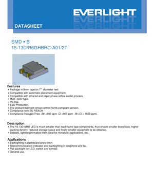
1. পণ্য সংক্ষিপ্ত বিবরণ
15-13D হল একটি কমপ্যাক্ট, সারফেস-মাউন্ট ডিভাইস (এসএমডি) এলইডি যা আধুনিক ইলেকট্রনিক প্রয়োগের জন্য নকশা করা হয়েছে, যেখানে ক্ষুদ্রায়ন এবং উচ্চ নির্ভরযোগ্যতা প্রয়োজন। এই সিরিজটি বিভিন্ন সেমিকন্ডাক্টর উপাদানের উপর ভিত্তি করে তিনটি স্বতন্ত্র রঙের বিকল্প প্রদান করে: ব্রিলিয়েন্ট রেড (আর৬, AlGaInP), ব্রিলিয়েন্ট গ্রিন (জিএইচ, InGaN), এবং ব্লু (বিএইচ, InGaN)। প্যাকেজটি ৭ ইঞ্চি ব্যাসের রিলে জড়ানো ৮মিমি টেপে সরবরাহ করা হয়, যা এটিকে উচ্চ-গতির স্বয়ংক্রিয় পিক-এন্ড-প্লেস সমাবেশ সরঞ্জামের সাথে সম্পূর্ণ সামঞ্জস্যপূর্ণ করে তোলে।
এই LED-এর প্রাথমিক সুবিধা হল ঐতিহ্যবাহী লিড-ফ্রেম প্যাকেজের তুলনায় এর উল্লেখযোগ্যভাবে হ্রাসকৃত ফুটপ্রিন্ট। এটি ডিজাইনারদের প্রিন্টেড সার্কিট বোর্ডে (PCBs) উচ্চতর উপাদান প্যাকিং ঘনত্ব অর্জন করতে সক্ষম করে, যার ফলে সামগ্রিক বোর্ডের আকার ছোট হয় এবং পরিণামে আরও কমপ্যাক্ট চূড়ান্ত পণ্য তৈরি হয়। এর হালকা গঠন এটিকে পোর্টেবল এবং ক্ষুদ্রাকৃতির অ্যাপ্লিকেশনের জন্য আদর্শ করে তোলে যেখানে ওজন এবং স্থান গুরুত্বপূর্ণ সীমাবদ্ধতা।
The product is manufactured to be Pb-free (lead-free), compliant with the EU RoHS and REACH directives, and meets halogen-free requirements (Bromine <900 ppm, Chlorine <900 ppm, Br+Cl < 1500 ppm). It is also produced using ESD (Electrostatic Discharge) safe processes, enhancing its handling reliability.
2. প্রযুক্তিগত বিবরণের গভীর অনুসন্ধান
2.1 পরম সর্বোচ্চ রেটিং
এই রেটিংগুলি সেই সীমা নির্ধারণ করে যার বাইরে ডিভাইসে স্থায়ী ক্ষতি হতে পারে। এই শর্তে অপারেশন নিশ্চিত করা হয় না।
- বিপরীত ভোল্টেজ (VR): সকল রঙের কোডের জন্য সর্বোচ্চ 5V। এটি অতিক্রম করলে জাংশন ব্রেকডাউন হতে পারে।
- ফরওয়ার্ড কারেন্ট (IF): R6 (লাল) এবং GH (সবুজ) এর জন্য 25 mA; BH (নীল) এর জন্য 20 mA। এটি সর্বোচ্চ অবিচ্ছিন্ন DC কারেন্ট।
- পিক ফরওয়ার্ড কারেন্ট (IFP): Applicable under pulsed conditions (1/10 duty cycle @ 1kHz). R6: 60 mA; GH & BH: 100 mA.
- পাওয়ার ডিসিপেশন (Pd): প্যাকেজটি সর্বোচ্চ যে পরিমাণ শক্তি অপচয় করতে পারে। R6: 60 mW; GH: 95 mW; BH: 75 mW। এটি IF * VF হিসাবে গণনা করা হয়।
- ইলেক্ট্রোস্ট্যাটিক ডিসচার্জ (ESD) HBM: সমস্ত ভেরিয়েন্ট ২০০০ভি হিউম্যান বডি মডেলের জন্য রেটেড, যা স্ট্যান্ডার্ড হ্যান্ডলিংয়ের জন্য ভাল অন্তর্নিহিত ইএসডি রোবাস্টনেস নির্দেশ করে।
- Operating & Storage Temperature: অপারেশনের জন্য -৪০°সি থেকে +৮৫°সি; স্টোরেজের জন্য -৪০°সি থেকে +৯০°সি।
- সোল্ডারিং তাপমাত্রা: রিফ্লো সোল্ডারিং শীর্ষ তাপমাত্রা: সর্বোচ্চ ১০ সেকেন্ডের জন্য ২৬০°সি। হ্যান্ড সোল্ডারিং: প্রতি টার্মিনালে সর্বোচ্চ ৩ সেকেন্ডের জন্য ৩৫০°সি।
2.2 ইলেক্ট্রো-অপটিক্যাল বৈশিষ্ট্য (Ta=25°C)
এগুলি স্ট্যান্ডার্ড টেস্ট শর্তে (IF=20mA, যদি অন্যথায় উল্লেখ না করা হয়) পরিমাপ করা সাধারণ পারফরম্যান্স প্যারামিটার।
- লুমিনাস ইনটেনসিটি (Iv): মিলিক্যান্ডেলায় (mcd) আলোর আউটপুট। R6: 90-140 mcd; GH: 112-180 mcd; BH: 45-70 mcd। ±11% সহনশীলতা প্রযোজ্য।
- Viewing Angle (2θ1/2): প্রায় 120 ডিগ্রি, নির্গত আলোর একটি প্রশস্ত কোণ প্রদান করে।
- Peak Wavelength (λp): যে তরঙ্গদৈর্ঘ্যে নির্গমন তীব্রতা সর্বোচ্চ। R6: 632 nm (Red); GH: 518 nm (Green); BH: 468 nm (Blue)।
- Dominant Wavelength (λd): মানব চোখ দ্বারা অনুভূত একক তরঙ্গদৈর্ঘ্য। R6: 624 nm; GH: 525 nm; BH: 470 nm।
- Spectral Bandwidth (Δλ): সর্বোচ্চ তীব্রতার অর্ধেক বিন্দুতে নির্গমন বর্ণালীর প্রস্থ। R6: 20 nm; GH: 35 nm; BH: 25 nm.
- Forward Voltage (VF): The voltage drop across the LED at the test current. R6: 1.70-2.40V (Typ. 2.00V); GH & BH: 2.70-3.70V (Typ. 3.30V). Tolerance is ±0.05V.
- Reverse Current (IR): Leakage current at VR=5V. R6: Max 10 μA; GH & BH: Not Applicable (NA).
3. Binning System ব্যাখ্যা
ডেটাশিটে উল্লেখ করা হয়েছে যে পণ্যটি মূল পরামিতির ভিত্তিতে LED-গুলিকে শ্রেণীবদ্ধ করতে একটি বিনিং সিস্টেম ব্যবহার করে, যার ফলে একটি ব্যাচের মধ্যে সামঞ্জস্য নিশ্চিত হয়। প্যাকেজিং-এর লেবেল ব্যাখ্যায় নির্দিষ্ট র্যাঙ্কের উল্লেখ রয়েছে:
- CAT (Luminous Intensity Rank): পরিমাপকৃত দীপ্তিমান তীব্রতা আউটপুট অনুসারে LED গুলিকে গ্রুপ করা হয়।
- HUE (Chromaticity Coordinates & Dominant Wavelength Rank): একটি অ্যারেতে রঙের তারতম্য কমাতে LED গুলিকে তাদের কালার পয়েন্ট বা প্রভাবশালী তরঙ্গদৈর্ঘ্য অনুসারে বাছাই করা হয়।
- REF (Forward Voltage Rank): LED গুলিকে তাদের ফরওয়ার্ড ভোল্টেজ ড্রপ অনুসারে শ্রেণীবদ্ধ করা হয়, যা সিরিজ বা প্যারালেল সার্কিটে কারেন্ট ম্যাচিংয়ের জন্য গুরুত্বপূর্ণ।
অ্যাপ্লিকেশনের জন্য রঙ বা তীব্রতা ম্যাচিং গুরুত্বপূর্ণ হলে, ডিজাইনারদের বিস্তারিত নির্বাচনের জন্য প্রস্তুতকারকের নির্দিষ্ট বিনিং চার্ট পরামর্শ করা উচিত।
4. Performance Curve Analysis
ডেটাশিট প্রতিটি LED টাইপের (R6, GH, BH) জন্য সাধারণ বৈশিষ্ট্য বক্ররেখা প্রদান করে। অ-মানক অবস্থার অধীনে ডিভাইসের আচরণ বোঝার জন্য এই গ্রাফগুলি অপরিহার্য।
4.1 Forward Current vs. Forward Voltage (I-V Curve)
এই বক্ররেখাটি কারেন্ট এবং ভোল্টেজের মধ্যে সূচকীয় সম্পর্ক দেখায়। "হাঁটু" ভোল্টেজ হল সেই বিন্দু যেখানে LED উল্লেখযোগ্যভাবে আলো নির্গত করা শুরু করে। প্রদত্ত সাধারণ VF মানগুলি 20mA এ পরিমাপ করা হয়। ডিজাইনাররা উপযুক্ত কারেন্ট-সীমাবদ্ধ রোধক নির্বাচন করতে এই বক্ররেখা ব্যবহার করেন।
4.2 Luminous Intensity vs. Forward Current
এই গ্রাফটি প্রদর্শন করে যে আলোর আউটপুট সাধারণত ফরোয়ার্ড কারেন্টের সমানুপাতিক, কিন্তু খুব উচ্চ কারেন্টে তাপীয় এবং দক্ষতা প্রভাবের কারণে এটি উপ-রৈখিক হয়ে উঠতে পারে। কাঙ্ক্ষিত উজ্জ্বলতা অর্জনের জন্য প্রয়োজনীয় ড্রাইভ কারেন্ট নির্ধারণের জন্য এটি অত্যন্ত গুরুত্বপূর্ণ।
4.3 Luminous Intensity vs. Ambient Temperature
জাংশন তাপমাত্রা বৃদ্ধির সাথে সাথে LED-এর আলোর আউটপুট হ্রাস পায়। উচ্চ তাপমাত্রার পরিবেশে পরিচালিত অ্যাপ্লিকেশনের জন্য এই ডিরেটিং কার্ভ অত্যন্ত গুরুত্বপূর্ণ। এটি পরিবেষ্টন তাপমাত্রা বৃদ্ধির সাথে সাথে অবশিষ্ট আপেক্ষিক দীপ্তিমান তীব্রতার শতাংশ দেখায়।
4.4 Forward Current Derating Curve
অতিরিক্ত গরম হওয়া রোধ করতে, পরিবেষ্টন তাপমাত্রা বৃদ্ধির সাথে সাথে সর্বোচ্চ অনুমোদিত অবিচ্ছিন্ন ফরোয়ার্ড কারেন্ট হ্রাস করতে হবে। এই কার্ভটি ডিভাইসের তাপমাত্রা পরিসীমা জুড়ে নিরাপদ অপারেটিং এরিয়া (SOA) প্রদান করে।
4.5 Spectral Distribution
এই প্লটটি তরঙ্গদৈর্ঘ্য বর্ণালী জুড়ে নির্গত আলোর আপেক্ষিক তীব্রতা দেখায়। এটি সর্বোচ্চ এবং প্রভাবশালী তরঙ্গদৈর্ঘ্য নিশ্চিত করে এবং নির্গত রঙের বর্ণালী বিশুদ্ধতা (সংকীর্ণতা) চিত্রিত করে।
4.6 Radiation Diagram (Viewing Angle Pattern)
আলোর তীব্রতার স্থানিক বণ্টন চিত্রিত করে একটি পোলার প্লট। 15-13D-এর একটি সাধারণ ল্যাম্বার্টিয়ান বা ওয়াইড-এঙ্গেল প্যাটার্ন রয়েছে, কেন্দ্রীয় অক্ষ থেকে কোণ বৃদ্ধির সাথে সাথে তীব্রতা হ্রাস পায়, আনুমানিক ±60 ডিগ্রি (মোট 120-ডিগ্রি দেখার কোণ) এ অর্ধেক তীব্রতায় পৌঁছায়।
5. Mechanical & Package Information
5.1 প্যাকেজের মাত্রা
15-13D প্যাকেজের নামমাত্র মাত্রা হল 1.5mm (দৈর্ঘ্য) x 1.3mm (প্রস্থ) x 0.8mm (উচ্চতা)। বিশেষভাবে উল্লেখ না করা হলে সহনশীলতা সাধারণত ±0.1mm হয়। উপাদানটির প্যাকেজের শীর্ষে পোলারিটি শনাক্তকরণের জন্য একটি অ্যানোড চিহ্ন (সাধারণত একটি খাঁজ, সবুজ বিন্দু বা অন্য কোনও নির্দেশক) রয়েছে। একটি প্রস্তাবিত PCB ল্যান্ড প্যাটার্ন (প্যাড লেআউট) প্রদান করা হয়েছে, তবে ডিজাইনারদের তাদের নির্দিষ্ট PCB উৎপাদন প্রক্রিয়া এবং তাপীয়/যান্ত্রিক প্রয়োজনীয়তার ভিত্তিতে এটি পরিবর্তন করার পরামর্শ দেওয়া হচ্ছে।
5.2 পোলারিটি শনাক্তকরণ
LED-এর সঠিক অপারেশনের জন্য সঠিক পোলারিটি অপরিহার্য। প্যাকেজে অ্যানোড (+) টার্মিনাল নির্দেশ করে একটি চাক্ষুষ চিহ্নিতকারী অন্তর্ভুক্ত রয়েছে। PCB ডিজাইন এবং সংযোজনকালে, সঠিক অভিমুখ নিশ্চিত করতে এই চিহ্নিতকারীকে বোর্ড লেআউটের সংশ্লিষ্ট অ্যানোড প্যাডের সাথে সারিবদ্ধ করতে হবে।
6. Soldering & Assembly Guidelines
6.1 আর্দ্রতা সংবেদনশীলতা ও সংরক্ষণ
LED গুলিকে আর্দ্রতা শোষণ রোধ করতে ডেসিক্যান্ট সহ একটি আর্দ্রতা-প্রতিরোধী ব্যারিয়ার ব্যাগে প্যাকেজ করা হয়েছে, যা রিফ্লো সোল্ডারিংয়ের সময় "পপকর্নিং" (প্যাকেজ ক্র্যাকিং) ঘটাতে পারে।
- ব্যবহারের জন্য প্রস্তুত না হওয়া পর্যন্ত ব্যাগটি খুলবেন না।
- খোলার পর, অব্যবহৃত অংশগুলি ≤30°C এবং ≤60% RH তে সংরক্ষণ করা উচিত।
- ব্যাগ খোলার পর "ফ্লোর লাইফ" হল 168 ঘন্টা (7 দিন)।
- সীমা অতিক্রম করলে, বা ডেসিক্যান্ট ইন্ডিকেটরের রং পরিবর্তিত হলে, সোল্ডারিংয়ের আগে ৬০±৫°সে তাপমাত্রায় ২৪ ঘন্টা বেক-আউট প্রয়োজন।
6.2 রিফ্লো সোল্ডারিং প্রোফাইল (Pb-free)
লেড-ফ্রি সোল্ডারের (যেমন: SAC305) জন্য একটি সুপারিশকৃত তাপমাত্রা প্রোফাইল প্রদান করা হয়েছে:
- প্রি-হিটিং: ১৫০-২০০°সে তাপমাত্রায় ৬০-১২০ সেকেন্ড।
- Time Above Liquidus (TAL): >217°C for 60-150 seconds.
- Peak Temperature: 260°C maximum, held for no more than 10 seconds.
- Ramp-up Rate: Maximum 3°C/sec to 255°C, then max 6°C/sec to peak.
- Ramp-down Rate: Controlled to avoid thermal shock.
Critical Note: একই LED অ্যাসেম্বলিতে দুইবারের বেশি রিফ্লো সোল্ডারিং করা উচিত নয়।
6.3 হ্যান্ড সোল্ডারিং সতর্কতা
যদি ম্যানুয়াল সোল্ডারিং প্রয়োজন হয়, অত্যন্ত সতর্কতা অবলম্বন করতে হবে:
- Use a soldering iron with a tip temperature <350°C.
- প্রতি টার্মিনালে যোগাযোগের সময় ≤3 সেকেন্ডে সীমাবদ্ধ রাখুন।
- ≤25W পাওয়ার রেটিং সহ একটি আয়রন ব্যবহার করুন।
- তাপ জমে যাওয়া রোধ করতে প্রতিটি টার্মিনাল সোল্ডারিংয়ের মধ্যে কমপক্ষে 2 সেকেন্ডের ব্যবধান দিন।
- সোল্ডার করার সময় LED বডিতে যান্ত্রিক চাপ প্রয়োগ করা এড়িয়ে চলুন।
6.4 পুনর্বিন্যাস এবং মেরামত
প্রাথমিক সোল্ডারিংয়ের পরে মেরামত করা অত্যন্ত নিরুৎসাহিত। যদি অনিবার্য হয়, তবে LED ডাই এবং ওয়্যার বন্ডের উপর তাপীয় চাপ কমানোর জন্য উভয় টার্মিনাল একসাথে গরম করতে একটি বিশেষায়িত ডাবল-হেড সোল্ডারিং আয়রন ব্যবহার করা উচিত। LED-এর বৈশিষ্ট্যের ক্ষতির সম্ভাবনা আগে থেকেই মূল্যায়ন করতে হবে।
7. Packaging & Ordering Information
7.1 টেপ এবং রিল স্পেসিফিকেশন
কম্পোনেন্টগুলি 15-13D প্যাকেজের জন্য উপযুক্ত মাত্রাসহ উত্তল ক্যারিয়ার টেপে সরবরাহ করা হয়। টেপটি একটি স্ট্যান্ডার্ড ৭-ইঞ্চি (১৭৮মিমি) ব্যাসের রিলে পেঁচানো থাকে। প্রতিটি রিলে ২০০০টি পিস থাকে। বিস্তারিত রিল, ক্যারিয়ার টেপ এবং পকেটের মাত্রা ডেটাশিটে দেওয়া আছে, যার স্ট্যান্ডার্ড সহনশীলতা হল ±০.১মিমি।
7.2 লেবেল এবং আর্দ্রতা প্রতিরোধী ব্যাগ
বাইরের আর্দ্রতা-প্রতিরোধী ব্যাগে একটি লেবেল থাকে যাতে গুরুত্বপূর্ণ তথ্য থাকে: কাস্টমার পার্ট নম্বর (CPN), ম্যানুফ্যাকচারার পার্ট নম্বর (P/N), পরিমাণ (QTY), এবং লুমিনাস ইনটেনসিটি (CAT), ক্রোমাটিসিটি (HUE), এবং ফরওয়ার্ড ভোল্টেজ (REF)-এর জন্য বিনিং কোড। ট্রেসেবিলিটির জন্য একটি লট নম্বর (LOT No.) অন্তর্ভুক্ত থাকে।
8. অ্যাপ্লিকেশন সুপারিশ
8.1 সাধারণ অ্যাপ্লিকেশন দৃশ্যকল্প
- ব্যাকলাইটিং: ড্যাশবোর্ড সূচক, সুইচ আলোকসজ্জা, কিয়াপ্যাড ব্যাকলাইট।
- টেলিকমিউনিকেশন সরঞ্জাম: ফোন, ফ্যাক্স মেশিন, রাউটার এবং মডেমে অবস্থা নির্দেশক।
- এলসিডি ফ্ল্যাট ব্যাকলাইটিং: ছোট মনোক্রোম বা কালার এলসিডি ডিসপ্লের জন্য এজ-লাইটিং।
- সাধারণ নির্দেশক ব্যবহার: কনজিউমার ইলেকট্রনিক্স, গৃহস্থালি যন্ত্রপাতি এবং শিল্প নিয়ন্ত্রণে পাওয়ার অবস্থা, মোড ইঙ্গিত, সতর্কতা সংকেত।
8.2 সমালোচনামূলক ডিজাইন বিবেচ্য বিষয়
- কারেন্ট লিমিটিং: ফরওয়ার্ড কারেন্ট সীমিত করতে একটি বাহ্যিক সিরিজ রেজিস্টর বাধ্যতামূলক। LED-এর এক্সপোনেনশিয়াল I-V বৈশিষ্ট্যের অর্থ হল একটি ছোট ভোল্টেজ বৃদ্ধি একটি বড়, ধ্বংসাত্মক কারেন্ট সার্জ ঘটাতে পারে। রেজিস্টর মান হিসাব করা হয় R = (Vsupply - VF) / IF।
- থার্মাল ম্যানেজমেন্ট: প্যাকেজটি ছোট হলেও, পাওয়ার ডিসিপেশন (Pd) বিবেচনা করতে হবে, বিশেষ করে উচ্চ পরিবেষ্টিত তাপমাত্রা বা ড্রাইভ কারেন্টে। সর্বোচ্চ রেটিংয়ের কাছাকাছি কাজ করলে পর্যাপ্ত PCB কপার এরিয়া বা থার্মাল ভায়া নিশ্চিত করুন।
- ESD প্রোটেকশন: যদিও এটি 2000V HBM-এর জন্য রেটেড, সংবেদনশীল ইনপুট লাইনে ESD সুরক্ষা বাস্তবায়ন বা উৎপাদনে ESD-সেফ হ্যান্ডলিং পদ্ধতি ব্যবহার করাকে ভালো অনুশীলন বলে বিবেচনা করা হয়।
- ওয়েভ সোল্ডারিং: ডেটাশিট শুধুমাত্র রিফ্লো এবং হ্যান্ড সোল্ডারিং নির্দিষ্ট করে। অত্যধিক তাপীয় এক্সপোজারের কারণে এই ধরনের SMD LED-এর জন্য সাধারণত ওয়েভ সোল্ডারিং সুপারিশ করা হয় না।
- বোর্ড ফ্লেক্সিং: এলইডিগুলো সোল্ডার করার পর পিসিবি বাঁকানো বা ফ্লেক্স করা এড়িয়ে চলুন, কারণ এটি সোল্ডার জয়েন্ট এবং এলইডি প্যাকেজ নিজেই চাপের মধ্যে ফেলতে পারে।
9. Technical Comparison & Differentiation
15-13D সিরিজটি নিজেকে আলাদা করে তার খুব ছোট 1.5x1.3mm ফুটপ্রিন্ট এবং তার আকারের তুলনায় অপেক্ষাকৃত উচ্চ লুমিনাস ইনটেনসিটির সমন্বয়ের মাধ্যমে, বিশেষ করে সবুজ এবং লাল ভেরিয়েন্টে। 120-ডিগ্রির প্রশস্ত দৃশ্যমান কোণ বিস্তৃত দৃশ্যমানতা প্রয়োজন এমন অ্যাপ্লিকেশনের জন্য উপযুক্ত। স্ট্যান্ডার্ড এসএমডি অ্যাসেম্বলি এবং সীসামুক্ত রিফ্লো প্রক্রিয়ার সাথে এর সামঞ্জস্য এটিকে আধুনিক, পরিবেশ-সম্মত উৎপাদনের সাথে সঙ্গতিপূর্ণ করে। বড় এসএমডি এলইডিগুলোর (যেমন, 0603, 0805) তুলনায়, এটি স্থান সাশ্রয় করে কিন্তু আরও সুনির্দিষ্ট প্লেসমেন্ট সরঞ্জামের প্রয়োজন হতে পারে। চিপ-স্কেল প্যাকেজের তুলনায়, এটি একটি আরও শক্তিশালী, এনক্যাপসুলেটেড কাঠামো প্রদান করে যা সহজে হ্যান্ডেল এবং নির্ভরযোগ্যভাবে সোল্ডার করা যায়।
10. প্রায়শই জিজ্ঞাসিত প্রশ্নাবলী (FAQs)
10.1 5V সরবরাহের সাথে সবুজ LED-এর জন্য আমার কোন রোধের মান ব্যবহার করা উচিত?
সাধারণ মান ব্যবহার করে: Vsupply = 5V, VF (GH, typ) = 3.3V, IF = 20mA। R = (5V - 3.3V) / 0.020A = 85 Ohms। নিকটতম স্ট্যান্ডার্ড মান হবে 82 বা 91 Ohms। সব অবস্থার অধীনে কারেন্ট সীমার মধ্যে থাকে তা নিশ্চিত করতে সর্বদা ডেটাশিট থেকে সর্বনিম্ন/সর্বোচ্চ VF ব্যবহার করে পুনরায় গণনা করুন।
10.2 আমি কি একটি ধ্রুব ভোল্টেজ উৎস ব্যবহার করে কারেন্ট-সীমিত রোধ ছাড়াই এই LED চালাতে পারি?
না। এটি প্রায় নিশ্চিতভাবেই LED টি ধ্বংস করবে। LED গুলি কারেন্ট-চালিত ডিভাইস। একটি ধ্রুব ভোল্টেজ উৎস LED-এর অত্যন্ত অ-রৈখিক জাংশনের মধ্য দিয়ে প্রবাহিত কারেন্ট নিয়ন্ত্রণ করতে পারে না। একটি সিরিজ রেজিস্টর অথবা, আরও ভাল পারফরম্যান্সের জন্য, একটি ধ্রুব কারেন্ট ড্রাইভার সার্কিট প্রয়োজন।
10.3 নীল (BH) LED-এর জন্য সর্বোচ্চ ফরওয়ার্ড কারেন্ট কেন আলাদা?
কম সর্বোচ্চ অবিচ্ছিন্ন কারেন্ট (লাল/সবুজের জন্য 25mA বনাম নীলের জন্য 20mA) সম্ভবত অভ্যন্তরীণ সেমিকন্ডাক্টর কাঠামোর পার্থক্য (নীল/সবুজের জন্য InGaN বনাম লালের জন্য AlGaInP) এবং উচ্চতর কারেন্ট ঘনত্বে এর সংশ্লিষ্ট তাপীয় বৈশিষ্ট্য ও দক্ষতার কারণে, যা নীল প্রকারের জন্য একটি কম পাওয়ার ডিসিপেশন (Pd) রেটিং-এর দিকে নিয়ে যায়।
10.4 আমি কীভাবে ±11% এর আলোকিত তীব্রতা সহনশীলতা ব্যাখ্যা করব?
এর অর্থ হল একটি উৎপাদন ব্যাচ থেকে যেকোনো পৃথক LED-এর প্রকৃত পরিমাপকৃত লুমিনাস ইনটেনসিটি ডেটাশিটে উল্লিখিত সাধারণ বা নামমাত্র মান থেকে ±11% পর্যন্ত পরিবর্তিত হতে পারে। উদাহরণস্বরূপ, 180 mcd-এর একটি সাধারণ Iv সহ একটি সবুজ LED প্রায় 160 mcd থেকে 200 mcd পর্যন্ত যেকোনো জায়গায় পরিমাপ করতে পারে। অভিন্ন উজ্জ্বলতা প্রয়োজন এমন অ্যাপ্লিকেশনের জন্য, একটি টাইট বিন (CAT কোড) থেকে LED নির্বাচন করা প্রয়োজন।
10.5 এই LEDটি গাড়ির অভ্যন্তরীণ আলোর জন্য উপযুক্ত কি?
যদিও এটি কিছু অ-সমালোচনামূলক স্বয়ংচালিত অভ্যন্তরীণ অ্যাপ্লিকেশনে ব্যবহার করা যেতে পারে (যেমন সুইচ ব্যাকলাইটিং), ডেটাশিটে একটি নির্দিষ্ট অ্যাপ্লিকেশন সীমাবদ্ধতা নোট অন্তর্ভুক্ত রয়েছে যা "উচ্চ নির্ভরযোগ্যতার অ্যাপ্লিকেশন যেমন সামরিক/বিমানচালনা, স্বয়ংচালিত নিরাপত্তা/নিরাপত্তা ব্যবস্থা এবং চিকিৎসা সরঞ্জাম" এ ব্যবহারের বিরুদ্ধে পরামর্শ দেয়। যেকোনো স্বয়ংচালিত অ্যাপ্লিকেশনের জন্য, বিশেষত নিরাপত্তা-সম্পর্কিত, একটি উপাদান যা বিশেষভাবে স্বয়ংচালিত-গ্রেড মানদণ্ডে (যেমন, AEC-Q102) যোগ্যতা অর্জন করেছে তা অবশ্যই ব্যবহার করতে হবে।
11. নকশা ও ব্যবহার কেস স্টাডি
দৃশ্যকল্প: একটি ভোক্তা রাউটারের জন্য একটি মাল্টি-স্ট্যাটাস ইন্ডিকেটর প্যানেল ডিজাইন করা।
একজন ডিজাইনারকে পাওয়ার (সবুজ), ইন্টারনেট অ্যাক্টিভিটি (ফ্ল্যাশিং সবুজ) এবং ইথারনেট লিংক (অ্যাম্বার/লাল) নির্দেশ করতে হবে। স্থান সীমিত। তারা পাওয়ারের জন্য একটি 15-13D/GH (সবুজ), ইন্টারনেটের জন্য একটি (MCU দ্বারা ফ্ল্যাশ করা), এবং ইথারনেট ইন্ডিকেটরের জন্য একটি 15-13D/R6 (লাল) বেছে নেয় (অ্যাম্বার একটি লাল LED-কে কম কারেন্টে চালনা করে বা একটি ডিফিউজার ব্যবহার করে অনুমান করা যেতে পারে)।
বাস্তবায়ন: MCU GPIO পিনগুলি 3.3V। সবুজ LED-গুলির জন্য (VF টিপিক্যাল 3.3V), ভোল্টেজ ড্রপ সরবরাহ ভোল্টেজের প্রায় সমান, ফলে রোধকের জন্য খুব কম হেডরুম থাকে। ডিজাইনার পর্যাপ্ত উজ্জ্বলতা অর্জন এবং নির্ভরযোগ্যভাবে চালু নিশ্চিত করতে কম কারেন্ট (যেমন 10mA) ব্যবহার করতে পারেন, R = (3.3V - 3.3V)/0.01A = 0 Ohms হিসাব করে। এটি সমস্যাযুক্ত। পরিবর্তে, তারা একটি ট্রানজিস্টর বা একটি কারেন্ট-সিঙ্ক মোডে কনফিগার করা GPIO পিন ব্যবহার করবে যা LED-এর ক্যাথোডের সাথে সংযুক্ত থাকে, এবং অ্যানোড একটি উপযুক্ত রোধকের মাধ্যমে উচ্চতর ভোল্টেজ রেলের (যেমন 5V) সাথে যুক্ত থাকে। এই কেসটি LED-এর VF-এর সাথে ড্রাইভার সার্কিটের ভোল্টেজ মেলানোর গুরুত্ব তুলে ধরে।
12. কার্যনীতি
লাইট এমিটিং ডায়োড (LED) হল সেমিকন্ডাক্টর p-n জংশন ডিভাইস যা ইলেক্ট্রোলুমিনেসেন্স নামক প্রক্রিয়ার মাধ্যমে আলো নির্গত করে। যখন একটি ফরোয়ার্ড ভোল্টেজ প্রয়োগ করা হয়, তখন n-টাইপ অঞ্চল থেকে ইলেকট্রন এবং p-টাইপ অঞ্চল থেকে হোলগুলি জংশন জুড়ে ইনজেক্ট হয়। এই চার্জ বাহকগুলি জংশনের কাছাকাছি সক্রিয় অঞ্চলে পুনর্মিলিত হয়। দক্ষ LED-এর জন্য, এই পুনর্মিলন একটি ডাইরেক্ট ব্যান্ডগ্যাপ সেমিকন্ডাক্টর উপাদানে ঘটে। পুনর্মিলনের সময় মুক্ত শক্তি একটি ফোটন (আলোর কণা) হিসাবে নির্গত হয়। নির্গত আলোর তরঙ্গদৈর্ঘ্য (রঙ) সেমিকন্ডাক্টর উপাদানের ব্যান্ডগ্যাপ শক্তি (Eg) দ্বারা নির্ধারিত হয়: E = hc/λ, যেখানে h হল প্ল্যাঙ্কের ধ্রুবক, c হল আলোর গতি, এবং λ হল তরঙ্গদৈর্ঘ্য। 15-13D লাল আলোর জন্য AlGaInP (কম শক্তি/দীর্ঘ তরঙ্গদৈর্ঘ্যের জন্য বড় ব্যান্ডগ্যাপ) এবং সবুজ ও নীল আলোর জন্য InGaN (উচ্চ শক্তি/সংক্ষিপ্ত তরঙ্গদৈর্ঘ্যের জন্য ছোট ব্যান্ডগ্যাপ) ব্যবহার করে। এপোক্সি রজন লেন্স আলোর আউটপুট গঠন করে এবং পরিবেশগত সুরক্ষা প্রদান করে।
13. প্রযুক্তি প্রবণতা
15-13D একটি পরিপক্ক SMD LED প্রযুক্তির প্রতিনিধিত্ব করে। নির্দেশক LED বাজারের সাধারণ প্রবণতাগুলি অব্যাহতভাবে নিম্নলিখিত দিকে অগ্রসর হচ্ছে:
- আরও ক্ষুদ্রায়ন: আরও ছোট প্যাকেজ (যেমন, ১.০x০.৫মিমি, চিপ-স্কেল) আলোর নিঃসরণ বজায় রেখে বা উন্নত করে।
- উচ্চতর দক্ষতা: প্রতি ওয়াটে উন্নত লুমেন (লুমেন/ওয়াট) বা প্রতি মিলিঅ্যাম্পে মিলিক্যান্ডেলা (এমসিডি/এমএ), প্রদত্ত উজ্জ্বলতার জন্য শক্তি খরচ হ্রাস।
- উন্নত নির্ভরযোগ্যতা ও মজবুতি: উচ্চতর সর্বোচ্চ জাংশন তাপমাত্রা, উন্নত আর্দ্রতা প্রতিরোধ, এবং উচ্চ-তাপমাত্রা অপারেটিং লাইফ (এইচটিওএল) পরীক্ষায় উন্নত কর্মক্ষমতা।
- সমন্বিত সমাধান: এলইডি যাতে অন্তর্নির্মিত কারেন্ট-লিমিটিং রেজিস্টর, সুরক্ষা ডায়োড (ইএসডি, রিভার্স পোলারিটি), বা এমনকি একটি প্যাকেজে ড্রাইভার আইসি থাকে।
- বিস্তৃত রঙের ব্যাপ্তি ও সামঞ্জস্য: রঙ এবং তীব্রতার জন্য কঠোর বিনিং, সম্পূর্ণ-রঙের ডিসপ্লে এবং নির্দেশক অ্যারের চাহিদা মেটাতে যেখানে দৃশ্যমান অভিন্নতা অত্যন্ত গুরুত্বপূর্ণ।
যদিও নতুন প্যাকেজ বিদ্যমান, 15-13D সাধারণ-উদ্দেশ্য নির্দেশক অ্যাপ্লিকেশনের জন্য একটি নির্ভরযোগ্য এবং ব্যাপকভাবে ব্যবহৃত কার্যকরী উপাদান হিসাবে রয়ে গেছে, যেখানে এর আকার, কর্মক্ষমতা এবং খরচের ভারসাম্য সর্বোত্তম।
LED স্পেসিফিকেশন পরিভাষা
LED প্রযুক্তিগত পরিভাষার সম্পূর্ণ ব্যাখ্যা
Photoelectric Performance
| পরিভাষা | ইউনিট/প্রতিনিধিত্ব | সরল ব্যাখ্যা | কেন গুরুত্বপূর্ণ |
|---|---|---|---|
| Luminous Efficacy | lm/W (lumens per watt) | বিদ্যুতের প্রতি ওয়াটে আলোর আউটপুট, যত বেশি হবে শক্তি তত বেশি দক্ষ। | সরাসরি শক্তি দক্ষতা গ্রেড এবং বিদ্যুতের খরচ নির্ধারণ করে। |
| Luminous Flux | lm (lumens) | উৎস থেকে নির্গত মোট আলো, সাধারণত "উজ্জ্বলতা" নামে পরিচিত। | আলোটি যথেষ্ট উজ্জ্বল কিনা তা নির্ধারণ করে। |
| Viewing Angle | ° (ডিগ্রি), উদাহরণস্বরূপ, 120° | যে কোণে আলোর তীব্রতা অর্ধেক কমে যায়, এটি বিমের প্রস্থ নির্ধারণ করে। | আলোকিত পরিসর এবং সমরূপতা প্রভাবিত করে। |
| CCT (কালার টেম্পারেচার) | K (কেলভিন), উদাহরণস্বরূপ, 2700K/6500K | আলোর উষ্ণতা/শীতলতা, কম মান হলুদাভ/উষ্ণ, বেশি মান সাদাটে/শীতল। | আলোকসজ্জার পরিবেশ এবং উপযুক্ত দৃশ্যপট নির্ধারণ করে। |
| CRI / Ra | এককহীন, ০–১০০ | বস্তুর রং সঠিকভাবে উপস্থাপনের ক্ষমতা, Ra≥৮০ ভালো। | রঙের সত্যতা প্রভাবিত করে, শপিং মল, যাদুঘরের মতো উচ্চ চাহিদাসম্পন্ন স্থানে ব্যবহৃত হয়। |
| SDCM | MacAdam ellipse steps, e.g., "5-step" | Color consistency metric, smaller steps mean more consistent color. | Ensures uniform color across same batch of LEDs. |
| Dominant Wavelength | nm (nanometers), e.g., 620nm (red) | Wavelength corresponding to color of colored LEDs. | লাল, হলুদ, সবুজ একরঙা LED-এর বর্ণচ্ছটার মাত্রা নির্ধারণ করে। |
| Spectral Distribution | Wavelength vs intensity curve | তরঙ্গদৈর্ঘ্যের উপর তীব্রতার বণ্টন প্রদর্শন করে। | বর্ণ পুনরুৎপাদন এবং গুণমানকে প্রভাবিত করে। |
Electrical Parameters
| পরিভাষা | Symbol | সরল ব্যাখ্যা | Design Considerations |
|---|---|---|---|
| Forward Voltage | Vf | LED চালু করার জন্য সর্বনিম্ন ভোল্টেজ, যেমন "শুরুর থ্রেশহোল্ড"। | ড্রাইভার ভোল্টেজ অবশ্যই ≥Vf হতে হবে, সিরিজ LED-এর জন্য ভোল্টেজ যোগ হয়। |
| ফরওয়ার্ড কারেন্ট | If | সাধারণ LED অপারেশনের জন্য কারেন্ট মান। | Usually constant current drive, current determines brightness & lifespan. |
| সর্বোচ্চ পালস কারেন্ট | Ifp | সংক্ষিপ্ত সময়ের জন্য সহনীয় সর্বোচ্চ কারেন্ট, ডিমিং বা ফ্ল্যাশিংয়ের জন্য ব্যবহৃত। | Pulse width & duty cycle must be strictly controlled to avoid damage. |
| রিভার্স ভোল্টেজ | Vr | LED সহ্য করতে পারে এমন সর্বোচ্চ বিপরীত ভোল্টেজ, এর বেশি হলে ব্রেকডাউন হতে পারে। | সার্কিটকে বিপরীত সংযোগ বা ভোল্টেজ স্পাইক প্রতিরোধ করতে হবে। |
| তাপীয় প্রতিরোধ | Rth (°C/W) | চিপ থেকে সোল্ডারে তাপ স্থানান্তরের প্রতিরোধ, যত কম তত ভালো। | উচ্চ তাপীয় প্রতিরোধের জন্য শক্তিশালী তাপ অপসারণ প্রয়োজন। |
| ESD ইমিউনিটি | V (HBM), উদাহরণস্বরূপ, 1000V | স্থিরতা বিদ্যুৎ স্রাব সহ্য করার ক্ষমতা, উচ্চ মান কম ঝুঁকিপূর্ণ বোঝায়। | উৎপাদনে অ্যান্টি-স্ট্যাটিক ব্যবস্থা প্রয়োজন, বিশেষত সংবেদনশীল LED-এর জন্য। |
Thermal Management & Reliability
| পরিভাষা | মূল মেট্রিক | সরল ব্যাখ্যা | প্রভাব |
|---|---|---|---|
| জাংশন তাপমাত্রা | Tj (°C) | LED চিপের ভিতরের প্রকৃত অপারেটিং তাপমাত্রা। | প্রতি 10°C হ্রাস আয়ু দ্বিগুণ করতে পারে; অত্যধিক উচ্চ তাপমাত্রা আলোর ক্ষয় এবং রঙের পরিবর্তন ঘটায়। |
| Lumen Depreciation | L70 / L80 (hours) | প্রাথমিক উজ্জ্বলতার 70% বা 80% এ নেমে আসতে সময়। | সরাসরি LED "সার্ভিস লাইফ" সংজ্ঞায়িত করে। |
| লুমেন মেইনটেন্যান্স | % (উদাহরণস্বরূপ, 70%) | সময়ের পর বজায় রাখা উজ্জ্বলতার শতাংশ। | দীর্ঘমেয়াদী ব্যবহারে উজ্জ্বলতা ধরে রাখার ক্ষমতা নির্দেশ করে। |
| কালার শিফট | Δu′v′ বা ম্যাকঅ্যাডাম উপবৃত্ত | ব্যবহারের সময় রঙের পরিবর্তনের মাত্রা। | আলোক দৃশ্যে রঙের সামঞ্জস্যকে প্রভাবিত করে। |
| Thermal Aging | Material degradation | দীর্ঘমেয়াদী উচ্চ তাপমাত্রার কারণে অবনতি। | উজ্জ্বলতা হ্রাস, রঙের পরিবর্তন বা ওপেন-সার্কিট ব্যর্থতার কারণ হতে পারে। |
Packaging & Materials
| পরিভাষা | সাধারণ প্রকার | সরল ব্যাখ্যা | Features & Applications |
|---|---|---|---|
| প্যাকেজ প্রকার | EMC, PPA, Ceramic | হাউজিং উপাদান চিপ রক্ষা করে, অপটিক্যাল/থার্মাল ইন্টারফেস প্রদান করে। | EMC: ভাল তাপ প্রতিরোধ ক্ষমতা, কম খরচ; সিরামিক: ভাল তাপ অপসারণ, দীর্ঘ জীবনকাল। |
| চিপ স্ট্রাকচার | ফ্রন্ট, ফ্লিপ চিপ | চিপ ইলেক্ট্রোড বিন্যাস। | ফ্লিপ চিপ: ভাল তাপ অপসারণ, উচ্চ কার্যকারিতা, উচ্চ-শক্তির জন্য। |
| ফসফর আবরণ | YAG, সিলিকেট, নাইট্রাইড | নীল চিপ ঢেকে রাখে, কিছুকে হলুদ/লালে রূপান্তরিত করে, সাদা আলো তৈরি করতে মিশ্রিত করে। | বিভিন্ন ফসফর কার্যকারিতা, CCT, এবং CRI কে প্রভাবিত করে। |
| লেন্স/অপটিক্স | সমতল, মাইক্রোলেন্স, TIR | পৃষ্ঠের উপর অপটিক্যাল কাঠামো আলোর বণ্টন নিয়ন্ত্রণ করে। | দর্শন কোণ এবং আলোর বণ্টন বক্ররেখা নির্ধারণ করে। |
Quality Control & Binning
| পরিভাষা | Binning Content | সরল ব্যাখ্যা | উদ্দেশ্য |
|---|---|---|---|
| Luminous Flux Bin | কোড, উদাহরণস্বরূপ, 2G, 2H | উজ্জ্বলতা অনুসারে গোষ্ঠীবদ্ধ, প্রতিটি গোষ্ঠীর সর্বনিম্ন/সর্বোচ্চ লুমেন মান রয়েছে। | একই ব্যাচে অভিন্ন উজ্জ্বলতা নিশ্চিত করে। |
| Voltage Bin | কোড, উদাহরণস্বরূপ, 6W, 6X | ফরোয়ার্ড ভোল্টেজ পরিসীমা অনুসারে গোষ্ঠীবদ্ধ। | ড্রাইভার ম্যাচিং সহজতর করে, সিস্টেম দক্ষতা উন্নত করে। |
| কালার বিন | 5-step MacAdam ellipse | রঙের স্থানাঙ্ক অনুযায়ী গোষ্ঠীবদ্ধ, একটি সংকীর্ণ পরিসীমা নিশ্চিত করে। | রঙের সামঞ্জস্য নিশ্চিত করে, ফিক্সচারের মধ্যে অসম রঙ এড়ায়। |
| CCT Bin | 2700K, 3000K ইত্যাদি। | CCT অনুযায়ী শ্রেণীবদ্ধ, প্রতিটির নিজস্ব সংশ্লিষ্ট স্থানাঙ্ক পরিসীমা রয়েছে। | বিভিন্ন দৃশ্যের CCT প্রয়োজনীয়তা পূরণ করে। |
Testing & Certification
| পরিভাষা | Standard/Test | সরল ব্যাখ্যা | Significance |
|---|---|---|---|
| LM-80 | লুমেন রক্ষণাবেক্ষণ পরীক্ষা | ধ্রুব তাপমাত্রায় দীর্ঘমেয়াদী আলোকসজ্জা, উজ্জ্বলতা ক্ষয় রেকর্ড করা। | LED-এর আয়ু অনুমান করতে ব্যবহৃত (TM-21 সহ)। |
| TM-21 | জীবনকাল অনুমান মান | LM-80 ডেটার উপর ভিত্তি করে প্রকৃত অবস্থার অধীনে জীবনকাল অনুমান করে। | বৈজ্ঞানিক জীবনকাল পূর্বাভাস প্রদান করে। |
| IESNA | Illuminating Engineering Society | অপটিক্যাল, বৈদ্যুতিক, তাপীয় পরীক্ষা পদ্ধতি কভার করে। | শিল্প-স্বীকৃত পরীক্ষার ভিত্তি। |
| RoHS / REACH | পরিবেশগত প্রত্যয়ন | ক্ষতিকারক পদার্থ (সীসা, পারদ) নেই তা নিশ্চিত করে। | আন্তর্জাতিকভাবে বাজার প্রবেশের প্রয়োজনীয়তা। |
| ENERGY STAR / DLC | শক্তি দক্ষতা প্রত্যয়ন | আলোকসজ্জার জন্য শক্তি দক্ষতা এবং কর্মদক্ষতা প্রত্যয়ন। | সরকারি ক্রয়, ভর্তুকি কর্মসূচিতে ব্যবহৃত, প্রতিযোগিতামূলকতা বৃদ্ধি করে। |