কন্টেন্ট
- 1. পণ্য সংক্ষিপ্ত বিবরণ
- 2. গভীর প্রযুক্তিগত প্যারামিটার বিশ্লেষণ
- 2.1 পরম সর্বোচ্চ রেটিং
- 2.2 অপটোইলেকট্রিক বৈশিষ্ট্য
- 3. গ্রেডিং সিস্টেমের বিবরণ
- 3.1 আলোকিত তীব্রতা গ্রেডিং
- 3.2 প্রভাবশালী তরঙ্গদৈর্ঘ্য গ্রেডিং
- 3.3 ফরওয়ার্ড ভোল্টেজ গ্রেডিং
- 4. কর্মক্ষমতা বক্ররেখা বিশ্লেষণ
- 5. যান্ত্রিক ও প্যাকেজিং তথ্য
- 5.1 প্যাকেজ মাত্রা
- 5.2 স্বয়ংক্রিয় সমাবেশ প্যাকেজিং
- 6. সোল্ডারিং ও সমাবেশ নির্দেশিকা
- 6.1 স্টোরেজ ও আর্দ্রতা সংবেদনশীলতা
- 6.2 রিফ্লো সোল্ডারিং তাপমাত্রা প্রোফাইল
- 6.3 হ্যান্ড সোল্ডারিং ও রিপেয়ার
- 7. প্যাকেজিং ও অর্ডার তথ্য
- 8. প্রয়োগের পরামর্শ
- 8.1 সাধারণ প্রয়োগের দৃশ্যাবলী
- 8.2 মূল নকশা বিবেচনা
- 9. প্রযুক্তিগত তুলনা এবং পার্থক্য
- 10. সাধারণ প্রশ্নাবলী (FAQ)
- 10.1 সীমাবদ্ধ রোধ কেন একেবারেই প্রয়োজন?
- 10.2 আমি কি সরাসরি 3.3V বা 5V লজিক পাওয়ার দিয়ে এই LED চালাতে পারি?
- 10.3 বিন্যাস কোড (P1, CC4, 21) আমার ডিজাইনের জন্য কী অর্থ বহন করে?
- 10.4 ময়েশ্চার ব্যাগ খোলার পর ৭ দিনের ফ্লোর লাইফ কতটা গুরুত্বপূর্ণ?
- 11. বাস্তব ডিজাইন ও ব্যবহারের উদাহরণ
- 12. কার্যপ্রণালী
- 13. প্রযুক্তিগত প্রবণতা ও পটভূমি
- LED স্পেসিফিকেশন পরিভাষার বিস্তারিত ব্যাখ্যা
- ১. আলোক-বৈদ্যুতিক কর্মক্ষমতার মূল সূচক
- ২. বৈদ্যুতিক প্যারামিটার
- ৩. তাপ ব্যবস্থাপনা ও নির্ভরযোগ্যতা
- চার, প্যাকেজিং ও উপকরণ
- পাঁচ, গুণমান নিয়ন্ত্রণ ও গ্রেডিং
- ছয়, পরীক্ষণ ও প্রত্যয়ন
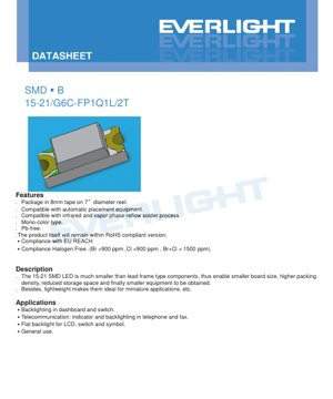
1. পণ্য সংক্ষিপ্ত বিবরণ
15-21/G6C-FP1Q1L/2T হল একটি সারফেস মাউন্ট ডিভাইস (এসএমডি) এলইডি যা আধুনিক কমপ্যাক্ট ইলেকট্রনিক অ্যাপ্লিকেশনের জন্য ডিজাইন করা হয়েছে। ঐতিহ্যবাহী লিড ফ্রেম এলইডির তুলনায়, এই উপাদানটি প্যাকেজিং আকার এবং ওজনে উল্লেখযোগ্য হ্রাস অর্জন করেছে, যা প্রযুক্তির একটি বড় অগ্রগতির প্রতিনিধিত্ব করে। এর প্রাথমিক কাজ হল একটি ক্ষুদ্র প্যাকেজের মধ্যে নির্ভরযোগ্য এবং দক্ষ আলোর উৎস প্রদান করা, যার ফলে প্রিন্টেড সার্কিট বোর্ডে (পিসিবি) উচ্চ উপাদান ঘনত্ব অর্জন করা যায় এবং ইলেকট্রনিক ডিভাইসের সামগ্রিক ক্ষুদ্রকরণে সহায়তা করে। মডেল নম্বরের "G6C" চিহ্নটি নির্দেশ করে যে এটি অভ্যন্তরীণভাবে AlGaInP (অ্যালুমিনিয়াম গ্যালিয়াম ইন্ডিয়াম ফসফাইড) সেমিকন্ডাক্টর উপাদান ব্যবহার করে এবং একটি জল-স্বচ্ছ রজন লেন্স দিয়ে সিল করা হয়েছে, একটি নির্দিষ্ট উজ্জ্বল হলুদ-সবুজ আলো নির্গত করতে সক্ষম।
এই এলইডির মূল সুবিধা এর এসএমডি কাঠামো থেকে উদ্ভূত। লিডহীন নকশা পরজীবী আবেশ হ্রাস করে এবং স্বয়ংক্রিয় পিক-অ্যান্ড-প্লেস সমাবেশকে সমর্থন করে, যার ফলে বৃহৎ আকারের উৎপাদন প্রক্রিয়া সহজ হয়। এর ছোট আকার (প্রায় 1.6mm x 0.8mm x 0.6mm) সরাসরি স্টোরেজ স্থানের প্রয়োজনীয়তা হ্রাস করে এবং চূড়ান্ত পণ্যগুলিকে আরও পাতলা করে ডিজাইন করা সম্ভব করে তোলে। উপরন্তু, পণ্যটি গুরুত্বপূর্ণ পরিবেশগত ও নিরাপত্তা প্রবিধান মেনে চলে, সীসামুক্ত, RoHS-সামঞ্জস্যপূর্ণ, REACH-সামঞ্জস্যপূর্ণ এবং হ্যালোজেন-মুক্ত বৈশিষ্ট্যযুক্ত, যা বৈশ্বিক ইলেকট্রনিক বাজারের কঠোর প্রয়োজনীয়তা পূরণ করে।
2. গভীর প্রযুক্তিগত প্যারামিটার বিশ্লেষণ
এলইডির কর্মক্ষমতা এবং সীমাবদ্ধতা তার বৈদ্যুতিক, অপটিক্যাল এবং তাপীয় স্পেসিফিকেশন দ্বারা সংজ্ঞায়িত করা হয়। নির্ভরযোগ্য সার্কিট ডিজাইন এবং দীর্ঘমেয়াদী কর্মক্ষমতা নিশ্চিত করার জন্য এই পরামিতিগুলির গভীর বোঝাপড়া অত্যন্ত গুরুত্বপূর্ণ।
2.1 পরম সর্বোচ্চ রেটিং
এই রেটিংগুলি সেই চাপের সীমা সংজ্ঞায়িত করে যা ডিভাইসের স্থায়ী ক্ষতি করতে পারে। এই সীমায় বা তার বাইরে অপারেশনের কোন গ্যারান্টি দেওয়া হয় না।
- বিপরীত ভোল্টেজ (VR):5V। বিপরীত বায়াসে এই ভোল্টেজ অতিক্রম করলে জাংশন ব্রেকডাউন হতে পারে।
- অবিচ্ছিন্ন ফরোয়ার্ড কারেন্ট (IF):25mA। এটি 25°C তাপমাত্রায় অবিচ্ছিন্ন অপারেশনের জন্য সর্বোচ্চ সুপারিশকৃত ডিসি কারেন্ট।
- পিক ফরোয়ার্ড কারেন্ট (IFP):60mA। এই কারেন্ট শুধুমাত্র পালস শর্তে অনুমোদিত (ডিউটি সাইকেল 1/10, ফ্রিকোয়েন্সি 1kHz), স্বল্প সময়ের জন্য উচ্চ উজ্জ্বলতা অর্জনে ব্যবহার করা যেতে পারে।
- পাওয়ার ডিসিপেশন (Pd):60mW। এটি হল প্যাকেজ দ্বারা তাপ হিসাবে অপসারিত হতে পারে এমন সর্বোচ্চ শক্তি, যা VF * IF সূত্র দ্বারা গণনা করা হয়।
- ইলেক্ট্রোস্ট্যাটিক ডিসচার্জ (ESD):2000V (হিউম্যান বডি মডেল)। এই রেটিং নির্দেশ করে যে ডিভাইসটির মাঝারি মাত্রার ESD সংবেদনশীলতা রয়েছে; সঠিক হ্যান্ডলিং পদ্ধতি অবশ্যই অনুসরণ করতে হবে।
- অপারেটিং এবং স্টোরেজ তাপমাত্রা:-40°C থেকে +85°C (অপারেটিং), -40°C থেকে +90°C (স্টোরেজ)। প্রশস্ত তাপমাত্রা পরিসর এটি বিভিন্ন পরিবেশগত অবস্থার জন্য উপযোগী করে তোলে।
- সোল্ডারিং তাপমাত্রা:260°C রিফ্লো সোল্ডারিং 10 সেকেন্ডের জন্য অথবা প্রতি পিনে 350°C হ্যান্ড সোল্ডারিং 3 সেকেন্ডের জন্য সহ্য করতে পারে।
2.2 অপটোইলেকট্রিক বৈশিষ্ট্য
এইগুলি 20mA ফরওয়ার্ড কারেন্ট (IF) এবং 25°C পরিবেষ্টিত তাপমাত্রায় (Ta) পরিমাপ করা সাধারণ পারফরম্যান্স প্যারামিটার।
- লুমিনাস ইনটেনসিটি (Iv):45.0 mcd (ন্যূনতম) থেকে 90.0 mcd (সর্বোচ্চ) পর্যন্ত পরিসীমা, সাধারণ সহনশীলতা ±11%। এটি উপলব্ধ উজ্জ্বলতা সংজ্ঞায়িত করে।
- ভিউইং অ্যাঙ্গেল (2θ1/2):130 ডিগ্রি (সাধারণ)। বিস্তৃত ভিউইং অ্যাঙ্গেল একটি প্রশত নির্গমন প্যাটার্ন প্রদান করে, যা এলাকা আলোকসজ্জা এবং সূচক অ্যাপ্লিকেশনের জন্য উপযুক্ত।
- পিক ওয়েভলেন্থ (λp):575 nm (সাধারণ)। এটি সেই তরঙ্গদৈর্ঘ্য যেখানে বর্ণালী শক্তি বন্টন সর্বোচ্চ মানে পৌঁছায়।
- ডমিনেন্ট ওয়েভলেন্থ (λd):570.0 nm থেকে 574.5 nm পর্যন্ত পরিসর। এটি মানুষের চোখ দ্বারা অনুভূত একরঙা তরঙ্গদৈর্ঘ্য, যা বর্ণের আভা (উজ্জ্বল হলুদ-সবুজ) সংজ্ঞায়িত করে। সহনশীলতা হল ±1nm।
- বর্ণালী ব্যান্ডউইথ (Δλ):20 nm (সাধারণ মান)। এটি সর্বোচ্চ তীব্রতার অর্ধেক বিন্দুতে নির্গমন বর্ণালীর প্রস্থ।
- ফরওয়ার্ড ভোল্টেজ (VF):20mA-তে, 1.70V থেকে 2.30V পর্যন্ত পরিসর, সাধারণ সহনশীলতা ±0.05V। এটি LED চালু হলে এর দুই প্রান্তে ভোল্টেজ ড্রপ।
- রিভার্স কারেন্ট (IR):VR=5V-তে, সর্বোচ্চ 10 μA। এই ডিভাইসটি বিপরীত দিকে কাজ করার জন্য নকশা করা হয়নি; এই প্যারামিটারটি শুধুমাত্র লিকেজ কারেন্ট পরীক্ষার জন্য।
3. গ্রেডিং সিস্টেমের বিবরণ
সেমিকন্ডাক্টর উৎপাদনের অন্তর্নিহিত পরিবর্তনশীলতার কারণে, LED গুলো তাদের কর্মক্ষমতার ভিত্তিতে গ্রেডে বিভক্ত করা হয়। এই সিস্টেম ডিজাইনারদের তাদের অ্যাপ্লিকেশনের জন্য সামঞ্জস্যের নির্দিষ্ট প্রয়োজনীয়তা অনুযায়ী উপাদান নির্বাচন করতে দেয়।
3.1 আলোকিত তীব্রতা গ্রেডিং
20mA তে পরিমাপ করা লিউমিনাস ইনটেনসিটির ভিত্তিতে, LED গুলো তিনটি গ্রেডে (P1, P2, Q1) বিভক্ত। উদাহরণস্বরূপ, Q1 গ্রেডে 72.0 থেকে 90.0 mcd এর মধ্যে ইনটেনসিটি সম্পন্ন LED গুলো থাকে। একটি একক গ্রেড নির্বাচন করা একটি অ্যারে মধ্যে একাধিক LED এর উজ্জ্বলতা সমান নিশ্চিত করে।
3.2 প্রভাবশালী তরঙ্গদৈর্ঘ্য গ্রেডিং
রঙের সামঞ্জস্য বজায় রাখার জন্য, LED গুলো তাদের ডমিনেন্ট ওয়েভলেংথ অনুযায়ী তিনটি গ্রুপে (CC2, CC3, CC4) বিভক্ত, যেখানে প্রতিটি গ্রুপ 570.0 nm থেকে 574.5 nm পর্যন্ত 1.5 nm পরিসর কভার করে। এই কঠোর নিয়ন্ত্রণ সেইসব অ্যাপ্লিকেশনের জন্য অত্যন্ত গুরুত্বপূর্ণ যেখানে রঙ ম্যাচিং অপরিহার্য।
3.3 ফরওয়ার্ড ভোল্টেজ গ্রেডিং
ফরওয়ার্ড ভোল্টেজ ছয়টি গ্রেডে (19 থেকে 24) বিভক্ত, যেখানে প্রতিটি গ্রেড 1.70V থেকে 2.30V পর্যন্ত 0.1V ধাপে বৃদ্ধি নির্দেশ করে। দক্ষ কারেন্ট-লিমিটিং সার্কিট ডিজাইন করতে, বিশেষ করে একাধিক সিরিজ-সংযুক্ত LED চালনা করার সময় সমান কারেন্ট বন্টন নিশ্চিত করতে, VF গ্রেড বোঝা অত্যন্ত গুরুত্বপূর্ণ।
4. কর্মক্ষমতা বক্ররেখা বিশ্লেষণ
যদিও ডেটাশিটে সাধারণ অপটোইলেকট্রিক বৈশিষ্ট্য কার্ভের উল্লেখ থাকে, তবে স্ট্যান্ডার্ড-বহির্ভূত অবস্থায় ডিভাইসের আচরণ বোঝার জন্য এই চার্টগুলি অত্যন্ত গুরুত্বপূর্ণ। ডিজাইনারদের সেমিকন্ডাক্টর পদার্থবিজ্ঞানের নীতির উপর ভিত্তি করে নিম্নলিখিত সম্পর্কগুলির পূর্বাভাস দেওয়া উচিত:
- IV কার্ভ (কারেন্ট বনাম ভোল্টেজ):থ্রেশহোল্ড ভোল্টেজ (প্রায় 1.7V) অতিক্রম করার পর, ফরওয়ার্ড কারেন্ট ফরওয়ার্ড ভোল্টেজের সাথে সূচকীয়ভাবে বৃদ্ধি পায়। এটি একটি কারেন্ট-সীমাবদ্ধ ডিভাইস (রেজিস্টর বা ড্রাইভার) ব্যবহারের চরম প্রয়োজনীয়তার উপর জোর দেয়।
- লুমিনাস ইনটেনসিটি বনাম কারেন্ট:তীব্রতা সাধারণত কারেন্ট বৃদ্ধির সাথে বৃদ্ধি পায়, কিন্তু অত্যন্ত উচ্চ কারেন্টে, তাপীয় প্রভাব এবং দক্ষতা হ্রাসের কারণে, এটি সম্পৃক্ত হতে পারে বা দক্ষতা কমে যেতে পারে।
- আলোক তীব্রতা বনাম তাপমাত্রা:আলোক আউটপুট সাধারণত জাংশন তাপমাত্রা বৃদ্ধির সাথে হ্রাস পায়। উচ্চ তাপমাত্রার পরিবেশ বা উচ্চ শক্তি প্রয়োগে এই তাপীয় ডিরেটিং বিবেচনা করা আবশ্যক।
- বর্ণালী সরণ বনাম তাপমাত্রা:প্রধান তরঙ্গদৈর্ঘ্য তাপমাত্রার সাথে সামান্য সরে যেতে পারে, যা সূক্ষ্ম প্রয়োগে রঙের উপলব্ধিকে প্রভাবিত করতে পারে।
5. যান্ত্রিক ও প্যাকেজিং তথ্য
5.1 প্যাকেজ মাত্রা
LED-এর একটি কমপ্যাক্ট আয়তাকার ফুটপ্রিন্ট রয়েছে। গুরুত্বপূর্ণ মাত্রা (একক: mm) অন্তর্ভুক্ত করে: বডির দৈর্ঘ্য 1.6, প্রস্থ 0.8, উচ্চতা 0.6। প্যাডগুলি নির্ভরযোগ্য সারফেস মাউন্টিংয়ের জন্য ডিজাইন করা হয়েছে। প্যাকেজে ক্যাথোড চিহ্ন স্পষ্টভাবে নির্দেশিত থাকে, যাতে সংযোজনকালে পোলারিটি সঠিক থাকে। সমস্ত অনুল্লিখিত সহনশীলতা হল ±0.1mm।
5.2 স্বয়ংক্রিয় সমাবেশ প্যাকেজিং
উপাদানগুলি পরিবেশগত আর্দ্রতা থেকে ক্ষতি রোধ করতে আর্দ্রতা-প্রতিরোধী প্যাকেজিং-এ সরবরাহ করা হয়। এগুলি ৮ মিমি প্রস্থের ক্যারিয়ার টেপে ৭ ইঞ্চি ব্যাসের রিলে পেঁচিয়ে সরবরাহ করা হয়, প্রতি রিলে ২০০০ টি। এই বিন্যাসটি স্ট্যান্ডার্ড অটোমেটেড প্লেসমেন্ট সরঞ্জামের সাথে সম্পূর্ণ সামঞ্জস্যপূর্ণ। রিল এবং ক্যারিয়ার টেপের মাত্রাগুলি ফিডার সিস্টেমের সাথে সামঞ্জস্য নিশ্চিত করার জন্য নির্দিষ্ট করা আছে।
6. সোল্ডারিং ও সমাবেশ নির্দেশিকা
ক্ষতি রোধ এবং নির্ভরযোগ্যতা নিশ্চিত করার জন্য সঠিক হ্যান্ডলিং অত্যন্ত গুরুত্বপূর্ণ।
6.1 স্টোরেজ ও আর্দ্রতা সংবেদনশীলতা
LED-এর আর্দ্রতা সংবেদনশীলতা (MSL) রয়েছে। ব্যবহারের আগে আর্দ্রতা-প্রতিরোধী ব্যাগ খোলা উচিত নয়। খোলার পরে, অব্যবহৃত উপাদানগুলিকে অবশ্যই ≤৩০°C এবং ≤৬০% RH অবস্থায় সংরক্ষণ করতে হবে এবং ১৬৮ ঘন্টার (৭ দিন) মধ্যে ব্যবহার করতে হবে। এই সময়সীমা অতিক্রান্ত হলে, ব্যবহারের আগে ৬০±৫°C তাপমাত্রায় ২৪ ঘন্টা বেক করতে হবে।
6.2 রিফ্লো সোল্ডারিং তাপমাত্রা প্রোফাইল
সীসামুক্ত রিফ্লো সোল্ডারিং তাপমাত্রা প্রোফাইল নির্দিষ্ট করা হয়েছে:
- প্রিহিটিং: 150-200°C, 60-120 সেকেন্ড স্থায়ী।
- তরল রেখার উপরে সময় (217°C): 60-150 সেকেন্ড।
- সর্বোচ্চ তাপমাত্রা: সর্বাধিক 260°C, 10 সেকেন্ডের বেশি নয়।
- তাপমাত্রা বৃদ্ধির হার: সর্বাধিক 6°C/সেকেন্ড।
- শীতলীকরণ হার: সর্বোচ্চ ৩°সে./সেকেন্ড।
6.3 হ্যান্ড সোল্ডারিং ও রিপেয়ার
若必须进行手工焊接,烙铁头温度必须低于350°C,每引脚焊接时间不超过3秒,并使用低功率烙铁(<25W)。引脚之间需有>2秒的冷却间隔。强烈不建议进行返修。若不可避免,必须使用双头烙铁同时加热两个引脚,以防止焊点承受机械应力。返修对器件特性的影响必须事先验证。
7. প্যাকেজিং ও অর্ডার তথ্য
রিল এবং ব্যাগের লেবেলে গুরুত্বপূর্ণ ট্রেসেবিলিটি এবং স্পেসিফিকেশন ডেটা প্রদান করা হয়। গুরুত্বপূর্ণ ক্ষেত্রগুলোর মধ্যে রয়েছে:
- P/N:পণ্য নম্বর (15-21/G6C-FP1Q1L/2T)।
- CAT:আলোকিত তীব্রতা গ্রেড (উদাহরণস্বরূপ, Q1)।
- HUE:প্রভাবক তরঙ্গদৈর্ঘ্য/ক্রোমাটিসিটি গ্রেড (উদাহরণস্বরূপ, CC4)।
- REF:ফরওয়ার্ড ভোল্টেজ গ্রেড (উদাহরণস্বরূপ, 21)।
- LOT No:উৎপাদন ব্যাচ নম্বর, ট্রেসেবিলিটির জন্য ব্যবহৃত।
8. প্রয়োগের পরামর্শ
8.1 সাধারণ প্রয়োগের দৃশ্যাবলী
- ব্যাকলাইট:এর প্রশস্ত দৃশ্য কোণ এবং সমান আলোর আউটপুটের জন্য, এটি ড্যাশবোর্ড সূচক, সুইচ আলো এবং LCD ও প্রতীকগুলির সমতল ব্যাকলাইটিংয়ের জন্য খুব উপযুক্ত।
- যোগাযোগ সরঞ্জাম:টেলিফোন এবং ফ্যাক্স মেশিনে অবস্থা সূচক এবং কীবোর্ড ব্যাকলাইট।
- সাধারণ নির্দেশক আলো:ভোক্তা ইলেকট্রনিক্সে পাওয়ার স্ট্যাটাস, সিগন্যাল অ্যালার্ম এবং সজ্জামূলক আলোকসজ্জা।
8.2 মূল নকশা বিবেচনা
- কারেন্ট সীমাবদ্ধ করা আবশ্যক:বাহ্যিক সিরিজ রেজিস্টর বা কনস্ট্যান্ট কারেন্ট ড্রাইভার ব্যবহার করতে হবে। সূচকীয় IV বৈশিষ্ট্যের অর্থ সামান্য ভোল্টেজ পরিবর্তন বিশাল কারেন্ট পরিবর্তনের কারণ হয়, যা দ্রুত ব্যর্থতার দিকে নিয়ে যায়।
- তাপ ব্যবস্থাপনা:PCB নকশাটি পর্যাপ্ত তাপ অপসারণের অনুমতি দেয় তা নিশ্চিত করুন, বিশেষ করে সর্বোচ্চ কারেন্টের কাছাকাছি বা উচ্চ পরিবেষ্টিত তাপমাত্রায় কাজ করার সময়, আলোর আউটপুট ক্ষয় এবং আয়ু হ্রাস রোধ করতে।
- ESD সুরক্ষা:অপারেশন এবং সমাবেশ প্রক্রিয়ায় ESD সুরক্ষামূলক ব্যবস্থা বাস্তবায়ন করুন, এবং যদি LED ব্যবহারকারী ইন্টারফেসে প্রকাশিত হয় তবে সার্কিট-স্তরের সুরক্ষাও বিবেচনা করুন।
9. প্রযুক্তিগত তুলনা এবং পার্থক্য
পুরানো থ্রু-হোল LED এর তুলনায়, এই SMD টাইপ আধুনিক ইলেকট্রনিক পণ্যগুলিতে আরও উন্নত কর্মক্ষমতা প্রদান করে:
- আকার ও ঘনত্ব:আকার উল্লেখযোগ্যভাবে হ্রাস পেয়েছে, যা উচ্চতর উপাদান ঘনত্ব অর্জন করতে সক্ষম করে।
- সমাবেশ ব্যয়:সম্পূর্ণ স্বয়ংক্রিয়, উচ্চ-গতির সমাবেশ সমর্থন করে, যা উৎপাদন ব্যয় হ্রাস করে।
- কর্মক্ষমতা:স্বয়ংক্রিয় উৎপাদন প্রক্রিয়ার কারণে, সাধারণত আরও ভাল নির্ভরযোগ্যতা এবং আরও সামঞ্জস্যপূর্ণ অপটিক্যাল বৈশিষ্ট্য প্রদান করে।
- প্রবিধান অনুসরণ:সমসাময়িক পরিবেশগত মান (সীসা-মুক্ত, হ্যালোজেন-মুক্ত, RoHS, REACH) অনুযায়ী উৎপাদিত, যা পুরানো ধরনের উপাদানের জন্য একটি চ্যালেঞ্জ হতে পারে।
10. সাধারণ প্রশ্নাবলী (FAQ)
10.1 সীমাবদ্ধ রোধ কেন একেবারেই প্রয়োজন?
LED-এর ফরওয়ার্ড ভোল্টেজের একটি নেতিবাচক তাপমাত্রা সহগ এবং উৎপাদন সহনশীলতা রয়েছে। একটি স্থির কারেন্ট উৎস (যেমন একটি রোধক) ছাড়া, অপারেটিং পয়েন্ট অস্থির হয়। ভোল্টেজ বা তাপমাত্রায় সামান্য বৃদ্ধি কারেন্টের নিয়ন্ত্রণহীন বৃদ্ধি ঘটাতে পারে, পরম সর্বোচ্চ রেটিং অতিক্রম করে এবং অবিলম্বে ডিভাইসটি ক্ষতিগ্রস্ত করতে পারে।
10.2 আমি কি সরাসরি 3.3V বা 5V লজিক পাওয়ার দিয়ে এই LED চালাতে পারি?
সরাসরি চালানো যাবে না। একটি সিরিজ রেজিস্টর ব্যবহার করতে হবে। রেজিস্টরের মান (R) ওহমের সূত্র ব্যবহার করে গণনা করুন: R = (সাপ্লাই ভোল্টেজ - LED ফরওয়ার্ড ভোল্টেজ) / টার্গেট কারেন্ট। উদাহরণস্বরূপ, 3.3V সাপ্লাই, VF 2.0V, টার্গেট কারেন্ট 20mA ব্যবহার করলে: R = (3.3 - 2.0) / 0.02 = 65 ওহম। স্ট্যান্ডার্ড 68 ওহম রেজিস্টর ব্যবহার করা উপযুক্ত।
10.3 বিন্যাস কোড (P1, CC4, 21) আমার ডিজাইনের জন্য কী অর্থ বহন করে?
এগুলি পারফরম্যান্স বন্টনের পরিসীমা সংজ্ঞায়িত করে। একটি একক সূচক LED-এর জন্য, যেকোনো বিন্যাসই যথেষ্ট হতে পারে। এমন অ্যারের জন্য যেখানে সমান উজ্জ্বলতা এবং রং গুরুত্বপূর্ণ (যেমন ব্যাকলাইট), আপনাকে অবশ্যই একই লুমিনাস ইনটেনসিটি (CAT) এবং ডমিনেন্ট ওয়েভলেন্থ (HUE) বিন্যাস থেকে LED নির্দিষ্ট করে ব্যবহার করতে হবে। ভোল্টেজ বিন্যাস (REF) ভিজ্যুয়াল পারফরম্যান্সে কম প্রভাব ফেলে, তবে সিরিজ স্ট্রিং-এর পাওয়ার ডিজাইনের জন্য গুরুত্বপূর্ণ।
10.4 ময়েশ্চার ব্যাগ খোলার পর ৭ দিনের ফ্লোর লাইফ কতটা গুরুত্বপূর্ণ?
রিফ্লো সোল্ডারিং-এর জন্য অত্যন্ত গুরুত্বপূর্ণ। শোষিত আর্দ্রতা উচ্চ তাপমাত্রার রিফ্লো সোল্ডারিং চক্রে বাষ্পীভূত হয়ে ভেতরের স্তর বিচ্ছিন্নতা বা "পপকর্ন" ইফেক্ট সৃষ্টি করতে পারে, যা প্যাকেজ ফাটিয়ে দিতে পারে এবং ব্যর্থতার দিকে নিয়ে যেতে পারে। এক্সপোজার সময় সীমা অতিক্রম করলে, আর্দ্রতা দূর করতে বেকিং প্রয়োজন।
11. বাস্তব ডিজাইন ও ব্যবহারের উদাহরণ
দৃশ্যকল্প: একটি বহু LED অবস্থা নির্দেশক প্যানেল নকশা করুন।
- স্পেসিফিকেশন:10টি LED প্রয়োজন যা বিভিন্ন সিস্টেম অবস্থা নির্দেশ করবে। নান্দনিকতার জন্য সমান উজ্জ্বলতা ও রং গুরুত্বপূর্ণ।
- উপাদান নির্বাচন:সামঞ্জস্য নিশ্চিত করতে একই CAT (যেমন Q1) এবং HUE (যেমন CC4) গ্রেডের সমস্ত LED অর্ডার করুন।
- সার্কিট নকশা:5V পাওয়ার রেল ব্যবহার করুন। 20-গ্রেড থেকে প্রাপ্ত সাধারণ VF 2.0V এবং লক্ষ্য কারেন্ট 20mA ধরে নিয়ে সিরিজ রেজিস্ট্যান্স গণনা করুন: R = (5V - 2.0V) / 0.02A = 150 ওহম। দশটি পৃথক 150 ওহম রেজিস্টর ব্যবহার করুন, প্রতিটি LED এর সাথে সিরিজে সংযুক্ত, LED ক্যাথোড এবং গ্রাউন্ডের মধ্যে। মাইক্রোকন্ট্রোলার GPIO পিনের মাধ্যমে অ্যানোড চালনা করুন।
- PCB লেআউট:LED গুলোকে সামঞ্জস্যপূর্ণ দিকে রাখুন (ক্যাথোড চিহ্ন সহ)। তাপ অপসারণের জন্য পর্যাপ্ত ফাঁক নিশ্চিত করুন। প্যাকেজ ডাইমেনশন ডায়াগ্রামে সুপারিশকৃত প্যাড জ্যামিতি অনুসরণ করুন।
- অ্যাসেম্বলি:প্রোডাকশন লাইনে ব্যবহারের আগে পর্যন্ত উপাদানগুলো সিল করা ব্যাগে সংরক্ষণ করুন। সঠিক রিফ্লো সোল্ডারিং তাপমাত্রা প্রোফাইল অনুসরণ করুন। সোল্ডারিংয়ের পর সারিবদ্ধতা এবং সোল্ডার জয়েন্টের গুণমান পরীক্ষা করুন।
12. কার্যপ্রণালী
এই LED একটি সেমিকন্ডাক্টর ফোটোনিক ডিভাইস। এর মূল হল AlGaInP (অ্যালুমিনিয়াম গ্যালিয়াম ইন্ডিয়াম ফসফাইড) উপাদান দিয়ে তৈরি একটি চিপ। যখন ডায়োড টার্ন-অন ভোল্টেজের (~1.7V) চেয়ে বেশি ফরওয়ার্ড ভোল্টেজ প্রয়োগ করা হয়, তখন ইলেকট্রন এবং হোলগুলি সেমিকন্ডাক্টর জাংশনের সক্রিয় অঞ্চলে ইনজেক্ট করা হয়। এই ক্যারিয়ারগুলি পুনর্মিলিত হয় এবং শক্তি ফোটন (আলোর কণা) আকারে মুক্তি পায়। AlGaInP খাদের নির্দিষ্ট উপাদান ব্যান্ডগ্যাপ শক্তি নির্ধারণ করে, যা সরাসরি নির্গত আলোর তরঙ্গদৈর্ঘ্য (রঙ) নির্ধারণ করে — এই ক্ষেত্রে উজ্জ্বল হলুদ-সবুজ (~575 nm)। স্বচ্ছ এপোক্সি এনক্যাপসুল্যান্ট চিপটিকে রক্ষা করে, একটি লেন্স হিসেবে কাজ করে 130-ডিগ্রি ভিউিং অ্যাঙ্গেলে আলোর আউটপুট গঠন করে এবং সেমিকন্ডাক্টর উপাদান থেকে আলো নিষ্কাশনের দক্ষতা বাড়ায়।
13. প্রযুক্তিগত প্রবণতা ও পটভূমি
১৫-২১ SMD LED ইলেকট্রনিক ডিভাইসের ক্ষুদ্রকরণ এবং কর্মদক্ষতা অপ্টিমাইজেশনের বৃহত্তর প্রবণতার মধ্যে বিদ্যমান। LED সহ প্যাসিভ এবং অ্যাকটিভ উপাদানগুলির থ্রু-হোল থেকে সারফেস মাউন্ট টেকনোলজি (SMT)-তে রূপান্তর গত কয়েক দশকের প্রধান চালিকাশক্তি, যা আমরা আজ যে ডিভাইসগুলি ব্যবহার করি তা গঠনে সহায়তা করেছে। এই ধরনের উপাদানগুলির সাথে সম্পর্কিত চলমান গুরুত্বপূর্ণ প্রবণতাগুলির মধ্যে রয়েছে:
- দক্ষতা বৃদ্ধি:অবিরত উপাদান বিজ্ঞান গবেষণা LED-এর লুমেন প্রতি ওয়াট (আলোক দক্ষতা) উন্নত করার লক্ষ্যে রয়েছে, একই আলোক আউটপুটে শক্তি খরচ কমিয়ে।
- রঙ রেন্ডারিং এবং সামঞ্জস্য বৃদ্ধি:ফসফর প্রযুক্তি এবং বিনিং প্রক্রিয়ার অগ্রগতি রঙের বিন্দু এবং বর্ণালীর উপর আরও কঠোর নিয়ন্ত্রণের অনুমতি দেয়, যা ডিসপ্লে এবং আলোর জন্য অত্যন্ত গুরুত্বপূর্ণ।
- একীভবন:ড্রাইভার সার্কিট, সুরক্ষা উপাদান এবং একাধিক LED চিপকে একটি একক প্যাকেজে (যেমন LED মডিউল বা IC-led) একীভূত করার প্রবণতা, নকশা সহজীকরণ এবং সার্কিট বোর্ডের স্থান সাশ্রয়ের জন্য।
- বুদ্ধিমান ও আন্তঃসংযুক্ত বৈশিষ্ট্য:আলোকসজ্জা অ্যাপ্লিকেশনের জন্য, নিয়ন্ত্রণ ইন্টারফেস (যেমন DALI, Zigbee) সরাসরি LED প্যাকেজে সংহত করার প্রবণতা বাড়ছে।
- টেকসইতা:হ্যালোজেন-মুক্ত, সীসা-মুক্ত এবং শক্তি-সাশ্রয়ী উপাদানের জন্য চালনা, যেমন এই পণ্য সম্মতি তালিকা দ্বারা প্রমাণিত, প্রধান নিয়ন্ত্রক এবং বাজার শক্তি হিসাবে অব্যাহত রয়েছে।
LED স্পেসিফিকেশন পরিভাষার বিস্তারিত ব্যাখ্যা
LED প্রযুক্তিগত পরিভাষার সম্পূর্ণ ব্যাখ্যা
১. আলোক-বৈদ্যুতিক কর্মক্ষমতার মূল সূচক
| পরিভাষা | একক/প্রকাশ | সাধারণ ব্যাখ্যা | কেন গুরুত্বপূর্ণ |
|---|---|---|---|
| আলোকিক কার্যকারিতা (Luminous Efficacy) | lm/W (লুমেন/ওয়াট) | প্রতি ওয়াট বিদ্যুৎ শক্তি থেকে নির্গত আলোক প্রবাহ, যত বেশি হবে তত বেশি শক্তি সাশ্রয়ী। | সরাসরি আলোর যন্ত্রের শক্তি দক্ষতা স্তর এবং বিদ্যুৎ বিলের খরচ নির্ধারণ করে। |
| আলোক প্রবাহ (Luminous Flux) | lm (লুমেন) | আলোর উৎস থেকে নির্গত মোট আলোর পরিমাণ, সাধারণভাবে "উজ্জ্বলতা" নামে পরিচিত। | আলোর যন্ত্রটি যথেষ্ট উজ্জ্বল কিনা তা নির্ধারণ করে। |
| আলোক নির্গমনের কোণ (Viewing Angle) | ° (ডিগ্রি), যেমন 120° | যে কোণে আলোর তীব্রতা অর্ধেক কমে যায়, যা আলোক রশ্মির প্রস্থ নির্ধারণ করে। | আলোকিত এলাকার পরিসর এবং সমতা প্রভাবিত করে। |
| বর্ণ তাপমাত্রা (CCT) | K (কেলভিন), যেমন 2700K/6500K | আলোর রঙের উষ্ণতা বা শীতলতা, কম মান হলুদ/উষ্ণ, বেশি মান সাদা/শীতল। | আলোর পরিবেশ এবং প্রযোজ্য দৃশ্যাবলী নির্ধারণ করে। |
| Color Rendering Index (CRI / Ra) | এককহীন, 0–100 | আলোর উৎস দ্বারা বস্তুর প্রকৃত রঙ ফিরিয়ে আনার ক্ষমতা, Ra≥80 ভাল। | রঙের বাস্তবতা প্রভাবিত করে, শপিং মল, আর্ট গ্যালারির মতো উচ্চ চাহিদাসম্পন্ন স্থানে ব্যবহৃত হয়। |
| Color Tolerance (SDCM) | MacAdam Ellipse Steps, যেমন "5-step" | রঙের সামঞ্জস্যের পরিমাণগত সূচক, যত কম ধাপ, রঙ তত বেশি সামঞ্জস্যপূর্ণ। | একই ব্যাচের লাইটিং ফিক্সচারের রঙে কোন পার্থক্য নেই তা নিশ্চিত করে। |
| Dominant Wavelength | nm (ন্যানোমিটার), যেমন 620nm (লাল) | রঙিন LED রঙের সাথে সম্পর্কিত তরঙ্গদৈর্ঘ্যের মান। | লাল, হলুদ, সবুজ ইত্যাদি একরঙা LED-এর রঙের আভা নির্ধারণ করে। |
| Spectral Distribution | তরঙ্গদৈর্ঘ্য বনাম তীব্রতা বক্ররেখা | LED থেকে নির্গত আলোর বিভিন্ন তরঙ্গদৈর্ঘ্যে তীব্রতা বন্টন প্রদর্শন করে। | রঙের উপস্থাপন ক্ষমতা এবং রঙের গুণমানকে প্রভাবিত করে। |
২. বৈদ্যুতিক প্যারামিটার
| পরিভাষা | প্রতীক | সাধারণ ব্যাখ্যা | নকশা বিবেচ্য বিষয় |
|---|---|---|---|
| ফরওয়ার্ড ভোল্টেজ (Forward Voltage) | Vf | LED জ্বালাতে প্রয়োজনীয় সর্বনিম্ন ভোল্টেজ, "শুরু করার থ্রেশহোল্ড" এর মতো। | ড্রাইভিং পাওয়ার সাপ্লাই ভোল্টেজ ≥ Vf হতে হবে, একাধিক LED সিরিজে সংযুক্ত হলে ভোল্টেজ যোগ হয়। |
| ফরওয়ার্ড কারেন্ট (Forward Current) | If | LED কে স্বাভাবিকভাবে জ্বলতে সহায়তা করে এমন কারেন্ট মান। | সাধারণত কনস্ট্যান্ট কারেন্ট ড্রাইভ ব্যবহার করা হয়, কারেন্ট উজ্জ্বলতা ও আয়ু নির্ধারণ করে। |
| সর্বোচ্চ পালস কারেন্ট (Pulse Current) | Ifp | স্বল্প সময়ের জন্য সহনীয় সর্বোচ্চ কারেন্ট, ডিমিং বা ফ্ল্যাশের জন্য ব্যবহৃত। | পালস প্রস্থ এবং ডিউটি সাইকেল কঠোরভাবে নিয়ন্ত্রণ করতে হবে, নতুবা অতিরিক্ত গরম হয়ে ক্ষতি হতে পারে। |
| বিপরীত ভোল্টেজ (Reverse Voltage) | Vr | LED দ্বারা সহনীয় সর্বোচ্চ বিপরীত ভোল্টেজ, এর বেশি হলে ব্রেকডাউন হতে পারে। | সার্কিটে বিপরীত সংযোগ বা ভোল্টেজের আঘাত প্রতিরোধ করা প্রয়োজন। |
| তাপীয় রোধ (Thermal Resistance) | Rth (°C/W) | চিপ থেকে সোল্ডার পয়েন্টে তাপ প্রবাহের প্রতিরোধ, মান যত কম হবে তাপ অপসারণ তত ভালো। | উচ্চ তাপীয় রোধের জন্য শক্তিশালী তাপ অপসারণ নকশা প্রয়োজন, নাহলে জংশন তাপমাত্রা বৃদ্ধি পায়। |
| ইলেক্ট্রোস্ট্যাটিক ডিসচার্জ সহনশীলতা (ESD Immunity) | V (HBM), যেমন 1000V | ইলেক্ট্রোস্ট্যাটিক শক প্রতিরোধ ক্ষমতা, মান যত বেশি হবে, ইলেক্ট্রোস্ট্যাটিক ক্ষতির সম্ভাবনা তত কম। | উৎপাদনে ইলেক্ট্রোস্ট্যাটিক সুরক্ষা ব্যবস্থা গ্রহণ করতে হবে, বিশেষ করে উচ্চ সংবেদনশীল LED-এর ক্ষেত্রে। |
৩. তাপ ব্যবস্থাপনা ও নির্ভরযোগ্যতা
| পরিভাষা | মূল সূচক | সাধারণ ব্যাখ্যা | প্রভাব |
|---|---|---|---|
| জাংশন তাপমাত্রা (Junction Temperature) | Tj (°C) | LED চিপের অভ্যন্তরীণ প্রকৃত কার্যকরী তাপমাত্রা। | প্রতি 10°C হ্রাসে, আয়ু দ্বিগুণ হতে পারে; অত্যধিক তাপমাত্রা আলোক ক্ষয় ও বর্ণ পরিবর্তনের কারণ হয়। |
| আলোক ক্ষয় (Lumen Depreciation) | L70 / L80 (ঘন্টা) | প্রাথমিক উজ্জ্বলতার 70% বা 80% এ পৌঁছাতে প্রয়োজনীয় সময়। | LED-এর "সেবা জীবন" সরাসরি সংজ্ঞায়িত করে। |
| Lumen Maintenance | % (যেমন 70%) | নির্দিষ্ট সময় ব্যবহারের পর অবশিষ্ট উজ্জ্বলতার শতাংশ। | দীর্ঘমেয়াদী ব্যবহারের পর উজ্জ্বলতা ধরে রাখার ক্ষমতা বর্ণনা করে। |
| রঙের সরণ (Color Shift) | Δu′v′ বা ম্যাকঅ্যাডাম উপবৃত্ত | ব্যবহারের সময় রঙের পরিবর্তনের মাত্রা। | আলোক দৃশ্যের রঙের সামঞ্জস্যকে প্রভাবিত করে। |
| তাপীয় বার্ধক্য (Thermal Aging) | উপাদানের কার্যকারিতা হ্রাস | দীর্ঘমেয়াদী উচ্চ তাপমাত্রার কারণে এনক্যাপসুলেশন উপাদানের অবনতি। | উজ্জ্বলতা হ্রাস, রঙের পরিবর্তন বা ওপেন সার্কিট ব্যর্থতার কারণ হতে পারে। |
চার, প্যাকেজিং ও উপকরণ
| পরিভাষা | সাধারণ প্রকার | সাধারণ ব্যাখ্যা | বৈশিষ্ট্য এবং প্রয়োগ |
|---|---|---|---|
| এনক্যাপসুলেশন প্রকার | EMC, PPA, সিরামিক | চিপ সুরক্ষা এবং অপটিক্যাল, থার্মাল ইন্টারফেস প্রদানকারী আবরণ উপাদান। | EMC তাপ প্রতিরোধী, খরচ কম; সিরামিক তাপ অপসারণে উৎকৃষ্ট, দীর্ঘ আয়ু। |
| চিপ কাঠামো | ফেস-আপ, ফ্লিপ চিপ (Flip Chip) | চিপ ইলেক্ট্রোড বিন্যাস পদ্ধতি। | ফ্লিপ-চিপ উত্তাপ অপসারণ ভাল, আলোর দক্ষতা বেশি, উচ্চ শক্তির জন্য উপযুক্ত। |
| ফসফর আবরণ | YAG, সিলিকেট, নাইট্রাইড | নীল আলোর চিপের উপর প্রলেপ দেওয়া হয়, আংশিকভাবে হলুদ/লাল আলোতে রূপান্তরিত হয়, সাদা আলোতে মিশ্রিত হয়। | বিভিন্ন ফসফর আলোর দক্ষতা, বর্ণ তাপমাত্রা এবং রঙ রেন্ডারিংকে প্রভাবিত করে। |
| লেন্স/অপটিক্যাল ডিজাইন | সমতল, মাইক্রোলেন্স, টোটাল ইন্টার্নাল রিফ্লেকশন | প্যাকেজিং পৃষ্ঠের অপটিক্যাল কাঠামো, আলোক রশ্মির বন্টন নিয়ন্ত্রণ করে। | আলোক নির্গমন কোণ এবং আলোক বন্টন বক্ররেখা নির্ধারণ করে। |
পাঁচ, গুণমান নিয়ন্ত্রণ ও গ্রেডিং
| পরিভাষা | গ্রেডিং বিষয়বস্তু | সাধারণ ব্যাখ্যা | উদ্দেশ্য |
|---|---|---|---|
| আলোক প্রবাহ গ্রেডিং | কোড যেমন 2G, 2H | উজ্জ্বলতার স্তর অনুযায়ী গ্রুপিং, প্রতিটি গ্রুপের সর্বনিম্ন/সর্বোচ্চ লুমেন মান রয়েছে। | একই ব্যাচের পণ্যের উজ্জ্বলতা সামঞ্জস্যপূর্ণ তা নিশ্চিত করুন। |
| ভোল্টেজ গ্রেডিং | কোড যেমন 6W, 6X | ফরওয়ার্ড ভোল্টেজ রেঞ্জ অনুযায়ী গ্রুপিং করা হয়। | ড্রাইভার পাওয়ারের সাথে মিলে যাওয়া সহজ করে, সিস্টেমের দক্ষতা বৃদ্ধি করে। |
| রঙের পার্থক্য অনুযায়ী গ্রেডিং | 5-step MacAdam ellipse | কালার কোঅর্ডিনেট অনুযায়ী গ্রুপিং করা হয়, নিশ্চিত করা হয় যে রঙ অত্যন্ত সীমিত পরিসরে পড়ে। | রঙের সামঞ্জস্য নিশ্চিত করে, একই লাইটিং ফিক্সচারের ভিতরে রঙের অসামঞ্জস্যতা এড়ানো হয়। |
| রঙের তাপমাত্রা শ্রেণীবিভাগ | 2700K, 3000K ইত্যাদি | রঙের তাপমাত্রা অনুযায়ী গ্রুপে বিভক্ত করুন, প্রতিটি গ্রুপের জন্য সংশ্লিষ্ট স্থানাঙ্ক পরিসীমা রয়েছে। | বিভিন্ন দৃশ্যের রঙের তাপমাত্রার চাহিদা পূরণ করুন। |
ছয়, পরীক্ষণ ও প্রত্যয়ন
| পরিভাষা | স্ট্যান্ডার্ড/পরীক্ষা | সাধারণ ব্যাখ্যা | অর্থ |
|---|---|---|---|
| LM-80 | লুমেন রক্ষণাবেক্ষণ পরীক্ষা | ধ্রুব তাপমাত্রার শর্তে দীর্ঘমেয়াদী আলোকসজ্জার মাধ্যমে উজ্জ্বলতা হ্রাসের তথ্য রেকর্ড করা হয়। | LED-এর আয়ু অনুমান করতে ব্যবহৃত হয় (TM-21-এর সাথে সমন্বয় করে)। |
| TM-21 | জীবনকাল অনুমান মান | LM-80 তথ্যের উপর ভিত্তি করে ব্যবহারিক অবস্থায় জীবনকাল অনুমান। | বৈজ্ঞানিক জীবনকাল পূর্বাভাস প্রদান। |
| IESNA Standard | Illuminating Engineering Society Standard | অপটিক্যাল, বৈদ্যুতিক, তাপীয় পরীক্ষা পদ্ধতি অন্তর্ভুক্ত করে। | শিল্প-স্বীকৃত পরীক্ষার ভিত্তি। |
| RoHS / REACH | পরিবেশগত প্রত্যয়ন। | পণ্যটি ক্ষতিকারক পদার্থ (যেমন সীসা, পারদ) মুক্ত তা নিশ্চিত করে। | আন্তর্জাতিক বাজারে প্রবেশের শর্ত। |
| ENERGY STAR / DLC | শক্তি দক্ষতা প্রত্যয়ন | আলোকসজ্জা পণ্যের জন্য শক্তি দক্ষতা এবং কর্মক্ষমতা প্রত্যয়ন। | প্রায়শই সরকারি ক্রয়, ভর্তুকি প্রকল্পে ব্যবহৃত হয়, যা বাজার প্রতিযোগিতা বৃদ্ধি করে। |