Table of Contents
- 1. Product Overview
- 2. Key Features and Core Advantages
- 3. Technical Parameter Deep-Dive Analysis
- 3.1 Absolute Maximum Ratings
- 3.2 Electro-Optical Characteristics (Ta=25°C)
- 4. Performance Curve Analysis
- 4.1 Power Dissipation vs. Ambient Temperature
- 4.2 Spectral Sensitivity
- 5. Mechanical and Package Information
- 5.1 Package Dimensions
- 5.2 Polarity Identification
- 6. Soldering and Assembly Guidelines
- 7. Packaging and Ordering Information
- 7.1 Packing Specification
- 7.2 Label Information
- 8. Application Suggestions
- 8.1 Typical Application Circuits
- 8.2 Design Considerations
- 9. Technical Comparison and Differentiation
- 10. Frequently Asked Questions (FAQs)
- 11. Practical Application Examples
- 12. Operating Principle
- 13. Industry Trends and Context
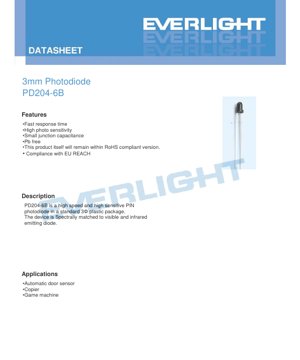
1. Product Overview
The PD204-6B is a high-performance silicon PIN photodiode designed for applications requiring fast response and high sensitivity to light in the visible and near-infrared spectrum. Housed in a standard 3mm diameter black plastic package, this device is engineered to provide reliable optical sensing capabilities. Its spectral response is specifically matched to complement visible and infrared emitting diodes (IREDs), making it an ideal receiver component in optoelectronic systems. The device is constructed with lead-free materials and complies with relevant environmental regulations, ensuring suitability for modern electronic manufacturing.
2. Key Features and Core Advantages
The PD204-6B distinguishes itself through several critical performance characteristics that cater to demanding sensing applications.
- Fast Response Time: The device exhibits a typical rise/fall time of 6 nanoseconds (under specified test conditions of VR=10V, RL=100Ω), enabling it to detect rapid changes in light intensity. This is crucial for applications involving data transmission, object detection, and timing-sensitive measurements.
- High Photo Sensitivity: With a typical short-circuit current (ISC) of 3.0 μA under an irradiance of 1 mW/cm² at 940nm, the photodiode provides a strong electrical signal from low light levels, improving signal-to-noise ratio and system reliability.
- Small Junction Capacitance: A low typical total capacitance (Ct) of 5 pF at VR=5V and 1MHz contributes to the fast response time and allows for operation in higher bandwidth circuits without significant signal degradation.
- Robust Construction: The device features a black lens, which helps minimize unwanted ambient light interference, and is packaged in a durable, industry-standard 3mm format.
- Environmental Compliance: The product is lead-free and designed to remain compliant with RoHS and EU REACH regulations, addressing global environmental and safety standards.
3. Technical Parameter Deep-Dive Analysis
Understanding the electrical and optical specifications is essential for proper circuit design and integration.
3.1 Absolute Maximum Ratings
These ratings define the limits beyond which permanent damage to the device may occur. Operation should always be maintained within these boundaries.
- Reverse Voltage (VR): 32 V. This is the maximum voltage that can be applied in reverse bias across the photodiode terminals.
- Power Dissipation (PC): 150 mW at or below 25°C free air temperature. This rating decreases with increasing ambient temperature, as shown in the derating curve.
- Operating Temperature (Topr): -40°C to +85°C. The device is specified to function correctly across this wide industrial temperature range.
- Storage Temperature (Tstg): -40°C to +100°C.
- Soldering Temperature (Tsol): 260°C. This guides the reflow soldering process parameters.
3.2 Electro-Optical Characteristics (Ta=25°C)
These parameters define the device's performance under normal operating conditions. Typical values represent the center of the distribution, while minimum and maximum values define the guaranteed limits.
- Spectral Response: The photodiode is sensitive across a range of approximately 840 nm to 1100 nm (at the 0.5 relative response points), with a peak sensitivity (λP) at 940 nm. This makes it perfectly suited for pairing with 940nm infrared LEDs.
- Photocurrent Generation:
- Short-Circuit Current (ISC): Typ. 3.0 μA at Ee=1mW/cm², λp=940nm. This is the current generated with zero voltage across the diode (photovoltaic mode).
- Reverse Light Current (IL): Min. 1.0 μA, Typ. 3.0 μA at Ee=1mW/cm², λp=940nm, VR=5V. This is the current when the diode is reverse-biased, which is the most common operating mode for speed and linearity.
- Dark Current (ID): Max. 10 nA at VR=10V, Ee=0mW/cm². This is the small leakage current that flows when no light is present. A low dark current is critical for detecting weak light signals.
- Open-Circuit Voltage (VOC): Typ. 0.42 V at Ee=1mW/cm², λp=940nm. This is the voltage generated across an open circuit under illumination.
- Capacitance (Ct): Typ. 5 pF at VR=5V, f=1MHz. This junction capacitance affects the RC time constant and thus the bandwidth of the sensing circuit.
- Response Speed (tr/tf): Typ. 6 ns at VR=10V, RL=100Ω. Defines how quickly the output current can follow a change in input light.
4. Performance Curve Analysis
Graphical data provides insight into how parameters vary with operating conditions.
4.1 Power Dissipation vs. Ambient Temperature
The derating curve shows that the maximum allowable power dissipation decreases linearly as the ambient temperature rises above 25°C. Designers must ensure the operating point (reverse voltage * photocurrent + dark current) does not exceed this curve to prevent thermal overload.
4.2 Spectral Sensitivity
The spectral response curve illustrates the relative sensitivity of the photodiode as a function of wavelength. It confirms the peak at 940nm and the useful bandwidth from approximately 840nm to 1100nm. The black lens material shapes this response, filtering some shorter wavelengths.
5. Mechanical and Package Information
The PD204-6B uses a standard radial-leaded, 3mm diameter package.
5.1 Package Dimensions
The dimensional drawing provides critical measurements for PCB footprint design and mechanical integration. Key dimensions include the overall diameter (3mm), lead spacing, lead diameter, and component height. All unspecified tolerances are ±0.25mm. The cathode is typically identified by a longer lead or a flat spot on the package rim.
5.2 Polarity Identification
Correct polarity is essential. The device is a diode. The anode is typically the shorter lead or the lead adjacent to the flat side of the package. Applying reverse bias (positive voltage to cathode, negative to anode) is the standard operating condition for photoconductive mode.
6. Soldering and Assembly Guidelines
- Reflow Soldering: The maximum soldering temperature is specified as 260°C. Standard infrared or convection reflow profiles for lead-free assemblies are applicable. The time above liquidus should be controlled according to industry standards to prevent package damage.
- Hand Soldering: If hand soldering is necessary, use a temperature-controlled iron. Limit contact time to less than 3 seconds per lead at a temperature not exceeding 350°C to avoid thermal stress on the plastic package and the internal semiconductor die.
- Cleaning: Use cleaning agents compatible with the black plastic epoxy material. Avoid ultrasonic cleaning unless verified to be safe for the component.
- Storage Conditions: Store in a dry, inert environment within the specified -40°C to +100°C temperature range. Use within 12 months from the date of shipment for guaranteed conformance to published specifications.
7. Packaging and Ordering Information
7.1 Packing Specification
The product is packed in anti-static bags. The standard packing quantity is 200 to 1000 pieces per bag. Four bags are packed into one inner carton, and one inner carton is shipped in one outside carton.
7.2 Label Information
The bag label contains essential traceability and product information, including the Part Number (P/N), quantity (QTY), lot number (LOT No.), and date code. The product is not binned or ranked for specific parameters like luminous intensity or wavelength; it is supplied to the standard electro-optical characteristic table.
8. Application Suggestions
8.1 Typical Application Circuits
The PD204-6B is commonly used in two primary circuit configurations:
- Photoconductive (Reverse-Bias) Mode: This is the preferred mode for high-speed and linear operation. A reverse bias voltage (e.g., 5V to 10V, staying below VR=32V) is applied. The photocurrent (IL) flows through a load resistor (RL). The voltage drop across RL is the output signal. A smaller RL gives faster response but lower voltage output. A transimpedance amplifier (TIA) is often used to convert the photocurrent to a voltage with high gain and bandwidth.
- Photovoltaic (Zero-Bias) Mode: The photodiode is connected directly to a high-impedance load (like an op-amp input). It generates a voltage (VOC) proportional to light intensity. This mode offers low noise but has slower response and is less linear.
8.2 Design Considerations
- Biasing: For best speed and linearity, operate in reverse bias. Ensure the bias voltage plus any signal voltage does not exceed the 32V maximum.
- Bandwidth and Load: The total capacitance (photodiode + amplifier input) and the load resistance/form the dominant pole limiting bandwidth (BW ≈ 1/(2πRC)). Choose RL or TIA feedback resistor accordingly.
- Ambient Light Rejection: The black lens helps, but for high ambient light environments, consider optical filtering (e.g., a 940nm bandpass filter) and modulating the IR source with synchronous detection.
- PCB Layout: Keep the photodiode close to the amplifier input to minimize stray capacitance and noise pickup. Use a ground plane for shielding. Bypass the bias supply with a capacitor close to the device.
9. Technical Comparison and Differentiation
Compared to phototransistors, the PD204-6B PIN photodiode offers significantly faster response times (nanoseconds vs. microseconds) and better linearity over a wide range of light intensity. It has no internal gain, which results in lower output current but also lower temperature dependence and more predictable performance. Compared to other photodiodes, its combination of 3mm package, 940nm peak sensitivity, 32V reverse voltage, and fast speed makes it a versatile choice for general-purpose IR sensing.
10. Frequently Asked Questions (FAQs)
Q: What is the difference between ISC and IL?
A: ISC (Short-Circuit Current) is measured with zero volts across the diode. IL (Reverse Light Current) is measured with a specified reverse bias voltage applied. IL is typically very close to ISC and is the parameter used for design in the common reverse-bias mode.
Q: How do I convert photocurrent to a usable voltage?
A: The simplest method is a load resistor (Vout = IL * RL). For better performance, use a transimpedance amplifier, which provides a low-impedance virtual ground at the photodiode cathode, maximizing speed and linearity, and gives Vout = -IL * Rfeedback.
Q: Can I use this with a visible light source?
A: Yes, but with reduced sensitivity. The spectral response curve shows it is sensitive down to visible wavelengths, but its peak is in the infrared. For optimal performance with a visible source, a photodiode with a peak in the visible spectrum (e.g., 550-650nm) would be more suitable.
Q: What is the purpose of the reverse breakdown voltage (VBR) test?
A: It is a quality and robustness test, indicating the voltage at which the diode enters avalanche breakdown. Normal operation should always be well below this value (typically using VR of 5V-10V).
11. Practical Application Examples
Example 1: Object Proximity Sensor in an Automatic Door. An IR LED (940nm) and the PD204-6B are placed on either side of a doorway. When the beam is uninterrupted, a steady photocurrent is detected. When a person breaks the beam, the drop in photocurrent triggers the door opening mechanism. The fast response of the PD204-6B ensures immediate detection.
Example 2: Paper Detection in a Copier. The photodiode can be used to detect the presence or absence of paper by reflecting an IR beam off the paper surface. The high sensitivity allows it to work with low-reflectivity papers, and the small package fits into tight spaces.
Example 3: Simple Data Link. By modulating an IR LED at a frequency within the photodiode's bandwidth (which can be several MHz with proper circuit design), the PD204-6B can be used for short-range, low-data-rate wireless communication, such as in remote controls or sensor telemetry.
12. Operating Principle
A PIN photodiode is a semiconductor device with a wide, lightly doped intrinsic (I) region sandwiched between P-type and N-type regions. When photons with energy greater than the semiconductor's bandgap are absorbed in the intrinsic region, they create electron-hole pairs. Under the influence of an internal built-in potential (in photovoltaic mode) or an applied reverse bias electric field (in photoconductive mode), these charge carriers are swept apart, generating a photocurrent that is proportional to the incident light intensity. The wide intrinsic region reduces junction capacitance (enabling high speed) and increases the volume for photon absorption (improving sensitivity).
13. Industry Trends and Context
Photodiodes like the PD204-6B are fundamental components in the growing field of optoelectronics and sensing. Trends include increasing integration with on-chip amplification and signal conditioning (e.g., in integrated optical sensors), demands for higher speed to support LiDAR and optical communications, and requirements for smaller package sizes for consumer electronics and IoT devices. There is also a continuous drive for improved performance over wider temperature ranges and lower power consumption. Devices with standard footprints and well-characterized performance, such as this one, remain essential for a vast array of industrial, commercial, and automotive sensing applications where reliability and cost-effectiveness are paramount.
Disclaimer: The information provided in this document is for technical reference. Designers should verify all parameters under their specific application conditions. Absolute maximum ratings must not be exceeded. The manufacturer assumes no liability for applications not in accordance with the provided specifications.
LED Specification Terminology
Complete explanation of LED technical terms
Photoelectric Performance
| Term | Unit/Representation | Simple Explanation | Why Important |
|---|---|---|---|
| Luminous Efficacy | lm/W (lumens per watt) | Light output per watt of electricity, higher means more energy efficient. | Directly determines energy efficiency grade and electricity cost. |
| Luminous Flux | lm (lumens) | Total light emitted by source, commonly called "brightness". | Determines if the light is bright enough. |
| Viewing Angle | ° (degrees), e.g., 120° | Angle where light intensity drops to half, determines beam width. | Affects illumination range and uniformity. |
| CCT (Color Temperature) | K (Kelvin), e.g., 2700K/6500K | Warmth/coolness of light, lower values yellowish/warm, higher whitish/cool. | Determines lighting atmosphere and suitable scenarios. |
| CRI / Ra | Unitless, 0–100 | Ability to render object colors accurately, Ra≥80 is good. | Affects color authenticity, used in high-demand places like malls, museums. |
| SDCM | MacAdam ellipse steps, e.g., "5-step" | Color consistency metric, smaller steps mean more consistent color. | Ensures uniform color across same batch of LEDs. |
| Dominant Wavelength | nm (nanometers), e.g., 620nm (red) | Wavelength corresponding to color of colored LEDs. | Determines hue of red, yellow, green monochrome LEDs. |
| Spectral Distribution | Wavelength vs intensity curve | Shows intensity distribution across wavelengths. | Affects color rendering and quality. |
Electrical Parameters
| Term | Symbol | Simple Explanation | Design Considerations |
|---|---|---|---|
| Forward Voltage | Vf | Minimum voltage to turn on LED, like "starting threshold". | Driver voltage must be ≥Vf, voltages add up for series LEDs. |
| Forward Current | If | Current value for normal LED operation. | Usually constant current drive, current determines brightness & lifespan. |
| Max Pulse Current | Ifp | Peak current tolerable for short periods, used for dimming or flashing. | Pulse width & duty cycle must be strictly controlled to avoid damage. |
| Reverse Voltage | Vr | Max reverse voltage LED can withstand, beyond may cause breakdown. | Circuit must prevent reverse connection or voltage spikes. |
| Thermal Resistance | Rth (°C/W) | Resistance to heat transfer from chip to solder, lower is better. | High thermal resistance requires stronger heat dissipation. |
| ESD Immunity | V (HBM), e.g., 1000V | Ability to withstand electrostatic discharge, higher means less vulnerable. | Anti-static measures needed in production, especially for sensitive LEDs. |
Thermal Management & Reliability
| Term | Key Metric | Simple Explanation | Impact |
|---|---|---|---|
| Junction Temperature | Tj (°C) | Actual operating temperature inside LED chip. | Every 10°C reduction may double lifespan; too high causes light decay, color shift. |
| Lumen Depreciation | L70 / L80 (hours) | Time for brightness to drop to 70% or 80% of initial. | Directly defines LED "service life". |
| Lumen Maintenance | % (e.g., 70%) | Percentage of brightness retained after time. | Indicates brightness retention over long-term use. |
| Color Shift | Δu′v′ or MacAdam ellipse | Degree of color change during use. | Affects color consistency in lighting scenes. |
| Thermal Aging | Material degradation | Deterioration due to long-term high temperature. | May cause brightness drop, color change, or open-circuit failure. |
Packaging & Materials
| Term | Common Types | Simple Explanation | Features & Applications |
|---|---|---|---|
| Package Type | EMC, PPA, Ceramic | Housing material protecting chip, providing optical/thermal interface. | EMC: good heat resistance, low cost; Ceramic: better heat dissipation, longer life. |
| Chip Structure | Front, Flip Chip | Chip electrode arrangement. | Flip chip: better heat dissipation, higher efficacy, for high-power. |
| Phosphor Coating | YAG, Silicate, Nitride | Covers blue chip, converts some to yellow/red, mixes to white. | Different phosphors affect efficacy, CCT, and CRI. |
| Lens/Optics | Flat, Microlens, TIR | Optical structure on surface controlling light distribution. | Determines viewing angle and light distribution curve. |
Quality Control & Binning
| Term | Binning Content | Simple Explanation | Purpose |
|---|---|---|---|
| Luminous Flux Bin | Code e.g., 2G, 2H | Grouped by brightness, each group has min/max lumen values. | Ensures uniform brightness in same batch. |
| Voltage Bin | Code e.g., 6W, 6X | Grouped by forward voltage range. | Facilitates driver matching, improves system efficiency. |
| Color Bin | 5-step MacAdam ellipse | Grouped by color coordinates, ensuring tight range. | Guarantees color consistency, avoids uneven color within fixture. |
| CCT Bin | 2700K, 3000K etc. | Grouped by CCT, each has corresponding coordinate range. | Meets different scene CCT requirements. |
Testing & Certification
| Term | Standard/Test | Simple Explanation | Significance |
|---|---|---|---|
| LM-80 | Lumen maintenance test | Long-term lighting at constant temperature, recording brightness decay. | Used to estimate LED life (with TM-21). |
| TM-21 | Life estimation standard | Estimates life under actual conditions based on LM-80 data. | Provides scientific life prediction. |
| IESNA | Illuminating Engineering Society | Covers optical, electrical, thermal test methods. | Industry-recognized test basis. |
| RoHS / REACH | Environmental certification | Ensures no harmful substances (lead, mercury). | Market access requirement internationally. |
| ENERGY STAR / DLC | Energy efficiency certification | Energy efficiency and performance certification for lighting. | Used in government procurement, subsidy programs, enhances competitiveness. |