Table of Contents
- 1. Product Overview
- 1.1 Core Advantages and Target Market
- 2. Technical Parameter Deep-Dive
- 2.1 Absolute Maximum Ratings
- 2.2 Electro-Optical Characteristics
- 2.2.1 Input Characteristics
- 2.2.2 Output Characteristics
- 2.2.3 Transfer Characteristics
- 3. Performance Curve Analysis
- 4. Mechanical and Package Information
- 4.1 Pin Configuration and Polarity
- 4.2 Package Dimensions
- 4.3 Recommended Pad Layout
- 4.4 Device Marking
- 5. Soldering and Assembly Guidelines
- 6. Packaging and Ordering Information
- 6.1 Ordering Code Structure
- 6.2 Packing Specifications
- 7. Application Suggestions
- 7.1 Typical Application Circuits
- 7.2 Design Considerations and Notes
- 8. Technical Comparison and Differentiation
- 9. Frequently Asked Questions (Based on Technical Parameters)
- 10. Practical Design Case Study
- 11. Operating Principle
- 12. Industry Trends
1. Product Overview
The EL8171-G Series represents a family of low-input current, general-purpose phototransistor photocouplers (optocouplers). Each device integrates an infrared emitting diode optically coupled to a silicon phototransistor detector, encapsulated within a 4-pin Dual In-line Package (DIP). The use of a green compound signifies compliance with halogen-free environmental standards. The primary function of this component is to provide electrical isolation and signal transmission between two circuits with different potentials or impedances, thereby preventing ground loops, voltage spikes, and noise from propagating across the isolation barrier.
1.1 Core Advantages and Target Market
The EL8171-G Series is designed for reliability and safety in industrial and consumer applications. Its key advantages include a high isolation voltage of 5000Vrms, which ensures robust protection against high-voltage transients. The current transfer ratio (CTR) range of 100% to 350% at a low input current (0.5mA) offers good sensitivity, allowing for efficient signal transfer with minimal drive requirements. Compliance with international safety standards (UL, cUL, VDE) and environmental directives (RoHS, Halogen-Free, REACH) makes it suitable for global markets. Target applications span programmable logic controllers (PLCs), system appliances, telecommunication equipment, measuring instruments, and various home appliances such as fan heaters, where reliable signal isolation is critical.
2. Technical Parameter Deep-Dive
This section provides an objective analysis of the device's electrical, optical, and thermal characteristics as defined in the datasheet.
2.1 Absolute Maximum Ratings
The Absolute Maximum Ratings define the stress limits beyond which permanent damage to the device may occur. These are not operating conditions.
- Input Forward Current (IF): 10 mA maximum. Exceeding this can destroy the infrared LED.
- Collector-Emitter Voltage (VCEO): 70 V maximum. This is the breakdown voltage limit for the output phototransistor.
- Total Power Dissipation (PTOT): 170 mW maximum. This is the sum of input (20 mW) and output (150 mW) power limits and is crucial for thermal management.
- Isolation Voltage (VISO): 5000 Vrms for 1 minute. This is a safety-critical rating tested under specific humidity conditions (40-60% RH) with input and output pins shorted separately.
- Operating Temperature (TOPR): -30°C to +100°C. This wide range supports use in harsh environments.
2.2 Electro-Optical Characteristics
These parameters are measured under typical conditions (Ta=25°C) and define the device's performance.
2.2.1 Input Characteristics
- Forward Voltage (VF): Typically 1.2V, with a maximum of 1.4V at IF=10mA. This is used to calculate the required series resistor for the input LED.
- Reverse Current (IR): Maximum 10 µA at VR=4V, indicating a low leakage when the LED is reverse-biased.
2.2.2 Output Characteristics
- Collector-Emitter Dark Current (ICEO): Maximum 100 nA at VCE=20V with IF=0mA. This is the leakage current of the phototransistor when no light is present, important for off-state signal integrity.
- Collector-Emitter Saturation Voltage (VCE(sat)): Maximum 0.2V at IF=10mA, IC=1mA. A low saturation voltage is desirable when the output is used as a switch to minimize voltage drop.
2.2.3 Transfer Characteristics
- Current Transfer Ratio (CTR): 100% (Min) to 350% (Max) at IF=0.5mA, VCE=5V. CTR = (IC / IF) * 100%. This wide range necessitates design consideration for gain tolerance. The test condition at a low 0.5mA input current highlights its suitability for low-power digital signal interfacing.
- Isolation Resistance (RIO): Minimum 5 x 10^10 Ω at VIO=500V DC. This extremely high resistance is key to the DC isolation performance.
- Rise/Fall Time (tr, tf): Maximum 18 µs each under specified test conditions (VCE=2V, IC=2mA, RL=100Ω). These parameters define the switching speed and bandwidth of the device, making it suitable for low-to-moderate frequency digital signals, not high-speed data transmission.
- Cut-off Frequency (fc): Typical 80 kHz. This -3dB bandwidth metric aligns with the rise/fall time specifications.
3. Performance Curve Analysis
While the provided PDF excerpt mentions typical curves but does not display them, standard photocoupler performance curves would typically include:
- CTR vs. Forward Current (IF): Shows how the current transfer ratio changes with the driving current of the LED. CTR often decreases at very high IF.
- CTR vs. Temperature: Illustrates the temperature dependence of the CTR, which typically decreases as temperature increases.
- Output Current (IC) vs. Collector-Emitter Voltage (VCE): Family of curves for different input currents (IF), showing the phototransistor's output characteristics similar to a bipolar transistor.
- Forward Voltage (VF) vs. Forward Current (IF): The IV characteristic of the input LED.
Designers should consult these curves (when available) to understand device behavior under non-standard conditions not covered in the table.
4. Mechanical and Package Information
The device is offered in several 4-pin DIP package variants to accommodate different assembly processes.
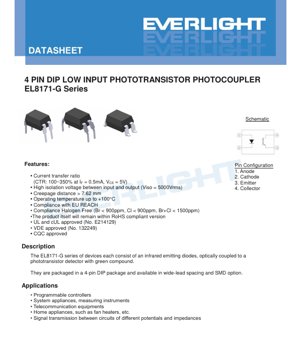
4.1 Pin Configuration and Polarity
The standard pinout is: 1. Anode, 2. Cathode (Input LED), 3. Emitter, 4. Collector (Output Phototransistor). Correct polarity must be observed during PCB layout and assembly.
4.2 Package Dimensions
The datasheet provides detailed mechanical drawings for four lead form options:
- Standard DIP: Through-hole package with standard lead spacing.
- Option M: Wide lead bend version with 0.4-inch (approx. 10.16mm) lead spacing for applications requiring greater creepage/clearance.
- Option S: Surface-mount (SMD) gull-wing lead form.
- Option S1: Surface-mount gull-wing lead form with a lower profile body height compared to Option S.
Critical dimensions include body size, lead pitch, standoff height, and overall footprint. These must be adhered to for proper PCB land pattern design.
4.3 Recommended Pad Layout
Separate recommended pad layouts are provided for the S and S1 surface-mount options. The datasheet notes these are for reference and may need modification based on specific PCB manufacturing processes and thermal requirements. The pad design affects solder joint reliability and self-alignment during reflow.
4.4 Device Marking
The top of the package is marked with a code: "EL" (manufacturer code), "8171" (device number), "G" (green/halogen-free), followed by a 1-digit year code (Y), a 2-digit week code (WW), and an optional "V" for VDE-approved versions. This allows for traceability of manufacturing date and variant.
5. Soldering and Assembly Guidelines
The Absolute Maximum Ratings specify a soldering temperature (TSOL) of 260°C for 10 seconds. This is a critical parameter for reflow or wave soldering processes.
- Reflow Soldering (for S/S1 options): A standard lead-free reflow profile with a peak temperature not exceeding 260°C and time above 240°C controlled to within the recommended limits (e.g., 10 seconds) should be used.
- Wave Soldering (for DIP/M options): Precautions should be taken to limit the exposure time of the device body to high temperature. Preheating is recommended to minimize thermal shock.
- Hand Soldering: Use a temperature-controlled iron and minimize contact time to prevent overheating the plastic package.
- Cleaning: Use cleaning agents compatible with the green epoxy compound.
- Storage: Devices should be stored in conditions within the storage temperature range (TSTG: -55°C to +125°C) and in moisture-sensitive packaging if intended for SMD assembly, following IPC/JEDEC standards to prevent "popcorning" during reflow.
6. Packaging and Ordering Information
6.1 Ordering Code Structure
The part number follows the pattern: EL8171X(Z)-VG
- X: Lead form option: None (Standard DIP), M (Wide lead), S (SMD), S1 (Low-profile SMD).
- Z: Tape and Reel option: None (tube), TA, TB, TU, TD (different reel types and quantities).
- V: Optional suffix denoting VDE safety approval.
- G: Denotes Halogen-Free (Green) compound.
6.2 Packing Specifications
The device is available in bulk tubes (100 units for through-hole parts) or on tape and reel for automated SMD assembly. The datasheet includes detailed tape dimensions (width, pocket size, pitch) and reel specifications for the various S and S1 tape options (TA, TB, TU, TD), which correspond to different quantities per reel (1000 or 1500 units).
7. Application Suggestions
7.1 Typical Application Circuits
The EL8171-G is commonly used in:
- Digital Signal Isolation: Isolating GPIO, UART, or other digital control lines between microcontrollers and power stages, sensors, or communication modules.
- Feedback Loop Isolation: In switch-mode power supplies (SMPS) to provide isolated voltage feedback from the secondary side to the primary side controller.
- Relay/Motor Driver Interface: Isolating low-voltage logic circuits from higher-voltage/higher-current driver stages to protect the logic controller.
- Noise Suppression: Breaking ground loops in analog signal chains or measurement systems.
7.2 Design Considerations and Notes
- Input Current Limiting: A series resistor (Rin) must always be used with the input LED to limit the forward current (IF) to a safe value below 10mA. Calculate Rin = (Vcc - VF) / IF, using the maximum VF from the datasheet for worst-case design.
- CTR Tolerance: The wide CTR range (100-350%) means the output current for a given input current can vary significantly from part to part. The circuit must function correctly across this entire range. For switching applications, ensure the minimum CTR provides sufficient output current to drive the load. For linear applications, feedback or trimming may be necessary.
- Speed Limitations: With maximum rise/fall times of 18 µs, the device is not suitable for high-speed data lines (e.g., USB, Ethernet). It is ideal for lower-frequency control signals (up to tens of kHz).
- Output Loading: The output phototransistor has a maximum collector current (IC) of 50mA and a power dissipation limit (PC) of 150mW. The load resistor (RL) connected between the collector and VCC must be chosen to keep the device within these limits under all operating conditions, considering VCE(sat) when on and VCEO when off.
- Creepage and Clearance: The specified creepage distance of >7.62mm contributes to the high isolation rating. PCB layout must maintain or exceed this distance between the input and output sides of the circuit, including traces and components.
8. Technical Comparison and Differentiation
Compared to basic photocouplers, the EL8171-G Series offers several differentiating features:
- High Isolation Voltage (5000Vrms): Exceeds the typical 2500Vrms or 3750Vrms found in many general-purpose couplers, offering enhanced safety for industrial equipment.
- Halogen-Free Compliance: Meets stringent environmental requirements, which is increasingly important for green electronics.
- Wide Lead Spacing Option (M): Provides a built-in solution for applications requiring increased PCB creepage distance without additional design effort.
- Low-Input Current Specification: The CTR is specified at a very low 0.5mA, indicating good sensitivity and suitability for power-efficient designs, whereas many competitors specify CTR at higher currents like 5mA or 10mA.
- Comprehensive Safety Approvals: UL, cUL, and VDE approvals streamline the certification process for end products targeting North American and European markets.
9. Frequently Asked Questions (Based on Technical Parameters)
Q1: How do I choose the input resistor value?
A1: Determine your desired forward current (IF), typically between 1mA and 10mA for good speed and CTR. Use the maximum forward voltage (VF_max = 1.4V) from the datasheet and your supply voltage (Vcc) to calculate the minimum resistor value: R_min = (Vcc - VF_max) / IF. Choose a standard resistor value equal to or greater than this to ensure IF is never exceeded.
Q2: My circuit doesn't work consistently across different batches of parts. Why?
A2: The most likely cause is the wide CTR tolerance (100-350%). A circuit designed to work with a high-CTR unit might fail with a low-CTR unit. Review your design to ensure it operates correctly at the minimum specified CTR. This may involve reducing the load on the output or increasing the input drive current.
Q3: Can I use this for analog signal isolation?
A3: While possible, it is challenging due to the non-linear CTR and its variation with temperature and current. For linear analog isolation, dedicated linear optocouplers or isolation amplifiers are recommended. This device is best suited for digital on/off switching.
Q4: What is the difference between Options S and S1?
A4: The primary difference is the package profile height. Option S1 has a lower body height than Option S. This is important for designs with strict vertical space constraints. Always check the mechanical drawings for exact dimensions.
10. Practical Design Case Study
Scenario: Isolating a 3.3V microcontroller GPIO pin to control a 12V relay coil with a resistance of 400Ω.
Design Steps:
- Input Side: Microcontroller GPIO is 3.3V. Target IF = 5mA for a good balance of speed and power.
VF_typ = 1.2V, VF_max = 1.4V.
R_in_min = (3.3V - 1.4V) / 0.005A = 380Ω. Select a standard 470Ω resistor.
Actual IF_typ = (3.3V - 1.2V) / 470Ω ≈ 4.5mA. - Output Side: Relay coil needs 12V / 400Ω = 30mA to energize. The photocoupler IC max is 50mA, so it's within limit.
At minimum CTR (100%), output current IC_min = IF * CTR_min = 4.5mA * 1.0 = 4.5mA. This is NOT enough to drive the 30mA relay.
Solution: Use the photocoupler to drive a transistor (e.g., a BJT or MOSFET), which then drives the relay coil. The photocoupler's output now only needs to provide base current to the transistor, which is much lower (e.g., 1-2mA). - Revised Output: With a transistor, target IC from photocoupler = 2mA.
At minimum CTR, required IF_min = IC / CTR_min = 2mA / 1.0 = 2mA. Our 4.5mA drive is sufficient.
Choose a pull-up resistor RL from collector to 12V. When on, VCE(sat) ~0.2V, so voltage across RL is ~11.8V. For IC=2mA, RL = 11.8V / 0.002A = 5.9kΩ. A 5.6kΩ or 6.2kΩ resistor would be suitable. - Check Power: Input power: P_in = VF * IF ≈ 1.2V * 0.0045A = 5.4mW (< 20mW limit). Output power when on: P_c = VCE(sat) * IC ≈ 0.2V * 0.002A = 0.4mW (< 150mW limit). Total power is well within the 170mW limit.
This case highlights the importance of considering worst-case CTR and using the photocoupler as a logic-level interface rather than a direct power switch for larger loads.
11. Operating Principle
A photocoupler operates on the principle of optical coupling to achieve electrical isolation. In the EL8171-G, an electrical current applied to the input side (pins 1 & 2) causes the infrared Light Emitting Diode (LED) to emit light. This light travels across a transparent insulating gap within the package and strikes the base region of a silicon phototransistor on the output side (pins 3 & 4). The incident light generates electron-hole pairs in the base, effectively acting as a base current, which allows a much larger collector current to flow between pins 4 and 3. The key is that the signal is transferred by light (photons) through an electrical insulator, breaking the metallic/galvanic connection between the two circuits. This provides excellent noise immunity and protects sensitive circuitry from high voltages or ground potential differences on the other side.
12. Industry Trends
The optocoupler market continues to evolve with several clear trends. There is a strong push towards higher integration, combining multiple isolation channels or integrating additional functions like I2C isolators or gate drivers into a single package. Speed is another critical area, with demand growing for digital isolators capable of supporting high-speed communication protocols (Mbps to Gbps range), which far exceed the capabilities of traditional phototransistor-based couplers like the EL8171-G. Furthermore, enhanced reliability and robustness are paramount, leading to improvements in isolation material technology (e.g., polyimide or SiO2 based digital isolators) and higher operating temperature ratings. Finally, the demand for miniaturization persists, driving the development of smaller surface-mount packages with the same or improved isolation ratings. Devices like the EL8171-G, with its SMD options and halogen-free compliance, address the environmental and assembly automation trends, while its core phototransistor technology remains the cost-effective and reliable solution for millions of medium-speed, high-isolation applications.
LED Specification Terminology
Complete explanation of LED technical terms
Photoelectric Performance
| Term | Unit/Representation | Simple Explanation | Why Important |
|---|---|---|---|
| Luminous Efficacy | lm/W (lumens per watt) | Light output per watt of electricity, higher means more energy efficient. | Directly determines energy efficiency grade and electricity cost. |
| Luminous Flux | lm (lumens) | Total light emitted by source, commonly called "brightness". | Determines if the light is bright enough. |
| Viewing Angle | ° (degrees), e.g., 120° | Angle where light intensity drops to half, determines beam width. | Affects illumination range and uniformity. |
| CCT (Color Temperature) | K (Kelvin), e.g., 2700K/6500K | Warmth/coolness of light, lower values yellowish/warm, higher whitish/cool. | Determines lighting atmosphere and suitable scenarios. |
| CRI / Ra | Unitless, 0–100 | Ability to render object colors accurately, Ra≥80 is good. | Affects color authenticity, used in high-demand places like malls, museums. |
| SDCM | MacAdam ellipse steps, e.g., "5-step" | Color consistency metric, smaller steps mean more consistent color. | Ensures uniform color across same batch of LEDs. |
| Dominant Wavelength | nm (nanometers), e.g., 620nm (red) | Wavelength corresponding to color of colored LEDs. | Determines hue of red, yellow, green monochrome LEDs. |
| Spectral Distribution | Wavelength vs intensity curve | Shows intensity distribution across wavelengths. | Affects color rendering and quality. |
Electrical Parameters
| Term | Symbol | Simple Explanation | Design Considerations |
|---|---|---|---|
| Forward Voltage | Vf | Minimum voltage to turn on LED, like "starting threshold". | Driver voltage must be ≥Vf, voltages add up for series LEDs. |
| Forward Current | If | Current value for normal LED operation. | Usually constant current drive, current determines brightness & lifespan. |
| Max Pulse Current | Ifp | Peak current tolerable for short periods, used for dimming or flashing. | Pulse width & duty cycle must be strictly controlled to avoid damage. |
| Reverse Voltage | Vr | Max reverse voltage LED can withstand, beyond may cause breakdown. | Circuit must prevent reverse connection or voltage spikes. |
| Thermal Resistance | Rth (°C/W) | Resistance to heat transfer from chip to solder, lower is better. | High thermal resistance requires stronger heat dissipation. |
| ESD Immunity | V (HBM), e.g., 1000V | Ability to withstand electrostatic discharge, higher means less vulnerable. | Anti-static measures needed in production, especially for sensitive LEDs. |
Thermal Management & Reliability
| Term | Key Metric | Simple Explanation | Impact |
|---|---|---|---|
| Junction Temperature | Tj (°C) | Actual operating temperature inside LED chip. | Every 10°C reduction may double lifespan; too high causes light decay, color shift. |
| Lumen Depreciation | L70 / L80 (hours) | Time for brightness to drop to 70% or 80% of initial. | Directly defines LED "service life". |
| Lumen Maintenance | % (e.g., 70%) | Percentage of brightness retained after time. | Indicates brightness retention over long-term use. |
| Color Shift | Δu′v′ or MacAdam ellipse | Degree of color change during use. | Affects color consistency in lighting scenes. |
| Thermal Aging | Material degradation | Deterioration due to long-term high temperature. | May cause brightness drop, color change, or open-circuit failure. |
Packaging & Materials
| Term | Common Types | Simple Explanation | Features & Applications |
|---|---|---|---|
| Package Type | EMC, PPA, Ceramic | Housing material protecting chip, providing optical/thermal interface. | EMC: good heat resistance, low cost; Ceramic: better heat dissipation, longer life. |
| Chip Structure | Front, Flip Chip | Chip electrode arrangement. | Flip chip: better heat dissipation, higher efficacy, for high-power. |
| Phosphor Coating | YAG, Silicate, Nitride | Covers blue chip, converts some to yellow/red, mixes to white. | Different phosphors affect efficacy, CCT, and CRI. |
| Lens/Optics | Flat, Microlens, TIR | Optical structure on surface controlling light distribution. | Determines viewing angle and light distribution curve. |
Quality Control & Binning
| Term | Binning Content | Simple Explanation | Purpose |
|---|---|---|---|
| Luminous Flux Bin | Code e.g., 2G, 2H | Grouped by brightness, each group has min/max lumen values. | Ensures uniform brightness in same batch. |
| Voltage Bin | Code e.g., 6W, 6X | Grouped by forward voltage range. | Facilitates driver matching, improves system efficiency. |
| Color Bin | 5-step MacAdam ellipse | Grouped by color coordinates, ensuring tight range. | Guarantees color consistency, avoids uneven color within fixture. |
| CCT Bin | 2700K, 3000K etc. | Grouped by CCT, each has corresponding coordinate range. | Meets different scene CCT requirements. |
Testing & Certification
| Term | Standard/Test | Simple Explanation | Significance |
|---|---|---|---|
| LM-80 | Lumen maintenance test | Long-term lighting at constant temperature, recording brightness decay. | Used to estimate LED life (with TM-21). |
| TM-21 | Life estimation standard | Estimates life under actual conditions based on LM-80 data. | Provides scientific life prediction. |
| IESNA | Illuminating Engineering Society | Covers optical, electrical, thermal test methods. | Industry-recognized test basis. |
| RoHS / REACH | Environmental certification | Ensures no harmful substances (lead, mercury). | Market access requirement internationally. |
| ENERGY STAR / DLC | Energy efficiency certification | Energy efficiency and performance certification for lighting. | Used in government procurement, subsidy programs, enhances competitiveness. |