1. Product Overview
The EL354N-G series represents a family of compact, high-performance phototransistor photocouplers designed specifically for AC input applications. These devices are engineered to provide reliable electrical isolation and signal transmission in environments where input polarity may be unknown or alternating. The core of the device consists of two infrared emitting diodes connected in inverse parallel, optically coupled to a silicon phototransistor detector. This unique configuration allows the device to respond to current flow in either direction through the input LEDs, making it inherently suitable for AC signal monitoring and sensing applications where DC polarity is not fixed.
Packaged in a space-saving 4-pin Small Outline Package (SOP), these photocouplers are ideal for modern, high-density printed circuit board (PCB) designs. A key design philosophy behind this series is compliance with global environmental and safety standards. The devices are halogen-free, adhering to strict limits on bromine (Br < 900 ppm), chlorine (Cl < 900 ppm), and their combined total (Br+Cl < 1500 ppm). Furthermore, they maintain compliance with RoHS (Restriction of Hazardous Substances) directives and the EU REACH regulation, ensuring they meet contemporary environmental requirements for electronic components.
1.1 Core Advantages and Target Market
The primary advantage of the EL354N-G series lies in its combination of AC input capability, high isolation, and compact form factor. The high isolation voltage of 3750 Vrms between input and output provides a robust safety barrier, protecting sensitive low-voltage control circuits from high-voltage mains or noisy industrial lines. This makes them indispensable in applications requiring galvanic isolation.
The target markets for this component are diverse, spanning industrial automation, telecommunications, and power management. Key application areas include AC line monitoring in power supplies and appliances, providing input isolation in programmable logic controllers (PLCs), interfacing in telephone line circuits, and serving as sensors for DC signals of unknown polarity. The device's approvals from major international safety agencies—including UL, cUL, VDE, SEMKO, NEMKO, DEMKO, FIMKO, and CQC—facilitate its use in end products destined for global markets, simplifying the certification process for equipment manufacturers.
2. In-Depth Technical Parameter Analysis
A thorough understanding of the device's limits and performance characteristics is crucial for reliable circuit design. The parameters define the operational envelope and ensure the component is used within its safe operating area (SOA).
2.1 Absolute Maximum Ratings
The Absolute Maximum Ratings specify the stress limits beyond which permanent damage to the device may occur. These are not operating conditions.
- Input Forward Current (IF): ±50 mA (DC). This rating applies to current in either direction through the input diodes.
- Peak Forward Current (IFP): 1 A for a 1 µs pulse. This allows the device to withstand brief current surges.
- Power Dissipation: The total device power dissipation (PTOT) must not exceed 200 mW. The input side (PD) is rated for 70 mW with a derating factor of 3.7 mW/°C above 90°C ambient temperature (Ta). The output side (PC) is rated for 150 mW, derating above 70°C Ta.
- Voltage Ratings: The collector-emitter voltage (VCEO) is 80 V, while the emitter-collector voltage (VECO) is 6 V. The asymmetry is due to the phototransistor's structure.
- Isolation Voltage (VISO): 3750 Vrms for 1 minute at 40-60% relative humidity. This is a critical safety parameter.
- Temperature Range: Operating temperature (TOPR) spans from -55°C to +100°C. Storage temperature (TSTG) ranges from -55°C to +125°C.
- Soldering Temperature: The device can withstand a peak soldering temperature (TSOL) of 260°C for 10 seconds, which is compatible with lead-free reflow processes.
2.2 Electro-Optical Characteristics
These parameters define the device's performance under normal operating conditions at 25°C, unless otherwise specified.
2.2.1 Input Characteristics
- Forward Voltage (VF): Typically 1.2 V, with a maximum of 1.4 V at a forward current (IF) of ±20 mA. This low voltage drop is beneficial for low-power circuits.
- Input Capacitance (Cin): Ranges from 50 pF (typical) to 250 pF (max) at 1 kHz. This parameter affects high-frequency response and potential coupling noise.
2.2.2 Output Characteristics
- Dark Current (ICEO): The leakage current from collector to emitter when the input LED is off (IF=0) and VCE=20V is a maximum of 100 nA. A low dark current is essential for good signal-to-noise ratio in off-state conditions.
- Breakdown Voltages: BVCEO is a minimum of 80 V, and BVECO is a minimum of 7 V. These define the maximum sustainable reverse voltages.
2.2.3 Transfer Characteristics
These parameters describe the coupling efficiency and speed between the input and output.
- Current Transfer Ratio (CTR): This is the ratio of output collector current (IC) to input forward current (IF), expressed as a percentage. It is the key parameter for gain. The standard EL354N has a CTR range of 20% to 300% at IF = ±1mA, VCE = 5V. The EL354NA variant offers a tighter, higher bin with a CTR range of 50% to 150% under the same conditions. This binning allows designers to select devices for more consistent gain in production.
- Saturation Voltage (VCE(sat)): Typically 0.1 V, maximum 0.2 V when IF=±20mA and IC=1mA. A low saturation voltage minimizes power loss when the output transistor is fully on.
- Isolation Resistance (RIO): Minimum 5×10¹⁰ Ω, typical 1011 Ω at 500 V DC. This extremely high resistance is fundamental to the isolation function.
- Cut-off Frequency (fc): Typically 80 kHz (-3dB point) under specified test conditions. This defines the maximum useful signal frequency.
- Floating Capacitance (CIO): Typically 0.6 pF, maximum 1.0 pF at 1 MHz. This is the parasitic capacitance across the isolation barrier, which can couple high-frequency noise.
- Switching Speed: Both rise time (tr) and fall time (tf) are specified as a maximum of 18 µs. This relatively moderate speed is suitable for line-frequency monitoring (50/60 Hz) and many industrial control signals, but not for high-speed digital communication.
3. Performance Curve Analysis
While the datasheet references typical electro-optical characteristic curves, their specific plots (e.g., CTR vs. Temperature, CTR vs. Forward Current) are essential for detailed design. These curves typically show that CTR decreases with increasing ambient temperature and may have a non-linear relationship with forward current. Designers must consult these graphs to derate performance appropriately for their specific operating environment, ensuring the circuit maintains sufficient gain across the intended temperature range. The relationship between output current and forward current is also critical for determining the required drive current to achieve a desired output state, especially when operating near the limits of the CTR specification.
4. Mechanical, Package, and Assembly Information
4.1 Package Dimensions and Polarity
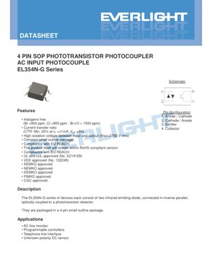
The device is housed in a 4-pin SOP package. The pin configuration is as follows: Pin 1 is Anode/Cathode, Pin 2 is Cathode/Anode (for the inverse-parallel LED pair), Pin 3 is the Emitter of the phototransistor, and Pin 4 is the Collector. This pinout is crucial for correct PCB layout. The package drawing provides precise mechanical dimensions including body length, width, height, lead pitch, and lead dimensions, which must be adhered to for accurate PCB footprint design.
4.2 Recommended PCB Pad Layout
A suggested surface-mount pad layout is provided. It is emphasized that this is a reference design and should be modified based on individual manufacturing processes, PCB material, and thermal requirements. The goal of the pad design is to ensure reliable solder joint formation during reflow while managing thermal stress on the component.
4.3 Soldering and Reflow Guidelines
Detailed reflow soldering conditions are specified, referencing IPC/JEDEC J-STD-020D. The profile is critical for lead-free assembly:
- Preheat: 150°C to 200°C over 60-120 seconds.
- Ramp-up: Maximum 3°C/second from 200°C to peak.
- Time Above Liquidus (217°C): 60-100 seconds.
- Peak Temperature: 260°C maximum.
- Time within 5°C of Peak: 30 seconds maximum.
- Cooling Rate: Maximum 6°C/second.
- Total Cycle Time: 25°C to peak in 8 minutes max.
- Reflow Passes: The device can withstand a maximum of 3 reflow cycles.
Adhering to this profile prevents thermal damage to the plastic package and the internal wire bonds.
5. Ordering, Packaging, and Marking
5.1 Part Numbering and Binning System
The part number follows the structure: EL354N(X)(Y)-VG.
- X: CTR Rank option. 'A' denotes the 50-150% bin (EL354NA). No letter denotes the standard 20-300% bin (EL354N).
- Y: Tape and Reel option. 'TA' or 'TB' specifies reel type and orientation. Omission indicates tube packaging (100 units).
- V: Optional suffix denoting VDE approval is included.
- G: Denotes Halogen-free construction.
Packaging options include tubes (100 units) or tape-and-reel (3000 units per reel for both TA and TB options). The 'TA' and 'TB' options differ in the orientation of the components on the carrier tape, which must match the pick-and-place machine's feeder requirements.
5.2 Device Marking
Devices are marked on the top surface with a code: EL 354N RYWWV.
- EL: Manufacturer code.
- 354N: Base device number.
- R: CTR Rank (e.g., 'A' or blank).
- Y: 1-digit year code.
- WW: 2-digit week code.
- V: Presence indicates VDE approval (optional).
5.3 Tape and Reel Specifications
Detailed dimensions for the embossed carrier tape are provided, including pocket dimensions (A, B, D0, D1), tape width (W), pitch (P0), and cover tape seal dimensions. These are necessary for setting up automated assembly equipment correctly.
6. Application Guidelines and Design Considerations
6.1 Typical Application Circuits
The primary application is AC line voltage sensing or zero-crossing detection. A typical circuit involves connecting the input pins (1 & 2) in series with a current-limiting resistor across the AC line. The resistor value must be calculated to limit the peak forward current (IF) to a safe value below 50 mA, considering the peak AC voltage. The output transistor can be connected in a common-emitter configuration (Emitter to ground, Collector pulled up through a load resistor to a logic supply) to provide a digital signal that toggles with the AC cycle. For unknown-polarity DC sensing, the device can be placed directly in the sensing line, as it will conduct regardless of current direction.
6.2 Critical Design Factors
- Current Limiting: The most critical aspect of input circuit design. The resistor must limit current under worst-case conditions (maximum line voltage, minimum resistor tolerance).
- CTR Degradation: CTR can degrade over time, especially at high operating temperatures and currents. Design should incorporate a margin (e.g., use minimum CTR from datasheet and then apply a further derating factor for lifetime).
- Noise Immunity: The parasitic capacitance (CIO) can couple high-frequency transients (like ESD or EMI) across the isolation barrier. In noisy environments, additional filtering on the output side or the use of a faster digital filter in the microcontroller may be necessary.
- Switching Speed Limitation: The 18 µs rise/fall time limits the device to lower-frequency applications. It is not suitable for isolating high-speed digital data lines.
- Heat Dissipation Ensure the total power dissipation (input LED loss + output transistor loss) does not exceed 200 mW, considering derating with temperature.
7. Technical Comparison and Differentiation
The EL354N-G's key differentiator is its integrated inverse-parallel LED input, eliminating the need for external bridge rectifiers or complex circuitry to handle AC or unknown-polarity DC signals. Compared to standard DC-input photocouplers, this simplifies the BOM and saves board space. Within the AC-input photocoupler segment, its combination of 3750Vrms isolation, halogen-free material, and comprehensive international safety approvals (UL, VDE, etc.) in a compact SOP package presents a strong value proposition for cost-sensitive yet safety-critical global applications. The availability of a tighter CTR bin (EL354NA) offers an advantage for designs requiring more consistent gain without manual sorting or calibration.
8. Frequently Asked Questions (FAQs)
Q: Can I use this device to directly sense 120VAC or 230VAC mains?
A: Yes, but you must use an external series current-limiting resistor. Calculate its value based on the peak mains voltage (e.g., 230VAC RMS has a peak of ~325V) and the desired LED current, ensuring the peak current stays well below the Absolute Maximum Rating of 50 mA.
Q: What is the difference between the EL354N and EL354NA?
A: The difference is in the Current Transfer Ratio (CTR) binning. The EL354N has a wider range (20-300%), while the EL354NA has a tighter, higher minimum range (50-150%). Use the 'NA' version for applications requiring more consistent gain from unit to unit.
Q: The output is a phototransistor. Can I use it to directly drive a relay?
A: It is not recommended. The phototransistor's current handling is limited (related to its power dissipation rating). It is designed as a signal-level device. To drive a relay, use the photocoupler output to drive a larger power transistor or a MOSFET gate.
Q: How do I ensure reliable isolation in my design?
A: Maintain proper creepage and clearance distances on the PCB between the input and output circuits as per the relevant safety standard (e.g., IEC 60950-1, IEC 62368-1). The 3750Vrms rating of the component itself must be supported by adequate spacing on the board.
9. Operational Principle
The device operates on the principle of optoelectronic conversion and isolation. When a current flows through either of the two input infrared LEDs (depending on polarity), it emits light. This light traverses a transparent isolation barrier (typically a molded plastic) and strikes the base region of the silicon phototransistor on the output side. The photons generate electron-hole pairs in the base, effectively acting as a base current, which turns the transistor on, allowing a much larger collector current to flow. The key is that the only connection between input and output is optical, providing the galvanic isolation. The inverse-parallel LED configuration means that current flowing into Pin 1 (Anode) and out of Pin 2 (Cathode) lights one LED, while current in the opposite direction lights the other LED, ensuring operation with AC or bidirectional DC.
10. Industry Trends
The trend in optocouplers and isolation technology is towards higher integration, faster speeds, and lower power consumption. While traditional phototransistor-based couplers like the EL354N-G remain vital for cost-effective, medium-speed isolation in power and industrial controls, newer technologies are emerging. These include digital isolators based on CMOS technology and RF coupling, which offer significantly higher data rates, lower power, and higher reliability. However, for basic AC line sensing and voltage monitoring where simplicity, high isolation voltage, and proven robustness are paramount, phototransistor AC couplers continue to be a preferred and reliable solution. The move towards halogen-free and enhanced environmental compliance, as seen in the '-G' series, is a direct response to global regulatory trends.
LED Specification Terminology
Complete explanation of LED technical terms
Photoelectric Performance
| Term | Unit/Representation | Simple Explanation | Why Important |
|---|---|---|---|
| Luminous Efficacy | lm/W (lumens per watt) | Light output per watt of electricity, higher means more energy efficient. | Directly determines energy efficiency grade and electricity cost. |
| Luminous Flux | lm (lumens) | Total light emitted by source, commonly called "brightness". | Determines if the light is bright enough. |
| Viewing Angle | ° (degrees), e.g., 120° | Angle where light intensity drops to half, determines beam width. | Affects illumination range and uniformity. |
| CCT (Color Temperature) | K (Kelvin), e.g., 2700K/6500K | Warmth/coolness of light, lower values yellowish/warm, higher whitish/cool. | Determines lighting atmosphere and suitable scenarios. |
| CRI / Ra | Unitless, 0–100 | Ability to render object colors accurately, Ra≥80 is good. | Affects color authenticity, used in high-demand places like malls, museums. |
| SDCM | MacAdam ellipse steps, e.g., "5-step" | Color consistency metric, smaller steps mean more consistent color. | Ensures uniform color across same batch of LEDs. |
| Dominant Wavelength | nm (nanometers), e.g., 620nm (red) | Wavelength corresponding to color of colored LEDs. | Determines hue of red, yellow, green monochrome LEDs. |
| Spectral Distribution | Wavelength vs intensity curve | Shows intensity distribution across wavelengths. | Affects color rendering and quality. |
Electrical Parameters
| Term | Symbol | Simple Explanation | Design Considerations |
|---|---|---|---|
| Forward Voltage | Vf | Minimum voltage to turn on LED, like "starting threshold". | Driver voltage must be ≥Vf, voltages add up for series LEDs. |
| Forward Current | If | Current value for normal LED operation. | Usually constant current drive, current determines brightness & lifespan. |
| Max Pulse Current | Ifp | Peak current tolerable for short periods, used for dimming or flashing. | Pulse width & duty cycle must be strictly controlled to avoid damage. |
| Reverse Voltage | Vr | Max reverse voltage LED can withstand, beyond may cause breakdown. | Circuit must prevent reverse connection or voltage spikes. |
| Thermal Resistance | Rth (°C/W) | Resistance to heat transfer from chip to solder, lower is better. | High thermal resistance requires stronger heat dissipation. |
| ESD Immunity | V (HBM), e.g., 1000V | Ability to withstand electrostatic discharge, higher means less vulnerable. | Anti-static measures needed in production, especially for sensitive LEDs. |
Thermal Management & Reliability
| Term | Key Metric | Simple Explanation | Impact |
|---|---|---|---|
| Junction Temperature | Tj (°C) | Actual operating temperature inside LED chip. | Every 10°C reduction may double lifespan; too high causes light decay, color shift. |
| Lumen Depreciation | L70 / L80 (hours) | Time for brightness to drop to 70% or 80% of initial. | Directly defines LED "service life". |
| Lumen Maintenance | % (e.g., 70%) | Percentage of brightness retained after time. | Indicates brightness retention over long-term use. |
| Color Shift | Δu′v′ or MacAdam ellipse | Degree of color change during use. | Affects color consistency in lighting scenes. |
| Thermal Aging | Material degradation | Deterioration due to long-term high temperature. | May cause brightness drop, color change, or open-circuit failure. |
Packaging & Materials
| Term | Common Types | Simple Explanation | Features & Applications |
|---|---|---|---|
| Package Type | EMC, PPA, Ceramic | Housing material protecting chip, providing optical/thermal interface. | EMC: good heat resistance, low cost; Ceramic: better heat dissipation, longer life. |
| Chip Structure | Front, Flip Chip | Chip electrode arrangement. | Flip chip: better heat dissipation, higher efficacy, for high-power. |
| Phosphor Coating | YAG, Silicate, Nitride | Covers blue chip, converts some to yellow/red, mixes to white. | Different phosphors affect efficacy, CCT, and CRI. |
| Lens/Optics | Flat, Microlens, TIR | Optical structure on surface controlling light distribution. | Determines viewing angle and light distribution curve. |
Quality Control & Binning
| Term | Binning Content | Simple Explanation | Purpose |
|---|---|---|---|
| Luminous Flux Bin | Code e.g., 2G, 2H | Grouped by brightness, each group has min/max lumen values. | Ensures uniform brightness in same batch. |
| Voltage Bin | Code e.g., 6W, 6X | Grouped by forward voltage range. | Facilitates driver matching, improves system efficiency. |
| Color Bin | 5-step MacAdam ellipse | Grouped by color coordinates, ensuring tight range. | Guarantees color consistency, avoids uneven color within fixture. |
| CCT Bin | 2700K, 3000K etc. | Grouped by CCT, each has corresponding coordinate range. | Meets different scene CCT requirements. |
Testing & Certification
| Term | Standard/Test | Simple Explanation | Significance |
|---|---|---|---|
| LM-80 | Lumen maintenance test | Long-term lighting at constant temperature, recording brightness decay. | Used to estimate LED life (with TM-21). |
| TM-21 | Life estimation standard | Estimates life under actual conditions based on LM-80 data. | Provides scientific life prediction. |
| IESNA | Illuminating Engineering Society | Covers optical, electrical, thermal test methods. | Industry-recognized test basis. |
| RoHS / REACH | Environmental certification | Ensures no harmful substances (lead, mercury). | Market access requirement internationally. |
| ENERGY STAR / DLC | Energy efficiency certification | Energy efficiency and performance certification for lighting. | Used in government procurement, subsidy programs, enhances competitiveness. |