Table of Contents
- 1. Product Overview
- 2. In-Depth Technical Parameter Analysis
- 2.1 Absolute Maximum Ratings
- 2.2 Electro-Optical Characteristics
- 3. Performance Curve Analysis
- 4. Mechanical, Package, and Assembly Information
- 4.1 Pin Configuration and Package Dimensions
- 4.2 Soldering and Assembly Guidelines
- 5. Ordering, Packaging, and Marking
- 5.1 Part Numbering System
- 5.2 Packaging Specifications
- 5.3 Device Marking
- 6. Application Notes and Design Considerations
- 6.1 Typical Applications
- 6.2 Critical Design Considerations
- 7. Technical Comparison and Positioning
- 8. Frequently Asked Questions (FAQ)
- 8.1 What is the difference between the TA and TB tape options?
- 8.2 How do I choose between the B, C, and BC CTR grades?
- 8.3 Can this device be used for analog signal isolation?
- 8.4 What is the purpose of the isolation voltage test (pins 1-2 shorted to 3-4)?
1. Product Overview
The EL121N series represents a family of infrared optoelectronic components designed for signal isolation and transmission. At its core, it consists of a gallium arsenide infrared light-emitting diode (IRED) optically coupled to a silicon NPN phototransistor, all housed within a compact, surface-mount 4-pin Small Outline Package (SOP). The primary function is to transfer electrical signals between two circuits while maintaining high electrical isolation, thereby preventing noise, ground loops, and voltage spikes from propagating from one side to the other.
The device is engineered for applications requiring reliable isolation in constrained spaces. Its 2.0mm low profile makes it suitable for modern, high-density printed circuit board (PCB) designs. A key design philosophy behind this series is compliance with global environmental and safety standards, including being halogen-free, lead-free (Pb-free), and compliant with RoHS and EU REACH directives. Furthermore, it carries significant international safety approvals, including UL, cUL, VDE, SEMKO, NEMKO, DEMKO, and FIMKO, which underscores its reliability and suitability for use in commercial and industrial equipment worldwide.
2. In-Depth Technical Parameter Analysis
2.1 Absolute Maximum Ratings
These ratings define the stress limits beyond which permanent damage to the device may occur. Operation under or at these limits is not guaranteed.
- Input (LED Side): The forward current (
I_F) is rated at 50mA continuous. A brief peak forward current (I_FP) of 1A for 1 microsecond is permissible, which is relevant for pulsed operation. The maximum reverse voltage (V_R) is 6V, emphasizing the need for proper polarity protection. - Output (Transistor Side): The collector current (
I_C) is rated at 50mA. The collector-emitter voltage (V_CEO) is 80V, while the emitter-collector voltage (V_ECO) is only 7V, highlighting the asymmetric nature of the phototransistor's breakdown characteristics. - Power and Thermal: The total device power dissipation (
P_TOT) is 200mW. Separate derating factors are provided: 2.9 mW/°C for the input (LED) above 100°C ambient, and 3.7 mW/°C for the output (transistor) above 70°C ambient. This is critical for thermal management in high-temperature environments. - Isolation and Environment: The isolation voltage (
V_ISO) is 3750 Vrms for 1 minute, tested with pins 1-2 shorted together and pins 3-4 shorted together. The operating temperature range is -55°C to +110°C, and storage extends to -55°C to +125°C.
2.2 Electro-Optical Characteristics
These parameters define the device's performance under normal operating conditions (Ta=25°C unless noted).
- Input Characteristics: The forward voltage (
V_F) is typically 1.2V at a test current of 20mA, with a maximum of 1.4V. This low voltage is beneficial for low-power logic interface circuits. The reverse leakage current (I_R) is a maximum of 10µA at 4V. - Output Characteristics: The collector-emitter dark current (
I_CEO), which is the leakage current with the LED off, is a maximum of 100nA at VCE=20V. The breakdown voltages (BV_CEO=80V,BV_ECO=7V) confirm the ratings. - Transfer Characteristics: This is the heart of the device's specification.
- Current Transfer Ratio (CTR): This is the ratio of output collector current to input LED forward current, expressed as a percentage. The EL121N series offers a grading/binning system:
- EL121N (Standard): CTR range 50% to 400% at IF=5mA, VCE=5V.
- EL121N B: A tighter bin of 130% to 260%.
- EL121N C: A higher-performance bin of 200% to 400%.
- EL121N BC: A broad bin covering 130% to 400%.
- Saturation Voltage (
V_CE(sat)): Typically 0.1V (max 0.2V) when driven with IF=20mA and loaded with IC=1mA. This low value is excellent for digital switching applications, minimizing voltage loss. - Isolation Resistance (
R_IO): Minimum 5 x 10¹⁰ Ω, indicating extremely high DC insulation resistance. - Switching Speed: Rise time (
t_r) is typically 6µs (max 18µs) and fall time (t_f) is typically 8µs (max 18µs) under specified test conditions (VCE=2V, IC=2mA, RL=100Ω). This defines the device's capability for medium-speed digital signal transmission.
- Current Transfer Ratio (CTR): This is the ratio of output collector current to input LED forward current, expressed as a percentage. The EL121N series offers a grading/binning system:
3. Performance Curve Analysis
The datasheet references typical electro-optical characteristic curves. While the specific graphs are not reproduced in text, they typically include the following relationships which are crucial for design:
- CTR vs. Forward Current (IF): CTR is not constant; it generally decreases as IF increases. Designers must consult this curve to choose an operating point that provides the desired gain without overdriving the LED.
- CTR vs. Ambient Temperature (Ta): The CTR of optocouplers has a negative temperature coefficient; it decreases as temperature increases. This curve is vital for ensuring circuit stability over the intended operating temperature range.
- Collector Current vs. Collector-Emitter Voltage (IC-VCE): These output characteristic curves show the phototransistor operating in its linear (active) and saturated regions, similar to a standard bipolar transistor, but with IF as the control parameter instead of base current.
- Forward Voltage vs. Forward Current (VF-IF): This LED characteristic is important for designing the current-limiting driver circuit.
Figure 10 in the datasheet provides the standard test circuit and waveform definitions for measuring switching times (t_on, t_off, t_r, t_f), using a resistive load (RL) and a defined input pulse.
4. Mechanical, Package, and Assembly Information
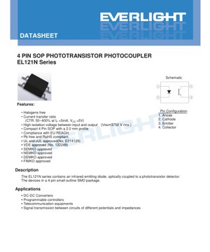
4.1 Pin Configuration and Package Dimensions
The 4-pin SOP package has a clear pinout:
- Anode (A) of the infrared LED
- Cathode (K) of the infrared LED
- Emitter (E) of the phototransistor
- Collector (C) of the phototransistor
4.2 Soldering and Assembly Guidelines
The device is rated for a maximum soldering temperature (T_SOL) of 260°C for 10 seconds. Furthermore, a detailed reflow soldering profile is provided, compliant with IPC/JEDEC J-STD-020D. Key parameters of this profile include:
- Preheat: 150°C to 200°C over 60-120 seconds.
- Time Above Liquidus (217°C): 60-100 seconds.
- Peak Temperature: 260°C maximum.
- Time within 5°C of Peak: 30 seconds maximum.
- Maximum Number of Reflows: 3 times.
5. Ordering, Packaging, and Marking
5.1 Part Numbering System
The part number follows the format: EL121N(X)(Y)-V
- EL121N: Base device number.
- X: CTR Rank (B, C, BC, or blank for the standard grade).
- Y: Tape and Reel Option (TA or TB, differing in feed direction).
- -V: Optional suffix denoting VDE approval is included.
5.2 Packaging Specifications
The devices are supplied on tape and reel for automated assembly. The tape dimensions (width, pocket size, pitch) and reel specifications are provided in detail. Both TA and TB options contain 3000 units per reel.
5.3 Device Marking
Each device is marked on the top with a laser or ink code: EL 121N RYWWV
- EL: Manufacturer code.
- 121N: Device number.
- R: CTR Rank code (e.g., B or C).
- Y: 1-digit year code.
- WW: 2-digit week code.
- V: Presence of VDE approval mark.
6. Application Notes and Design Considerations
6.1 Typical Applications
The EL121N series is suited for a wide range of isolation and interface needs:
- Switch-Mode Power Supplies (SMPS): Providing feedback isolation in DC-DC converters, crucial for regulating output voltage while maintaining safety isolation from the primary side.
- Industrial Control Systems: Interface between low-voltage logic controllers (PLCs) and higher-voltage/current industrial actuators or sensors, preventing ground loop noise.
- Telecommunication Equipment: Isolating signal lines or providing galvanic isolation in modem, router, or line card interfaces.
- General Circuit Isolation: Any application requiring signal transfer between circuits of different ground potentials or impedances.
6.2 Critical Design Considerations
- CTR Degradation: The CTR of optocouplers can degrade over time, especially when operated at high LED currents and high temperatures. Derating the LED current and choosing a part with initial CTR well above the minimum required provides a longevity margin.
- Speed vs. Current Trade-off: Switching speed improves with higher LED drive current but at the cost of higher power consumption and potential accelerated aging. The test condition (IF=10mA typ.) gives a baseline; for faster speeds, higher IF may be needed.
- Load Resistor Selection: The value of the load resistor (RL on the collector) affects both switching speed and output voltage swing. A smaller RL improves speed but reduces gain and output voltage range.
- Noise Immunity: For digital applications, ensuring a sufficient "noise margin" by designing the receiver circuit to clearly distinguish between the on and off states of the phototransistor is key.
- Isolation Creepage and Clearance: When designing the PCB layout, maintain the specified creepage and clearance distances (implied by the 3750Vrms rating) between the input and output side traces to preserve the isolation integrity.
7. Technical Comparison and Positioning
Within the phototransistor output photocoupler market, the EL121N series positions itself through several key attributes:
- Package: The 4-pin SOP offers a more compact footprint than older 4-pin DIP packages while being easier to handle and solder than ultra-miniature 4-pin packages, striking a balance between size and manufacturability.
- CTR Binning: Offering multiple, clearly defined CTR grades (B, C, BC) provides flexibility not always available in generic parts, allowing for optimized design.
- Comprehensive Certifications: The accumulation of UL, cUL, VDE, and Nordic SEMKO/NEMKO/DEMKO/FIMKO approvals in a single part simplifies the component selection process for products targeting global markets with stringent safety requirements.
- Performance Balance: With a CTR up to 400%, a saturation voltage below 0.2V, and switching times in the microsecond range, it offers a well-rounded performance suitable for a broad spectrum of analog and digital isolation tasks, from simple on/off signals to PWM feedback.
8. Frequently Asked Questions (FAQ)
8.1 What is the difference between the TA and TB tape options?
The primary difference is the direction of feed from the reel. TA and TB have the component pockets oriented differently on the carrier tape. The designer must specify the correct option based on the orientation required by their specific pick-and-place machine's feeder system. Both contain 3000 units.
8.2 How do I choose between the B, C, and BC CTR grades?
Select based on your circuit's gain requirement and consistency needs.
- Use Grade C (200-400%) for applications requiring high sensitivity or where the driving circuit can only supply a low LED current.
- Use Grade B (130-260%) for applications where a moderate, tightly controlled gain is needed for predictable performance across all units.
- Use the Standard (50-400%) or BC (130-400%) grade for cost-sensitive applications where the circuit design can tolerate a wider variation in CTR, often by using feedback or less critical signal levels.
8.3 Can this device be used for analog signal isolation?
Yes, but with important caveats. The phototransistor's nonlinearity, temperature dependence of CTR, and inherent device-to-device variation make it less ideal for high-precision analog isolation compared to dedicated linear optocouplers (which contain a photodiode and an operational amplifier). For lower-precision analog signals or in circuits employing external linearization and temperature compensation, it can be used effectively.
8.4 What is the purpose of the isolation voltage test (pins 1-2 shorted to 3-4)?
This test verifies the integrity of the internal insulation barrier between the input (LED) and output (phototransistor) sections of the package. Shorting the pins on each side ensures the test voltage is applied across the entire isolation boundary, checking for any potential breakdown paths through the mold compound or along the lead frame.
LED Specification Terminology
Complete explanation of LED technical terms
Photoelectric Performance
| Term | Unit/Representation | Simple Explanation | Why Important |
|---|---|---|---|
| Luminous Efficacy | lm/W (lumens per watt) | Light output per watt of electricity, higher means more energy efficient. | Directly determines energy efficiency grade and electricity cost. |
| Luminous Flux | lm (lumens) | Total light emitted by source, commonly called "brightness". | Determines if the light is bright enough. |
| Viewing Angle | ° (degrees), e.g., 120° | Angle where light intensity drops to half, determines beam width. | Affects illumination range and uniformity. |
| CCT (Color Temperature) | K (Kelvin), e.g., 2700K/6500K | Warmth/coolness of light, lower values yellowish/warm, higher whitish/cool. | Determines lighting atmosphere and suitable scenarios. |
| CRI / Ra | Unitless, 0–100 | Ability to render object colors accurately, Ra≥80 is good. | Affects color authenticity, used in high-demand places like malls, museums. |
| SDCM | MacAdam ellipse steps, e.g., "5-step" | Color consistency metric, smaller steps mean more consistent color. | Ensures uniform color across same batch of LEDs. |
| Dominant Wavelength | nm (nanometers), e.g., 620nm (red) | Wavelength corresponding to color of colored LEDs. | Determines hue of red, yellow, green monochrome LEDs. |
| Spectral Distribution | Wavelength vs intensity curve | Shows intensity distribution across wavelengths. | Affects color rendering and quality. |
Electrical Parameters
| Term | Symbol | Simple Explanation | Design Considerations |
|---|---|---|---|
| Forward Voltage | Vf | Minimum voltage to turn on LED, like "starting threshold". | Driver voltage must be ≥Vf, voltages add up for series LEDs. |
| Forward Current | If | Current value for normal LED operation. | Usually constant current drive, current determines brightness & lifespan. |
| Max Pulse Current | Ifp | Peak current tolerable for short periods, used for dimming or flashing. | Pulse width & duty cycle must be strictly controlled to avoid damage. |
| Reverse Voltage | Vr | Max reverse voltage LED can withstand, beyond may cause breakdown. | Circuit must prevent reverse connection or voltage spikes. |
| Thermal Resistance | Rth (°C/W) | Resistance to heat transfer from chip to solder, lower is better. | High thermal resistance requires stronger heat dissipation. |
| ESD Immunity | V (HBM), e.g., 1000V | Ability to withstand electrostatic discharge, higher means less vulnerable. | Anti-static measures needed in production, especially for sensitive LEDs. |
Thermal Management & Reliability
| Term | Key Metric | Simple Explanation | Impact |
|---|---|---|---|
| Junction Temperature | Tj (°C) | Actual operating temperature inside LED chip. | Every 10°C reduction may double lifespan; too high causes light decay, color shift. |
| Lumen Depreciation | L70 / L80 (hours) | Time for brightness to drop to 70% or 80% of initial. | Directly defines LED "service life". |
| Lumen Maintenance | % (e.g., 70%) | Percentage of brightness retained after time. | Indicates brightness retention over long-term use. |
| Color Shift | Δu′v′ or MacAdam ellipse | Degree of color change during use. | Affects color consistency in lighting scenes. |
| Thermal Aging | Material degradation | Deterioration due to long-term high temperature. | May cause brightness drop, color change, or open-circuit failure. |
Packaging & Materials
| Term | Common Types | Simple Explanation | Features & Applications |
|---|---|---|---|
| Package Type | EMC, PPA, Ceramic | Housing material protecting chip, providing optical/thermal interface. | EMC: good heat resistance, low cost; Ceramic: better heat dissipation, longer life. |
| Chip Structure | Front, Flip Chip | Chip electrode arrangement. | Flip chip: better heat dissipation, higher efficacy, for high-power. |
| Phosphor Coating | YAG, Silicate, Nitride | Covers blue chip, converts some to yellow/red, mixes to white. | Different phosphors affect efficacy, CCT, and CRI. |
| Lens/Optics | Flat, Microlens, TIR | Optical structure on surface controlling light distribution. | Determines viewing angle and light distribution curve. |
Quality Control & Binning
| Term | Binning Content | Simple Explanation | Purpose |
|---|---|---|---|
| Luminous Flux Bin | Code e.g., 2G, 2H | Grouped by brightness, each group has min/max lumen values. | Ensures uniform brightness in same batch. |
| Voltage Bin | Code e.g., 6W, 6X | Grouped by forward voltage range. | Facilitates driver matching, improves system efficiency. |
| Color Bin | 5-step MacAdam ellipse | Grouped by color coordinates, ensuring tight range. | Guarantees color consistency, avoids uneven color within fixture. |
| CCT Bin | 2700K, 3000K etc. | Grouped by CCT, each has corresponding coordinate range. | Meets different scene CCT requirements. |
Testing & Certification
| Term | Standard/Test | Simple Explanation | Significance |
|---|---|---|---|
| LM-80 | Lumen maintenance test | Long-term lighting at constant temperature, recording brightness decay. | Used to estimate LED life (with TM-21). |
| TM-21 | Life estimation standard | Estimates life under actual conditions based on LM-80 data. | Provides scientific life prediction. |
| IESNA | Illuminating Engineering Society | Covers optical, electrical, thermal test methods. | Industry-recognized test basis. |
| RoHS / REACH | Environmental certification | Ensures no harmful substances (lead, mercury). | Market access requirement internationally. |
| ENERGY STAR / DLC | Energy efficiency certification | Energy efficiency and performance certification for lighting. | Used in government procurement, subsidy programs, enhances competitiveness. |