Table of Contents
- 1. Product Overview
- 2. Technical Parameter Deep Dive
- 2.1 Absolute Maximum Ratings
- 2.2 Electro-Optical Characteristics
- 3. Binning System Explanation
- 4. Performance Curve Analysis
- 4.1 Spectral Sensitivity
- 4.2 Temperature Dependence
- 4.3 Electrical Characteristics
- 5. Mechanical and Package Information
- 6. Soldering and Assembly Guidelines
- 7. Packaging and Ordering Information
- 8. Application Suggestions
- 8.1 Typical Application Scenarios
- 8.2 Design Considerations
- 9. Technical Comparison and Differentiation
- 10. Frequently Asked Questions (FAQ)
- 11. Practical Design Case
- 12. Principle of Operation
- 13. Industry Trends
1. Product Overview
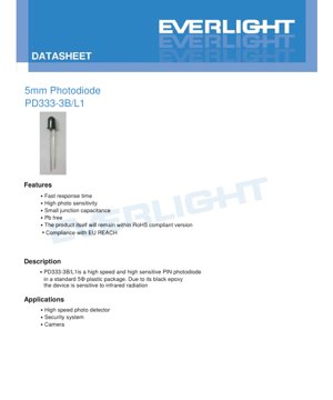
The PD333-3B/L1 is a high-speed, high-sensitivity silicon PIN photodiode encapsulated in a standard 5mm diameter plastic package. Its primary function is to convert incident light, particularly in the infrared spectrum, into an electrical current. The device features a black epoxy lens, which enhances its sensitivity to infrared radiation while minimizing response to visible light. This makes it particularly suitable for applications requiring detection in the near-infrared range. The core advantages of this component include its fast response time, high photosensitivity, and small junction capacitance, which are critical for high-speed signal detection. It is designed as a lead-free (Pb-free) component and complies with relevant environmental regulations such as RoHS and EU REACH.
2. Technical Parameter Deep Dive
2.1 Absolute Maximum Ratings
The device is designed to operate reliably within specified limits. Exceeding these ratings may cause permanent damage.
- Reverse Voltage (VR): 32 V - The maximum reverse bias voltage that can be applied across the photodiode terminals.
- Operating Temperature (Topr): -25°C to +85°C - The ambient temperature range for normal operation.
- Storage Temperature (Tstg): -40°C to +100°C - The temperature range for non-operational storage.
- Soldering Temperature (Tsol): 260°C - The peak temperature the device can withstand during soldering processes.
- Power Dissipation (Pc): 150 mW - The maximum power the device can dissipate at or below 25°C ambient temperature.
2.2 Electro-Optical Characteristics
These parameters define the photodiode's performance under standard test conditions (Ta=25°C).
- Spectral Bandwidth (λ0.5): 840 nm to 1100 nm - The wavelength range where the responsivity is at least half of its peak value.
- Peak Sensitivity Wavelength (λP): 940 nm (Typical) - The wavelength of light at which the photodiode is most sensitive.
- Open-Circuit Voltage (VOC): 0.44 V (Typical) - The voltage generated across the open terminals when illuminated (Ee=5 mW/cm², λp=940nm).
- Short-Circuit Current (ISC): 10 µA (Typical) - The current flowing when the terminals are short-circuited under illumination (Ee=1 mW/cm², λp=940nm).
- Reverse Light Current (IL): Min. 15 µA - The photocurrent generated under reverse bias (VR=5V, Ee=1 mW/cm², λp=940nm). This is a key parameter for signal detection.
- Reverse Dark Current (ID): Max. 30 nA - The small leakage current that flows under reverse bias in complete darkness (VR=10V). A lower value is desirable for better signal-to-noise ratio.
- Reverse Breakdown Voltage (VBR): Min. 32 V, Typ. 170 V - The reverse voltage at which the junction breaks down and current increases sharply.
- Total Capacitance (Ct): 6.0 pF (Typical) - The junction capacitance under reverse bias (VR=5V, f=1MHz). A low capacitance is crucial for high-speed operation.
- Rise/Fall Time (tr/tf): 10 ns (Typical) - The time required for the output signal to rise from 10% to 90% (or fall from 90% to 10%) of its final value (VR=10V, RL=100Ω). This defines the maximum switching speed.
3. Binning System Explanation
The PD333-3B/L1 is sorted into different bins based on its Reverse Light Current (IL) performance under specific test conditions (Ee=1mW/cm², λp=940nm, VR=5V). This allows designers to select components with consistent performance for their application.
| Bin Number | Min IL (µA) | Max IL (µA) |
|---|---|---|
| BIN1 | 15 | 25 |
| BIN2 | 25 | 35 |
| BIN3 | 35 | 45 |
| BIN4 | 45 | 55 |
| BIN5 | 55 | 65 |
The datasheet also notes standard tolerances: Luminous Intensity ±10%, Dominant Wavelength ±1nm, and Forward Voltage ±0.1V, though the latter two are more relevant to LEDs than this photodiode.
4. Performance Curve Analysis
The datasheet includes several characteristic curves that illustrate device behavior under varying conditions. These are essential for circuit design and performance prediction.
4.1 Spectral Sensitivity
The spectral response curve shows the device's relative sensitivity across different wavelengths. It peaks at 940 nm (infrared) and has significant response from approximately 840 nm to 1100 nm. This confirms its suitability for IR-based systems like remote controls and proximity sensors.
4.2 Temperature Dependence
Curves are provided showing the relationship between Reverse Dark Current and Ambient Temperature, and Power Dissipation vs. Ambient Temperature. The dark current typically increases with temperature, which can affect the noise floor in sensitive applications. The power derating curve shows how the maximum allowable power dissipation decreases as ambient temperature rises above 25°C.
4.3 Electrical Characteristics
Key graphs include:
- Reverse Light Current vs. Irradiance (Ee): Shows the linear relationship between generated photocurrent and incident light power density, a fundamental property of photodiodes.
- Terminal Capacitance vs. Reverse Voltage: Demonstrates how junction capacitance decreases with increasing reverse bias voltage. Operating at a higher reverse voltage (within limits) can improve speed by reducing capacitance.
- Response Time vs. Load Resistance: Illustrates how the rise/fall time is affected by the load resistor (RL) in the circuit. A smaller RL generally leads to faster response but a smaller output voltage swing.
5. Mechanical and Package Information
The device uses a standard 5mm diameter round plastic package. The package dimension drawing provides critical measurements for PCB footprint design and mechanical integration. Key dimensions include the overall diameter (5mm), lead spacing, and component height. The drawing specifies a general tolerance of ±0.25mm unless otherwise noted. The package features two axial leads for electrical connection. The black epoxy body acts as the lens and IR filter. Proper polarity identification should be based on the datasheet's terminal diagram; typically, the cathode is indicated by a longer lead, a flat spot on the package, or a specific marking.
6. Soldering and Assembly Guidelines
The component is rated for a maximum soldering temperature of 260°C. Standard reflow or wave soldering profiles for lead-free processes can be used, ensuring the peak temperature and time above liquidus are controlled to prevent thermal damage. Hand soldering should be performed quickly with a temperature-controlled iron. It is recommended to store the components in a dry environment to prevent moisture absorption, which could cause issues during soldering (popcorning).
7. Packaging and Ordering Information
The standard packing specification is 500 pieces per bag, 5 bags per box, and 10 boxes per carton, totaling 25,000 pieces per carton. The label on the packaging includes fields for Customer Product Number (CPN), Product Number (P/N), Packing Quantity (QTY), and relevant performance ranks (CAT for intensity, etc.), along with Lot Number and date coding for traceability.
8. Application Suggestions
8.1 Typical Application Scenarios
- High-Speed Photo Detection: Suitable for data transmission over fiber optics, barcode scanners, and optical encoders due to its 10ns response time.
- Security Systems: Can be used in intrusion detection beams, smoke detectors, or as a receiver for IR-based security communication.
- Camera Applications: Useful for light metering, auto-focus assist systems, or as an IR cut-filter monitor.
- Industrial Sensing: Object detection, counting, and position sensing in automated equipment.
8.2 Design Considerations
- Bias Circuit: The photodiode can be used in photovoltaic (zero bias) mode for low-noise applications or photoconductive (reverse bias) mode for higher speed and linearity. The 32V maximum reverse voltage allows for a wide range of bias choices.
- Amplification: The output current is small (microamps), so a transimpedance amplifier (TIA) is almost always required to convert the current to a usable voltage signal.
- Noise: For sensitive applications, consider the dark current and its temperature dependence. Shielding and careful PCB layout are necessary to minimize pickup of electrical noise.
- Optical Filtering: The black epoxy provides some filtering, but for specific wavelength selection, an additional bandpass optical filter may be needed.
9. Technical Comparison and Differentiation
Compared to generic photodiodes, the PD333-3B/L1 offers a balanced combination of speed (10ns), sensitivity (min 15µA @ specified conditions), and a robust 32V reverse voltage rating in a common 5mm package. Its silicon construction and PIN structure provide a good trade-off between cost, speed, and sensitivity for near-IR applications. Alternatives might include photodiodes with smaller packages for space-constrained designs, those with different spectral responses (e.g., visible light), or avalanche photodiodes (APDs) for applications requiring internal gain, though APDs are more complex and expensive.
10. Frequently Asked Questions (FAQ)
Q: What is the difference between photovoltaic and photoconductive mode?
A: In photovoltaic mode (zero bias), the photodiode generates its own voltage/current, offering very low dark current and noise. In photoconductive mode (reverse bias), an external voltage is applied, which reduces junction capacitance (increasing speed) and improves linearity, at the cost of slightly higher dark current.
Q: How do I choose the right bin?
A: Select a bin based on the required minimum signal current for your application. Using a higher bin ensures a stronger signal but may have cost implications. For consistency in production, specify a single bin.
Q: Can this photodiode be used for visible light detection?
A: While it has some response in the visible red spectrum, its peak is at 940nm (IR), and the black epoxy attenuates visible light. For primary visible light detection, a photodiode with a clear or color-specific lens and a peak wavelength in the visible range would be more appropriate.
Q: What value of load resistor (RL) should I use?
A: It depends on the required speed and signal level. A smaller RL (e.g., 50Ω) gives faster response but a smaller voltage output (Vout = Iph * RL). A larger RL gives a larger voltage but slower response due to the RC time constant formed with the diode capacitance. Refer to the "Response Time vs. Load Resistance" curve.
11. Practical Design Case
Case: Simple Object Detection Sensor
A common use is a break-beam sensor. An IR LED emitting at 940nm is placed opposite the PD333-3B/L1 photodiode. The photodiode is operated in photoconductive mode with a 5V reverse bias through a load resistor (e.g., 10kΩ). Under normal conditions, the IR light hits the diode, generating a photocurrent and creating a voltage drop across the resistor. When an object breaks the beam, the photocurrent drops significantly, causing a large change in the voltage across the resistor. This voltage signal can be fed into a comparator to generate a digital interrupt for a microcontroller. The 10ns response time is far faster than needed for this application, but the high sensitivity ensures reliable operation even with weaker IR sources or over longer distances.
12. Principle of Operation
A PIN photodiode is a semiconductor device with an intrinsic (I) region sandwiched between P-type and N-type regions. When photons with energy greater than the semiconductor's bandgap strike the device, they create electron-hole pairs in the intrinsic region. Under the influence of an internal built-in potential (photovoltaic mode) or an applied reverse bias (photoconductive mode), these charge carriers are swept apart, creating a measurable photocurrent that is proportional to the incident light intensity. The wide intrinsic region in a PIN structure reduces junction capacitance compared to a standard PN photodiode, enabling higher speed operation.
13. Industry Trends
The demand for photodiodes continues to grow in areas like consumer electronics (smartphone sensors, wearables), automotive (LiDAR, driver monitoring), industrial automation, and communication (data centers). Trends include further miniaturization into chip-scale packages, integration with on-chip amplification and signal processing circuitry, development of photodiodes for new wavelength ranges (e.g., short-wave infrared), and enhancement of performance parameters like lower noise and higher speed to meet the requirements of emerging technologies.
LED Specification Terminology
Complete explanation of LED technical terms
Photoelectric Performance
| Term | Unit/Representation | Simple Explanation | Why Important |
|---|---|---|---|
| Luminous Efficacy | lm/W (lumens per watt) | Light output per watt of electricity, higher means more energy efficient. | Directly determines energy efficiency grade and electricity cost. |
| Luminous Flux | lm (lumens) | Total light emitted by source, commonly called "brightness". | Determines if the light is bright enough. |
| Viewing Angle | ° (degrees), e.g., 120° | Angle where light intensity drops to half, determines beam width. | Affects illumination range and uniformity. |
| CCT (Color Temperature) | K (Kelvin), e.g., 2700K/6500K | Warmth/coolness of light, lower values yellowish/warm, higher whitish/cool. | Determines lighting atmosphere and suitable scenarios. |
| CRI / Ra | Unitless, 0–100 | Ability to render object colors accurately, Ra≥80 is good. | Affects color authenticity, used in high-demand places like malls, museums. |
| SDCM | MacAdam ellipse steps, e.g., "5-step" | Color consistency metric, smaller steps mean more consistent color. | Ensures uniform color across same batch of LEDs. |
| Dominant Wavelength | nm (nanometers), e.g., 620nm (red) | Wavelength corresponding to color of colored LEDs. | Determines hue of red, yellow, green monochrome LEDs. |
| Spectral Distribution | Wavelength vs intensity curve | Shows intensity distribution across wavelengths. | Affects color rendering and quality. |
Electrical Parameters
| Term | Symbol | Simple Explanation | Design Considerations |
|---|---|---|---|
| Forward Voltage | Vf | Minimum voltage to turn on LED, like "starting threshold". | Driver voltage must be ≥Vf, voltages add up for series LEDs. |
| Forward Current | If | Current value for normal LED operation. | Usually constant current drive, current determines brightness & lifespan. |
| Max Pulse Current | Ifp | Peak current tolerable for short periods, used for dimming or flashing. | Pulse width & duty cycle must be strictly controlled to avoid damage. |
| Reverse Voltage | Vr | Max reverse voltage LED can withstand, beyond may cause breakdown. | Circuit must prevent reverse connection or voltage spikes. |
| Thermal Resistance | Rth (°C/W) | Resistance to heat transfer from chip to solder, lower is better. | High thermal resistance requires stronger heat dissipation. |
| ESD Immunity | V (HBM), e.g., 1000V | Ability to withstand electrostatic discharge, higher means less vulnerable. | Anti-static measures needed in production, especially for sensitive LEDs. |
Thermal Management & Reliability
| Term | Key Metric | Simple Explanation | Impact |
|---|---|---|---|
| Junction Temperature | Tj (°C) | Actual operating temperature inside LED chip. | Every 10°C reduction may double lifespan; too high causes light decay, color shift. |
| Lumen Depreciation | L70 / L80 (hours) | Time for brightness to drop to 70% or 80% of initial. | Directly defines LED "service life". |
| Lumen Maintenance | % (e.g., 70%) | Percentage of brightness retained after time. | Indicates brightness retention over long-term use. |
| Color Shift | Δu′v′ or MacAdam ellipse | Degree of color change during use. | Affects color consistency in lighting scenes. |
| Thermal Aging | Material degradation | Deterioration due to long-term high temperature. | May cause brightness drop, color change, or open-circuit failure. |
Packaging & Materials
| Term | Common Types | Simple Explanation | Features & Applications |
|---|---|---|---|
| Package Type | EMC, PPA, Ceramic | Housing material protecting chip, providing optical/thermal interface. | EMC: good heat resistance, low cost; Ceramic: better heat dissipation, longer life. |
| Chip Structure | Front, Flip Chip | Chip electrode arrangement. | Flip chip: better heat dissipation, higher efficacy, for high-power. |
| Phosphor Coating | YAG, Silicate, Nitride | Covers blue chip, converts some to yellow/red, mixes to white. | Different phosphors affect efficacy, CCT, and CRI. |
| Lens/Optics | Flat, Microlens, TIR | Optical structure on surface controlling light distribution. | Determines viewing angle and light distribution curve. |
Quality Control & Binning
| Term | Binning Content | Simple Explanation | Purpose |
|---|---|---|---|
| Luminous Flux Bin | Code e.g., 2G, 2H | Grouped by brightness, each group has min/max lumen values. | Ensures uniform brightness in same batch. |
| Voltage Bin | Code e.g., 6W, 6X | Grouped by forward voltage range. | Facilitates driver matching, improves system efficiency. |
| Color Bin | 5-step MacAdam ellipse | Grouped by color coordinates, ensuring tight range. | Guarantees color consistency, avoids uneven color within fixture. |
| CCT Bin | 2700K, 3000K etc. | Grouped by CCT, each has corresponding coordinate range. | Meets different scene CCT requirements. |
Testing & Certification
| Term | Standard/Test | Simple Explanation | Significance |
|---|---|---|---|
| LM-80 | Lumen maintenance test | Long-term lighting at constant temperature, recording brightness decay. | Used to estimate LED life (with TM-21). |
| TM-21 | Life estimation standard | Estimates life under actual conditions based on LM-80 data. | Provides scientific life prediction. |
| IESNA | Illuminating Engineering Society | Covers optical, electrical, thermal test methods. | Industry-recognized test basis. |
| RoHS / REACH | Environmental certification | Ensures no harmful substances (lead, mercury). | Market access requirement internationally. |
| ENERGY STAR / DLC | Energy efficiency certification | Energy efficiency and performance certification for lighting. | Used in government procurement, subsidy programs, enhances competitiveness. |