Table of Contents
- 1. Product Overview
- 1.1 Core Advantages
- 1.2 Target Applications
- 2. Technical Parameter Analysis
- 2.1 Absolute Maximum Ratings
- 2.2 Electro-Optical Characteristics
- 3. Binning System Explanation The radiant intensity of this LED is categorized into different bins to ensure consistency in application design. The binning is defined at a forward current of 20mA. Bin M: Radiant Intensity range from 7.80 mW/sr to 12.50 mW/sr. Bin N: Radiant Intensity range from 11.0 mW/sr to 17.6 mW/sr. This allows designers to select LEDs with a guaranteed minimum output for their specific sensitivity requirements. 4. Performance Curve Analysis
- 4.1 Forward Current vs. Ambient Temperature
- 4.2 Radiant Intensity vs. Forward Current
- 4.3 Spectral Distribution
- 4.4 Relative Radiant Intensity vs. Angular Displacement
- 5. Mechanical and Package Information
- 5.1 Package Dimensions
- 5.2 Polarity Identification
- 6. Soldering and Assembly Guidelines
- 6.1 Lead Forming
- 6.2 Storage Conditions
- 6.3 Soldering Parameters
- 6.4 Cleaning
- 7. Thermal Management
- 8. Packaging and Ordering Information
- 8.1 Packing Specification
- 8.2 Label Information
- 9. Application Design Considerations
- 9.1 Driving the LED
- 9.2 Optical Design
- 9.3 Electrical Noise Immunity
- 10. Technical Comparison and Positioning
- 11. Frequently Asked Questions (FAQ)
- 11.1 What is the difference between Bin M and Bin N?
- 11.2 Can I drive this LED at 100mA continuously?
- 11.3 Why is the minimum soldering distance (3mm) important?
- 12. Design Use Case Example
- 13. Operating Principle
- 14. Technology Trends
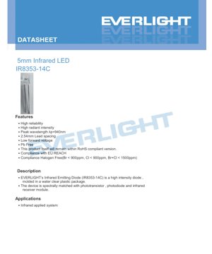
1. Product Overview
This document details the specifications for a high-intensity 5mm infrared (IR) emitting diode. The device is encapsulated in a water-clear plastic package, making it suitable for various infrared sensing and transmission applications. Its spectral output is specifically matched to work efficiently with common phototransistors, photodiodes, and infrared receiver modules.
1.1 Core Advantages
- High Reliability: Designed for consistent performance and long-term operation.
- High Radiant Intensity: Delivers strong infrared output for effective signal transmission.
- Low Forward Voltage: Typically 1.2V at 20mA, contributing to energy-efficient operation.
- Environmental Compliance: The product is compliant with RoHS, EU REACH, and is Halogen-Free (Br < 900ppm, Cl < 900ppm, Br+Cl < 1500ppm).
1.2 Target Applications
This IR LED is intended for use in various infrared systems, including but not limited to remote control units, proximity sensors, object detection, optical switches, and data transmission over short distances.
2. Technical Parameter Analysis
2.1 Absolute Maximum Ratings
The following ratings define the limits beyond which permanent damage to the device may occur. Operation under these conditions is not guaranteed.
- Continuous Forward Current (IF): 100 mA
- Peak Forward Current (IFP): 1.0 A (Pulse Width ≤100μs, Duty ≤1%)
- Reverse Voltage (VR): 5 V
- Operating Temperature (Topr): -40°C to +85°C
- Storage Temperature (Tstg): -40°C to +100°C
- Power Dissipation (Pd): 150 mW (at or below 25°C free air temperature)
2.2 Electro-Optical Characteristics
These parameters are measured at an ambient temperature (Ta) of 25°C and define the typical performance of the device.
- Radiant Intensity (Ie): 7.8 - 17.6 mW/sr (at IF=20mA, depending on bin). Up to 50 mW/sr typical at IF=100mA.
- Peak Wavelength (λp): 940 nm (at IF=20mA).
- Spectral Bandwidth (Δλ): 45 nm (at IF=20mA).
- Forward Voltage (VF): 1.2V (Typ.) / 1.5V (Max.) at 20mA; 1.4V (Typ.) / 1.8V (Max.) at 100mA.
- Reverse Current (IR): 10 μA (Max.) at VR=5V.
- View Angle (2θ1/2): 27° to 43° (at IF=20mA).
3. Binning System Explanation
The radiant intensity of this LED is categorized into different bins to ensure consistency in application design. The binning is defined at a forward current of 20mA.
- Bin M: Radiant Intensity range from 7.80 mW/sr to 12.50 mW/sr.
- Bin N: Radiant Intensity range from 11.0 mW/sr to 17.6 mW/sr.
This allows designers to select LEDs with a guaranteed minimum output for their specific sensitivity requirements.
4. Performance Curve Analysis
The datasheet includes several characteristic curves essential for circuit design and thermal management.
4.1 Forward Current vs. Ambient Temperature
This derating curve shows the maximum allowable continuous forward current as a function of the ambient temperature. As temperature increases, the maximum current must be reduced to prevent exceeding the device's power dissipation limits and to ensure long-term reliability. Designers must use this curve to select appropriate operating currents for their application's thermal environment.
4.2 Radiant Intensity vs. Forward Current
This graph illustrates the relationship between the drive current and the optical output power (radiant intensity). The output is generally linear over a range but will saturate at very high currents. It is crucial for determining the required drive current to achieve a desired signal strength at the receiver.
4.3 Spectral Distribution
The spectral curve confirms the peak emission at 940nm with a typical bandwidth of 45nm. This wavelength is ideal as it falls outside the visible spectrum, minimizing visible light interference, and is well-matched to the sensitivity of silicon-based photodetectors.
4.4 Relative Radiant Intensity vs. Angular Displacement
This polar plot defines the view angle (2θ1/2), which is the angle at which the radiant intensity drops to half of its value at 0° (on-axis). The specified range of 27° to 43° indicates the beam spread. A narrower angle provides more focused light, while a wider angle offers broader coverage.
5. Mechanical and Package Information
5.1 Package Dimensions
The device is housed in a standard 5mm round LED package. Key dimensions include the overall diameter (5.0mm typical), the lead spacing (2.54mm / 0.1 inches standard), and the distance from the base to the lens dome. The leads are typically 0.45mm in diameter. All dimensions have a tolerance of ±0.25mm unless otherwise specified. A detailed dimensioned drawing is provided in the original datasheet for precise PCB layout.
5.2 Polarity Identification
The cathode (negative lead) is typically identified by a flat spot on the plastic lens rim and/or by being the shorter lead. The anode (positive lead) is longer. Correct polarity must be observed during circuit assembly.
6. Soldering and Assembly Guidelines
6.1 Lead Forming
- Bends must be made at least 3mm from the base of the epoxy bulb.
- Forming must be done before soldering and at room temperature.
- Avoid stressing the package during bending or cutting.
- PCB holes must align perfectly with LED leads to avoid mounting stress.
6.2 Storage Conditions
- Recommended storage: ≤30°C and ≤70% Relative Humidity.
- Shelf life after shipment is 3 months under these conditions.
- For longer storage (up to 1 year), use a sealed container with nitrogen and desiccant.
- Avoid rapid temperature changes in humid environments to prevent condensation.
6.3 Soldering Parameters
Hand Soldering:
- Iron Tip Temperature: 300°C Max. (30W Max.)
- Soldering Time: 3 seconds Max. per lead.
- Minimum Distance from solder joint to epoxy bulb: 3mm.
Wave/DIP Soldering:
- Preheat Temperature: 100°C Max. (60 sec Max.)
- Solder Bath Temperature: 260°C Max.
- Bath Time: 5 seconds Max.
- Minimum Distance from solder joint to epoxy bulb: 3mm.
Critical Notes:
- Avoid stress on leads while the LED is hot.
- Do not solder (dip or hand) more than once.
- Protect the LED from shock/vibration until it cools to room temperature.
- Use the lowest possible soldering temperature that achieves a reliable joint.
6.4 Cleaning
- If necessary, clean only with isopropyl alcohol at room temperature for ≤1 minute.
- Do not use ultrasonic cleaning unless pre-qualified, as it can cause damage.
7. Thermal Management
Effective heat dissipation is critical for LED performance and lifetime. The current must be derated according to the "Forward Current vs. Ambient Temperature" curve. The temperature surrounding the LED in the final application must be controlled. This may involve using appropriate PCB copper area for heat sinking, ensuring adequate ventilation, or using heatsinks if high currents are driven continuously.
8. Packaging and Ordering Information
8.1 Packing Specification
- LEDs are packed in anti-static bags.
- Packing Quantity: 200-500 pieces per bag. 5 bags per inner carton. 10 inner cartons per master (outside) carton.
8.2 Label Information
The product label includes key identifiers: Customer Part Number (CPN), Product Number (P/N), Packing Quantity (QTY), Luminous Intensity Rank (CAT), Dominant Wavelength Rank (HUE), Forward Voltage Rank (REF), Lot Number, and a date code.
9. Application Design Considerations
9.1 Driving the LED
Always use a series current-limiting resistor. The resistor value can be calculated using Ohm's Law: R = (Vsupply - VF) / IF. Use the maximum VF from the datasheet for a conservative design. For pulsed operation (e.g., remote controls), ensure the peak current (IFP) and duty cycle limits are not exceeded to avoid overheating.
9.2 Optical Design
Consider the view angle when designing lenses or reflectors for the system. The 940nm wavelength is invisible, so an indicator LED or circuit feedback may be necessary for user confirmation of operation. Ensure the receiver (phototransistor, IC) is spectrally matched to 940nm for optimal sensitivity.
9.3 Electrical Noise Immunity
In electrically noisy environments, consider shielding the LED/receiver pair, using modulated IR signals (e.g., 38kHz carrier) with a corresponding demodulating receiver, and implementing software filtering to reject ambient light and noise spikes.
10. Technical Comparison and Positioning
This 5mm, 940nm IR LED offers a balance of performance and cost for general-purpose infrared applications. Its key differentiators are the relatively high radiant intensity (up to 17.6 mW/sr) from a standard 5mm package and the low forward voltage, which reduces power consumption. Compared to older 880nm or 850nm LEDs, the 940nm emission is less visible (no faint red glow), making it more suitable for discreet applications. For applications requiring extremely narrow beam angles or higher power, alternative package styles (e.g., side-view, high-power SMD) would be more appropriate.
11. Frequently Asked Questions (FAQ)
11.1 What is the difference between Bin M and Bin N?
Bin M and Bin N categorize the LED based on its minimum guaranteed radiant intensity at 20mA. Bin N LEDs have a higher minimum output (11.0 mW/sr) compared to Bin M (7.8 mW/sr). Choose Bin N for applications requiring stronger signal strength or longer range.
11.2 Can I drive this LED at 100mA continuously?
Yes, the absolute maximum rating for continuous forward current is 100mA. However, you must refer to the derating curve. At an ambient temperature of 25°C, 100mA is permissible, but as ambient temperature rises, the maximum allowable continuous current decreases to keep the junction temperature within safe limits. Adequate heat sinking is crucial for continuous high-current operation.
11.3 Why is the minimum soldering distance (3mm) important?
The 3mm distance prevents excessive heat from traveling up the lead and damaging the internal semiconductor die or the epoxy encapsulation during the soldering process. Excessive heat can cause cracking, delamination, or permanent electrical degradation.
12. Design Use Case Example
Scenario: Simple Object Proximity Sensor.
Design: Place the IR LED and a phototransistor side-by-side, facing the same direction. Drive the LED with a 20mA constant current (using a resistor from a 5V supply: R = (5V - 1.5V) / 0.02A = 175Ω, use 180Ω standard value). When an object comes within range, infrared light reflects off the object and into the phototransistor, causing its collector current to increase. This current change can be converted to a voltage via a pull-up resistor and fed into a comparator or microcontroller ADC to detect the object's presence. The 940nm wavelength helps reject visible ambient light. The choice between Bin M or N depends on the required sensing distance and object reflectivity.
13. Operating Principle
An Infrared Light Emitting Diode (IR LED) is a semiconductor p-n junction diode. When forward biased (positive voltage applied to the anode relative to the cathode), electrons and holes recombine in the active region, releasing energy in the form of photons. The specific semiconductor material used (Gallium Aluminum Arsenide - GaAlAs in this case) determines the wavelength of the emitted light. For GaAlAs, this results in infrared radiation centered around 940 nanometers, which is outside the visible spectrum. The water-clear lens does not filter or color the light, allowing maximum transmission of the infrared output.
14. Technology Trends
While discrete 5mm through-hole LEDs remain popular for prototyping, hobbyist projects, and some industrial applications, the industry trend is strongly towards surface-mount device (SMD) packages. SMD IR LEDs offer advantages like smaller footprint, better suitability for automated pick-and-place assembly, and often improved thermal performance due to direct mounting on the PCB. There is also ongoing development to increase the efficiency (more radiant output per electrical watt input) and reliability of IR emitters. However, the fundamental principle of operation and key parameters like wavelength, intensity, and view angle remain the critical selection criteria for any IR application.
LED Specification Terminology
Complete explanation of LED technical terms
Photoelectric Performance
| Term | Unit/Representation | Simple Explanation | Why Important |
|---|---|---|---|
| Luminous Efficacy | lm/W (lumens per watt) | Light output per watt of electricity, higher means more energy efficient. | Directly determines energy efficiency grade and electricity cost. |
| Luminous Flux | lm (lumens) | Total light emitted by source, commonly called "brightness". | Determines if the light is bright enough. |
| Viewing Angle | ° (degrees), e.g., 120° | Angle where light intensity drops to half, determines beam width. | Affects illumination range and uniformity. |
| CCT (Color Temperature) | K (Kelvin), e.g., 2700K/6500K | Warmth/coolness of light, lower values yellowish/warm, higher whitish/cool. | Determines lighting atmosphere and suitable scenarios. |
| CRI / Ra | Unitless, 0–100 | Ability to render object colors accurately, Ra≥80 is good. | Affects color authenticity, used in high-demand places like malls, museums. |
| SDCM | MacAdam ellipse steps, e.g., "5-step" | Color consistency metric, smaller steps mean more consistent color. | Ensures uniform color across same batch of LEDs. |
| Dominant Wavelength | nm (nanometers), e.g., 620nm (red) | Wavelength corresponding to color of colored LEDs. | Determines hue of red, yellow, green monochrome LEDs. |
| Spectral Distribution | Wavelength vs intensity curve | Shows intensity distribution across wavelengths. | Affects color rendering and quality. |
Electrical Parameters
| Term | Symbol | Simple Explanation | Design Considerations |
|---|---|---|---|
| Forward Voltage | Vf | Minimum voltage to turn on LED, like "starting threshold". | Driver voltage must be ≥Vf, voltages add up for series LEDs. |
| Forward Current | If | Current value for normal LED operation. | Usually constant current drive, current determines brightness & lifespan. |
| Max Pulse Current | Ifp | Peak current tolerable for short periods, used for dimming or flashing. | Pulse width & duty cycle must be strictly controlled to avoid damage. |
| Reverse Voltage | Vr | Max reverse voltage LED can withstand, beyond may cause breakdown. | Circuit must prevent reverse connection or voltage spikes. |
| Thermal Resistance | Rth (°C/W) | Resistance to heat transfer from chip to solder, lower is better. | High thermal resistance requires stronger heat dissipation. |
| ESD Immunity | V (HBM), e.g., 1000V | Ability to withstand electrostatic discharge, higher means less vulnerable. | Anti-static measures needed in production, especially for sensitive LEDs. |
Thermal Management & Reliability
| Term | Key Metric | Simple Explanation | Impact |
|---|---|---|---|
| Junction Temperature | Tj (°C) | Actual operating temperature inside LED chip. | Every 10°C reduction may double lifespan; too high causes light decay, color shift. |
| Lumen Depreciation | L70 / L80 (hours) | Time for brightness to drop to 70% or 80% of initial. | Directly defines LED "service life". |
| Lumen Maintenance | % (e.g., 70%) | Percentage of brightness retained after time. | Indicates brightness retention over long-term use. |
| Color Shift | Δu′v′ or MacAdam ellipse | Degree of color change during use. | Affects color consistency in lighting scenes. |
| Thermal Aging | Material degradation | Deterioration due to long-term high temperature. | May cause brightness drop, color change, or open-circuit failure. |
Packaging & Materials
| Term | Common Types | Simple Explanation | Features & Applications |
|---|---|---|---|
| Package Type | EMC, PPA, Ceramic | Housing material protecting chip, providing optical/thermal interface. | EMC: good heat resistance, low cost; Ceramic: better heat dissipation, longer life. |
| Chip Structure | Front, Flip Chip | Chip electrode arrangement. | Flip chip: better heat dissipation, higher efficacy, for high-power. |
| Phosphor Coating | YAG, Silicate, Nitride | Covers blue chip, converts some to yellow/red, mixes to white. | Different phosphors affect efficacy, CCT, and CRI. |
| Lens/Optics | Flat, Microlens, TIR | Optical structure on surface controlling light distribution. | Determines viewing angle and light distribution curve. |
Quality Control & Binning
| Term | Binning Content | Simple Explanation | Purpose |
|---|---|---|---|
| Luminous Flux Bin | Code e.g., 2G, 2H | Grouped by brightness, each group has min/max lumen values. | Ensures uniform brightness in same batch. |
| Voltage Bin | Code e.g., 6W, 6X | Grouped by forward voltage range. | Facilitates driver matching, improves system efficiency. |
| Color Bin | 5-step MacAdam ellipse | Grouped by color coordinates, ensuring tight range. | Guarantees color consistency, avoids uneven color within fixture. |
| CCT Bin | 2700K, 3000K etc. | Grouped by CCT, each has corresponding coordinate range. | Meets different scene CCT requirements. |
Testing & Certification
| Term | Standard/Test | Simple Explanation | Significance |
|---|---|---|---|
| LM-80 | Lumen maintenance test | Long-term lighting at constant temperature, recording brightness decay. | Used to estimate LED life (with TM-21). |
| TM-21 | Life estimation standard | Estimates life under actual conditions based on LM-80 data. | Provides scientific life prediction. |
| IESNA | Illuminating Engineering Society | Covers optical, electrical, thermal test methods. | Industry-recognized test basis. |
| RoHS / REACH | Environmental certification | Ensures no harmful substances (lead, mercury). | Market access requirement internationally. |
| ENERGY STAR / DLC | Energy efficiency certification | Energy efficiency and performance certification for lighting. | Used in government procurement, subsidy programs, enhances competitiveness. |