Table of Contents
- 1. Product Overview
- 2. In-Depth Technical Parameter Analysis
- 2.1 Absolute Maximum Ratings
- 2.2 Electro-Optical Characteristics
- 3. Binning System Explanation
- 4. Performance Curve Analysis
- 5. Mechanical and Package Information
- 5.1 Package Dimensions
- 5.2 Polarity Identification
- 6. Soldering and Assembly Guidelines
- 7. Packaging and Ordering Information
- 8. Application Recommendations
- 8.1 Typical Application Circuits
- 8.2 Design Considerations
- 9. Technical Comparison and Differentiation
- 10. Frequently Asked Questions (Based on Technical Parameters)
- 11. Practical Design and Usage Examples
- 12. Operating Principle
- 13. Technology Trends
- LED Specification Terminology
- Photoelectric Performance
- Electrical Parameters
- Thermal Management & Reliability
- Packaging & Materials
- Quality Control & Binning
- Testing & Certification
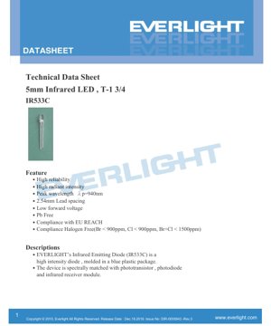
1. Product Overview
The IR533C is a high-intensity infrared emitting diode housed in a standard 5.0mm (T-1 3/4) blue plastic package. It is designed for applications requiring reliable and powerful infrared emission in the 940nm spectrum. The device is spectrally matched with common silicon phototransistors, photodiodes, and infrared receiver modules, making it an ideal source for closed-loop optical systems.
Key positioning of this component is in cost-effective, high-volume applications where consistent infrared output and standard package compatibility are paramount. Its core advantages include high reliability, significant radiant intensity output, and a low forward voltage characteristic, which contributes to efficient system power management.
The target market encompasses consumer electronics, industrial sensing, and safety equipment. It is particularly suited for designers of infrared remote control units, free-space optical data links, smoke detection systems, and various other infrared-based application systems.
2. In-Depth Technical Parameter Analysis
2.1 Absolute Maximum Ratings
These ratings define the stress limits beyond which permanent damage to the device may occur. Operation under or at these limits is not guaranteed.
- Continuous Forward Current (IF): 100 mA. This is the maximum DC current that can be passed through the LED indefinitely at an ambient temperature of 25°C.
- Peak Forward Current (IFP): 1.0 A. This high current is permissible only under pulsed conditions with a pulse width ≤100μs and a duty cycle ≤1%. This rating is crucial for applications requiring brief, high-intensity bursts of IR light.
- Reverse Voltage (VR): 5 V. Exceeding this reverse bias voltage can cause junction breakdown.
- Power Dissipation (Pd): 150 mW at or below 25°C free air temperature. This parameter, combined with thermal resistance, dictates the maximum allowable power under continuous operation.
- Temperature Ranges: The device is rated for operation from -40°C to +85°C and can be stored from -40°C to +100°C.
- Soldering Temperature (Tsol): 260°C for a duration not exceeding 5 seconds, compliant with typical lead-free reflow profiles.
2.2 Electro-Optical Characteristics
These parameters are measured at a standard ambient temperature of 25°C and define the device's performance under specified conditions.
- Radiant Intensity (Ie): This is the primary measure of optical output power per solid angle (steradian).
- At a standard drive current of 20mA DC, the typical radiant intensity is 7.8 mW/sr, with a minimum of 4.0 mW/sr.
- Under pulsed operation at 100mA (≤100μs, ≤1% duty), the output increases significantly.
- At the maximum pulsed current of 1A, the typical radiant intensity reaches 350 mW/sr, showcasing its capability for high-power, short-duration emission.
- Peak Wavelength (λp): 940 nm (typical). This wavelength is ideal as it falls within a high-transmission window for many plastics and glasses and is well-matched to the peak sensitivity of silicon detectors, while being largely invisible to the human eye.
- Spectral Bandwidth (Δλ): Approximately 45 nm (typical). This defines the spectral width of the emitted light at half its maximum intensity (FWHM).
- Forward Voltage (VF): A key parameter for circuit design.
- At 20mA, VF is typically 1.5V with a maximum of 1.5V.
- At 100mA pulsed, it rises to a typical 1.4V (max 1.85V).
- At 1A pulsed, the typical VF is 2.6V (max 4.0V), indicating increased junction voltage drop at very high currents.
- View Angle (2θ1/2): 25 degrees (typical). This is the full angle at which the radiant intensity drops to half of its value at 0 degrees (on-axis). A 25-degree angle provides a moderately focused beam.
- Reverse Current (IR): Maximum of 10 μA at VR=5V, indicating good junction quality.
3. Binning System Explanation
The datasheet includes a binning table for Radiant Intensity at IF=20mA. Binning is a quality control process where LEDs are sorted (binned) based on measured performance parameters after manufacture.
Radiant Intensity Binning: LEDs are categorized into bins (K, L, M, N, P) based on their measured radiant intensity. For example, bin 'K' includes LEDs with intensity between 4.0 and 6.4 mW/sr, while bin 'P' includes those between 15.0 and 24.0 mW/sr. This allows designers to select parts with guaranteed minimum (and maximum) output levels for their application, ensuring consistency in system performance, especially in multi-LED arrays or sensitive receiver systems. The specific bin for a given lot is indicated on the packaging label.
4. Performance Curve Analysis
The datasheet provides several characteristic curves that illustrate performance trends beyond the single-point data in the tables.
- Forward Current vs. Ambient Temperature (Fig.1): This curve shows how the maximum allowable continuous forward current derates as the ambient temperature increases above 25°C. To prevent overheating, the drive current must be reduced at higher temperatures.
- Spectral Distribution (Fig.2): A graph plotting relative intensity against wavelength, visually confirming the 940nm peak and the ~45nm bandwidth.
- Peak Emission Wavelength vs. Ambient Temperature (Fig.3): Illustrates the shift in peak wavelength (typically a slight increase) as the junction temperature changes. This is important for applications with tight spectral filtering.
- Forward Current vs. Forward Voltage (IV Curve) (Fig.4): Shows the non-linear relationship between current and voltage. The curve becomes steeper at higher currents due to series resistance in the semiconductor and package.
- Relative Intensity vs. Forward Current (Fig.5): Demonstrates the sub-linear relationship between drive current and light output. Efficiency (light output per unit current) often decreases at very high currents.
- Relative Radiant Intensity vs. Angular Displacement (Fig.6): This is the spatial radiation pattern, graphically defining the 25-degree view angle. It shows how intensity falls off as you move away from the central axis.
- Relative Intensity vs. Ambient Temperature (Fig.7): Shows the decrease in light output as the ambient (and thus junction) temperature rises, a phenomenon known as thermal quenching.
- Forward Voltage vs. Ambient Temperature (Fig.8): Indicates how the forward voltage drop decreases with increasing temperature, which is a characteristic of the semiconductor junction.
5. Mechanical and Package Information
5.1 Package Dimensions
The IR533C uses the industry-standard 5.0mm (T-1 3/4) radial leaded package. Key dimensional specifications from the drawing include:
- Overall diameter: 5.0mm (nominal).
- Lead spacing: 2.54mm (0.1 inches), compatible with standard perforated boards and sockets.
- Package body is molded in blue-tinted plastic, which is typical for infrared LEDs to indicate function and may offer some filtering.
- The lens is water clear.
- The chip material is Gallium Aluminum Arsenide (GaAlAs).
- All dimensional tolerances are ±0.25mm unless otherwise specified.
5.2 Polarity Identification
Like most radial LEDs, one lead is longer than the other. The longer lead is the anode (positive, A+), and the shorter lead is the cathode (negative, K-). The package may also have a flat spot on the rim near the cathode lead. Correct polarity is essential for operation.
6. Soldering and Assembly Guidelines
- Hand Soldering: Use a temperature-controlled iron. Limit soldering time per lead to a maximum of 3-5 seconds at a temperature not exceeding 350°C to prevent thermal damage to the plastic package and internal wire bonds.
- Wave Soldering: Is possible but requires careful control of preheat and solder wave temperature profiles to stay within the 260°C for 5 seconds maximum rating.
- Cleaning: If cleaning is necessary after soldering, use appropriate solvents that are compatible with the blue plastic package material. Avoid ultrasonic cleaning which can damage the internal die structure.
- Bending Leads: If lead forming is required, bend the leads at a point no closer than 3mm from the package body to avoid stress on the seal. Use proper tools to avoid nicking or damaging the leads.
- Storage Conditions: Store in a dry, anti-static environment at temperatures between -40°C and +100°C. Moisture Sensitivity Level (MSL) is not explicitly stated but treating it as MSL 2A or better (floor life >1 year) is typical for this package type.
7. Packaging and Ordering Information
- Packaging Specification: The LEDs are typically packed in bags containing 200 to 500 pieces. Five bags are placed in one box, and ten boxes constitute one shipping carton.
- Label Information: The packaging label includes critical information for traceability and identification:
- CPN (Customer's Part Number): As assigned by the purchaser.
- P/N (Production Number): The manufacturer's part number (IR533C).
- QTY (Packing Quantity): Number of pieces in the bag/box.
- CAT (Ranks): The performance bin code (e.g., M for radiant intensity).
- HUE: The peak wavelength bin.
- LOT No: The unique manufacturing lot number for traceability.
8. Application Recommendations
8.1 Typical Application Circuits
Basic Drive Circuit: The simplest circuit involves a series current-limiting resistor connected to a voltage supply. The resistor value (R) is calculated using Ohm's Law: R = (Vcc - VF) / IF, where Vcc is the supply voltage, VF is the LED forward voltage at the desired current IF, and IF is the target forward current (e.g., 20mA). Always ensure the power rating of the resistor is adequate (P = IF² * R).
Pulsed Operation for High Intensity: For applications like long-range remote controls, use the pulsed ratings. A transistor (BJT or MOSFET) can be used to switch the high pulsed current (up to 1A) from a capacitor or a higher voltage supply. The series resistor must be calculated based on the pulsed VF and the desired pulse current. Ensure the pulse width and duty cycle constraints (≤100μs, ≤1%) are strictly adhered to.
8.2 Design Considerations
- Heat Sinking: While the package has limited thermal dissipation capability, for continuous operation near the maximum current (100mA), consider the ambient temperature and provide adequate ventilation. The derating curve (Fig.1) must be followed.
- Optical Design: The 25-degree view angle provides natural focusing. For narrower beams, external lenses or reflectors can be used. For wider coverage, multiple LEDs or diffusers may be necessary.
- Receiver Matching: Ensure the receiver (phototransistor, photodiode, or IC) is sensitive in the 940nm region. Using a matching IR filter on the receiver can greatly improve signal-to-noise ratio by blocking ambient visible light.
- Electrical Noise: In sensitive analog sensing applications, drive the LED with a constant current source rather than a simple resistor for more stable output. For digital pulsed systems, ensure fast rise/fall times of the drive signal.
9. Technical Comparison and Differentiation
The IR533C positions itself within the broad 5mm IR LED market through specific characteristics:
- High Radiant Intensity: Its typical 7.8 mW/sr at 20mA and capability for very high pulsed output (350 mW/sr at 1A) make it suitable for applications requiring longer range or higher signal strength compared to standard low-power IR LEDs.
- 940nm Wavelength: This is the most common and versatile IR wavelength. It offers a good balance between silicon detector sensitivity, availability of matching filters, and relative eye safety compared to shorter near-IR wavelengths.
- Standard Package: The ubiquitous 5mm form factor ensures easy integration into existing designs, prototyping boards, and standard panel cutouts.
- Low Forward Voltage: A typical VF of 1.5V at 20mA allows efficient operation from low-voltage logic supplies (3.3V, 5V) with minimal voltage drop across the current-limiting resistor, leaving more headroom for stable operation.
- Compliance: Stated compliance with RoHS (Pb-Free), EU REACH, and Halogen-Free standards addresses modern environmental and regulatory requirements for electronic components.
10. Frequently Asked Questions (Based on Technical Parameters)
Q1: Can I drive this LED continuously at 100mA?
A1: The Absolute Maximum Rating for continuous forward current is 100mA at Ta=25°C. However, you must consult the derating curve (Fig.1). At elevated ambient temperatures, the maximum allowable continuous current decreases significantly to prevent exceeding the maximum junction temperature and the 150mW power dissipation limit. For reliable long-term operation, designing for a lower current (e.g., 50-75mA) is often advisable.
Q2: What is the difference between Radiant Intensity (mW/sr) and Radiant Power (mW)?
A2: Radiant Intensity is the optical power emitted per unit solid angle (steradian). Radiant Power (or Flux) is the total optical power emitted in all directions. To estimate total power, you would need to integrate the intensity over the entire spatial emission pattern (Fig.6). For a 25-degree view angle LED, the total power is significantly less than the on-axis intensity value multiplied by 4π steradians.
Q3: How do I select the correct current-limiting resistor?
A3: Use the formula R = (Vs - VF) / IF. Use the *maximum* VF from the datasheet for your chosen IF to ensure enough voltage drop across the resistor under all conditions, preventing overcurrent. For example, for a 5V supply and 20mA target: R = (5V - 1.5V) / 0.02A = 175 Ohms. Use the next standard value (180 Ohms). Power in the resistor: P = (0.02A)² * 180Ω = 0.072W, so a 1/8W or 1/4W resistor is safe.
Q4: Why is the forward voltage lower at 100mA pulsed than at 20mA DC in the table?
A4: This appears to be a discrepancy in the provided data (Typ. 1.4V at 100mA pulsed vs. 1.5V at 20mA). In reality, VF should increase with current due to series resistance. The pulsed measurement at 100mA might have a lower junction temperature rise than a DC measurement at 20mA, which could slightly affect VF. Always design using the *maximum* specified VF for your operating condition to be safe.
11. Practical Design and Usage Examples
Example 1: Long-Range Infrared Remote Control Transmitter.
Objective: Achieve a range of 30 meters in indoor conditions.
Design: Use pulsed operation at the maximum rating. Drive the IR533C with 1A pulses of 50μs width at a 1/40 duty cycle (e.g., 50μs on, 1950μs off, meeting the ≤100μs, ≤1% spec). A simple circuit uses a microcontroller GPIO pin to drive the base of an NPN transistor (e.g., 2N2222) via a small base resistor. The collector of the transistor is connected to the LED anode, and the LED cathode is connected to ground through a low-value current-setting resistor calculated for 1A. The LED anode is also connected to a charged capacitor (e.g., 100μF) close to the LED to supply the high peak current. This setup leverages the high pulsed radiant intensity (350 mW/sr typ.) for maximum range.
Example 2: Proximity or Object Detection Sensor.
Objective: Detect an object within 10cm.
Design: Use continuous operation at a moderate current (e.g., 50mA) for stable output. Pair the IR533C with a matching silicon phototransistor placed a few centimeters away. Modulate the LED drive current at a specific frequency (e.g., 38kHz) using the microcontroller. The receiver circuit includes a bandpass filter tuned to 38kHz. This technique makes the system immune to ambient light changes (sunlight, room lights). The 940nm wavelength minimizes visible light interference. The low VF allows the system to run from a 3.3V microcontroller supply.
12. Operating Principle
An Infrared Light Emitting Diode (IR LED) is a semiconductor p-n junction diode. When forward biased (positive voltage applied to the p-side relative to the n-side), electrons from the n-region are injected across the junction into the p-region, and holes from the p-region are injected into the n-region. These injected minority carriers (electrons in p-region, holes in n-region) recombine with the majority carriers. In a direct bandgap semiconductor like Gallium Aluminum Arsenide (GaAlAs), a significant portion of this recombination event releases energy in the form of photons (light). The wavelength (color) of the emitted light is determined by the bandgap energy (Eg) of the semiconductor material, according to the equation λ ≈ 1240 / Eg (with Eg in electron-volts and λ in nanometers). For GaAlAs tuned for 940nm emission, the bandgap is approximately 1.32 eV. The specific doping and layer structure of the chip are engineered to maximize the efficiency of this radiative recombination process within the infrared spectrum.
13. Technology Trends
The fundamental technology behind devices like the IR533C is mature. However, trends in the broader IR LED market influence their application and development context:
- Increased Power and Efficiency: Ongoing material science research aims to improve the wall-plug efficiency (optical power out / electrical power in) of IR LEDs, allowing for brighter output or lower power consumption. This is driven by applications in time-of-flight (ToF) sensors, LiDAR, and facial recognition.
- Miniaturization: While 5mm remains popular for through-hole designs, surface-mount device (SMD) packages (e.g., 0805, 1206, and chip-scale packages) are becoming dominant for automated assembly and space-constrained designs like smartphones and wearables.
- Integrated Solutions: There is a trend towards combining the IR LED with a driver IC, photodetector, and sometimes even a microcontroller in a single module. These "sensor fusion" modules simplify design for end-users in applications like gesture control or presence detection.
- Wavelength Diversification: While 940nm is standard, other wavelengths like 850nm (often visible as a faint red glow) are used where some visibility is acceptable and silicon detector sensitivity is slightly higher. Longer wavelengths (1050nm, 1300nm, 1550nm) are used for specialized applications like eye-safe LiDAR and optical communications.
- Application Expansion: The growth of the Internet of Things (IoT), smart home automation, automotive driver monitoring, and biometric security is continuously creating new applications for reliable, low-cost infrared emitters like the IR533C.
LED Specification Terminology
Complete explanation of LED technical terms
Photoelectric Performance
| Term | Unit/Representation | Simple Explanation | Why Important |
|---|---|---|---|
| Luminous Efficacy | lm/W (lumens per watt) | Light output per watt of electricity, higher means more energy efficient. | Directly determines energy efficiency grade and electricity cost. |
| Luminous Flux | lm (lumens) | Total light emitted by source, commonly called "brightness". | Determines if the light is bright enough. |
| Viewing Angle | ° (degrees), e.g., 120° | Angle where light intensity drops to half, determines beam width. | Affects illumination range and uniformity. |
| CCT (Color Temperature) | K (Kelvin), e.g., 2700K/6500K | Warmth/coolness of light, lower values yellowish/warm, higher whitish/cool. | Determines lighting atmosphere and suitable scenarios. |
| CRI / Ra | Unitless, 0–100 | Ability to render object colors accurately, Ra≥80 is good. | Affects color authenticity, used in high-demand places like malls, museums. |
| SDCM | MacAdam ellipse steps, e.g., "5-step" | Color consistency metric, smaller steps mean more consistent color. | Ensures uniform color across same batch of LEDs. |
| Dominant Wavelength | nm (nanometers), e.g., 620nm (red) | Wavelength corresponding to color of colored LEDs. | Determines hue of red, yellow, green monochrome LEDs. |
| Spectral Distribution | Wavelength vs intensity curve | Shows intensity distribution across wavelengths. | Affects color rendering and quality. |
Electrical Parameters
| Term | Symbol | Simple Explanation | Design Considerations |
|---|---|---|---|
| Forward Voltage | Vf | Minimum voltage to turn on LED, like "starting threshold". | Driver voltage must be ≥Vf, voltages add up for series LEDs. |
| Forward Current | If | Current value for normal LED operation. | Usually constant current drive, current determines brightness & lifespan. |
| Max Pulse Current | Ifp | Peak current tolerable for short periods, used for dimming or flashing. | Pulse width & duty cycle must be strictly controlled to avoid damage. |
| Reverse Voltage | Vr | Max reverse voltage LED can withstand, beyond may cause breakdown. | Circuit must prevent reverse connection or voltage spikes. |
| Thermal Resistance | Rth (°C/W) | Resistance to heat transfer from chip to solder, lower is better. | High thermal resistance requires stronger heat dissipation. |
| ESD Immunity | V (HBM), e.g., 1000V | Ability to withstand electrostatic discharge, higher means less vulnerable. | Anti-static measures needed in production, especially for sensitive LEDs. |
Thermal Management & Reliability
| Term | Key Metric | Simple Explanation | Impact |
|---|---|---|---|
| Junction Temperature | Tj (°C) | Actual operating temperature inside LED chip. | Every 10°C reduction may double lifespan; too high causes light decay, color shift. |
| Lumen Depreciation | L70 / L80 (hours) | Time for brightness to drop to 70% or 80% of initial. | Directly defines LED "service life". |
| Lumen Maintenance | % (e.g., 70%) | Percentage of brightness retained after time. | Indicates brightness retention over long-term use. |
| Color Shift | Δu′v′ or MacAdam ellipse | Degree of color change during use. | Affects color consistency in lighting scenes. |
| Thermal Aging | Material degradation | Deterioration due to long-term high temperature. | May cause brightness drop, color change, or open-circuit failure. |
Packaging & Materials
| Term | Common Types | Simple Explanation | Features & Applications |
|---|---|---|---|
| Package Type | EMC, PPA, Ceramic | Housing material protecting chip, providing optical/thermal interface. | EMC: good heat resistance, low cost; Ceramic: better heat dissipation, longer life. |
| Chip Structure | Front, Flip Chip | Chip electrode arrangement. | Flip chip: better heat dissipation, higher efficacy, for high-power. |
| Phosphor Coating | YAG, Silicate, Nitride | Covers blue chip, converts some to yellow/red, mixes to white. | Different phosphors affect efficacy, CCT, and CRI. |
| Lens/Optics | Flat, Microlens, TIR | Optical structure on surface controlling light distribution. | Determines viewing angle and light distribution curve. |
Quality Control & Binning
| Term | Binning Content | Simple Explanation | Purpose |
|---|---|---|---|
| Luminous Flux Bin | Code e.g., 2G, 2H | Grouped by brightness, each group has min/max lumen values. | Ensures uniform brightness in same batch. |
| Voltage Bin | Code e.g., 6W, 6X | Grouped by forward voltage range. | Facilitates driver matching, improves system efficiency. |
| Color Bin | 5-step MacAdam ellipse | Grouped by color coordinates, ensuring tight range. | Guarantees color consistency, avoids uneven color within fixture. |
| CCT Bin | 2700K, 3000K etc. | Grouped by CCT, each has corresponding coordinate range. | Meets different scene CCT requirements. |
Testing & Certification
| Term | Standard/Test | Simple Explanation | Significance |
|---|---|---|---|
| LM-80 | Lumen maintenance test | Long-term lighting at constant temperature, recording brightness decay. | Used to estimate LED life (with TM-21). |
| TM-21 | Life estimation standard | Estimates life under actual conditions based on LM-80 data. | Provides scientific life prediction. |
| IESNA | Illuminating Engineering Society | Covers optical, electrical, thermal test methods. | Industry-recognized test basis. |
| RoHS / REACH | Environmental certification | Ensures no harmful substances (lead, mercury). | Market access requirement internationally. |
| ENERGY STAR / DLC | Energy efficiency certification | Energy efficiency and performance certification for lighting. | Used in government procurement, subsidy programs, enhances competitiveness. |