Table of Contents
- 1. Product Overview
- 1.1 Core Features and Advantages
- 2. Technical Parameter Analysis
- 2.1 Absolute Maximum Ratings
- 2.2 Electro-Optical Characteristics
- 3. Binning System Explanation
- 4. Performance Curve Analysis
- 4.1 Forward Current vs. Ambient Temperature
- 4.2 Radiant Intensity vs. Forward Current
- 4.3 Spectral Distribution
- 4.4 Relative Radiant Intensity vs. Angular Displacement
- 5. Mechanical and Package Information
- 5.1 Package Dimensions
- 6. Soldering and Assembly Guidelines
- 6.1 Lead Forming
- 6.2 Storage
- 6.3 Soldering Process
- 6.4 Cleaning
- 7. Packaging and Ordering Information
- 7.1 Label Specification
- 7.2 Packing Specification
- 8. Application Suggestions and Design Considerations
- 8.1 Typical Application Scenarios
- 8.2 Design Considerations
- 9. Technical Comparison and Differentiation
- 10. Frequently Asked Questions (Based on Technical Parameters)
- 10.1 What is the difference between "radiant intensity" and "luminous intensity"?
- 10.2 Can I drive this LED at 100mA continuously?
- 10.3 Why is the peak forward current (1A) so much higher than the continuous current (100mA)?
- 10.4 How do I identify the anode and cathode?
- 11. Practical Design and Usage Examples
- 11.1 Simple Proximity Sensor Circuit
- 11.2 Driving an IR Receiver Module
- 12. Operating Principle
- 13. Technology Trends
- LED Specification Terminology
- Photoelectric Performance
- Electrical Parameters
- Thermal Management & Reliability
- Packaging & Materials
- Quality Control & Binning
- Testing & Certification
1. Product Overview
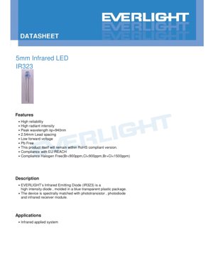
This document provides the complete technical specifications for a high-intensity 5mm infrared light-emitting diode (LED). The device is encapsulated in a blue transparent plastic package and is designed to emit light at a peak wavelength of 940 nanometers (nm), placing it firmly within the near-infrared spectrum. This wavelength is strategically chosen for optimal performance in sensing and remote control applications, as it is well-matched with the spectral sensitivity of common silicon phototransistors, photodiodes, and infrared receiver modules. The primary design goals for this component are high reliability, high radiant output, and low forward voltage operation, making it suitable for a variety of infrared-based electronic systems.
1.1 Core Features and Advantages
The LED offers several key advantages that contribute to its performance and ease of integration:
- High Radiant Intensity: Delivers a typical radiant intensity of 6.4 mW/sr at a standard drive current of 20mA, ensuring strong signal transmission.
- Low Forward Voltage: Features a typical forward voltage (Vf) of 1.2V at 20mA, contributing to lower power consumption in the overall system.
- Standardized Package: Utilizes a common 5mm radial leaded package with a 2.54mm (0.1 inch) lead spacing, compatible with standard PCB layouts and breadboards.
- Environmental Compliance: The product is manufactured to be Pb-Free, compliant with the EU RoHS and REACH regulations, and meets halogen-free standards (Br<900ppm, Cl<900ppm, Br+Cl<1500ppm).
- Defined Viewing Angle: Offers a typical half-intensity viewing angle (2θ1/2) of 30 degrees, providing a focused beam suitable for directed applications.
2. Technical Parameter Analysis
This section provides a detailed, objective interpretation of the device's electrical, optical, and thermal limits and characteristics.
2.1 Absolute Maximum Ratings
These ratings define the stress limits beyond which permanent damage to the device may occur. Operation under or at these limits is not guaranteed.
- Continuous Forward Current (IF): 100 mA. The maximum DC current that can be passed through the LED indefinitely at 25°C ambient temperature.
- Peak Forward Current (IFP): 1.0 A. This high pulse current is permissible only under strict conditions: pulse width ≤ 100μs and duty cycle ≤ 1%. This is useful for brief, high-intensity signaling.
- Reverse Voltage (VR): 5 V. The maximum voltage that can be applied in the reverse-biased direction. Exceeding this can cause junction breakdown.
- Power Dissipation (Pd): 150 mW at or below 25°C free air temperature. This is the maximum power the package can dissipate as heat. The rating derates with increasing ambient temperature.
- Temperature Ranges: Operating (Topr): -40°C to +85°C; Storage (Tstg): -40°C to +100°C.
- Soldering Temperature (Tsol): 260°C maximum for a duration not exceeding 5 seconds, defining the process window for wave or hand soldering.
2.2 Electro-Optical Characteristics
These parameters, measured at Ta=25°C, define the typical performance of the device under normal operating conditions.
- Radiant Intensity (Ie): The primary measure of optical output. Minimum 4.0 mW/sr, Typical 6.4 mW/sr at IF=20mA. At the maximum continuous current of 100mA, the typical intensity rises to 30 mW/sr.
- Peak Wavelength (λp): 940 nm (typical). This is the wavelength at which the emitted optical power is at its maximum.
- Spectral Bandwidth (Δλ): 45 nm (typical). This defines the range of wavelengths emitted, typically measured at half the peak power (Full Width at Half Maximum - FWHM).
- Forward Voltage (VF): 1.2V (typical), 1.5V (maximum) at 20mA. Increases to 1.4V (typical), 1.8V (maximum) at 100mA due to the diode's series resistance.
- Reverse Current (IR): Maximum 10 μA when a reverse bias of 5V is applied.
- View Angle (2θ1/2): 30 degrees (typical). The angular spread between the points where the radiant intensity is half of the value at 0 degrees (on-axis).
3. Binning System Explanation
The devices are sorted (binned) based on their measured radiant intensity at the standard test condition of IF = 20mA. This allows designers to select parts with guaranteed minimum and maximum output levels for consistent system performance.
| Bin Number | K | L | M | N | P |
|---|---|---|---|---|---|
| Min (mW/sr) | 4.0 | 5.6 | 7.8 | 11.0 | 15.0 |
| Max (mW/sr) | 6.4 | 8.9 | 12.5 | 17.6 | 24.0 |
For example, a part marked with Bin "L" is guaranteed to have a radiant intensity between 5.6 and 8.9 mW/sr. Higher bin letters (e.g., P) correspond to higher output devices. The datasheet does not indicate binning for other parameters like forward voltage or peak wavelength for this specific product, suggesting tight manufacturing control on those characteristics.
4. Performance Curve Analysis
The provided characteristic curves offer valuable insights into the device's behavior under varying conditions.
4.1 Forward Current vs. Ambient Temperature
This graph shows the derating of the maximum allowable continuous forward current as the ambient temperature increases. At 25°C, the full 100mA is permitted. As temperature rises, the maximum current must be reduced to prevent exceeding the 150mW power dissipation limit and to ensure long-term reliability. This curve is critical for designing systems that operate in elevated temperature environments.
4.2 Radiant Intensity vs. Forward Current
This plot illustrates the relationship between drive current (IF) and optical output (Ie). The radiant intensity increases super-linearly with current at lower levels and tends to become more linear at higher currents, though it will eventually saturate. The curve confirms the typical values stated in the table (e.g., ~6.4 mW/sr at 20mA, ~30 mW/sr at 100mA).
4.3 Spectral Distribution
The spectral graph plots relative radiant intensity against wavelength. It visually confirms the peak wavelength (λp) of 940nm and the spectral bandwidth (Δλ) of approximately 45nm at the FWHM points. The curve is characteristic of a GaAlAs (Gallium Aluminum Arsenide) semiconductor material system.
4.4 Relative Radiant Intensity vs. Angular Displacement
This polar plot depicts the radiation pattern of the LED. It shows how the intensity decreases as the angle from the central axis (0°) increases. The angle where the intensity drops to 50% of its on-axis value defines the half-intensity viewing angle, shown here as approximately 30 degrees, resulting in a moderately focused beam.
5. Mechanical and Package Information
5.1 Package Dimensions
The device uses a standard 5mm radial leaded package. The dimensional drawing specifies the key measurements: overall diameter (5.0mm typical), lead wire diameter, the distance from the base of the lens to the bend in the leads, and the lead spacing (2.54mm). The drawing includes a note that tolerances are ±0.25mm unless otherwise specified. The longer lead typically indicates the anode (positive) connection.
6. Soldering and Assembly Guidelines
Proper handling is essential to maintain device integrity and performance.
6.1 Lead Forming
- Bending must occur at a point at least 3mm from the base of the epoxy lens to avoid stress on the seal.
- Forming should be completed before any soldering operation.
- Cutting leads should be done at room temperature to prevent thermal shock.
- PCB holes must align precisely with LED leads to avoid mounting stress.
6.2 Storage
- Recommended storage conditions are ≤30°C and ≤70% Relative Humidity (RH) for up to 3 months from shipment.
- For longer storage (up to one year), use a sealed container with a nitrogen atmosphere and desiccant.
- Avoid rapid temperature changes in humid environments to prevent condensation.
6.3 Soldering Process
Critical Rule: Maintain a minimum distance of 3mm from the solder joint to the epoxy bulb.
- Hand Soldering: Iron tip temperature ≤300°C (for a 30W max iron), soldering time ≤3 seconds per lead.
- Wave/Dip Soldering: Preheat ≤100°C for ≤60 seconds. Solder bath temperature ≤260°C for ≤5 seconds immersion time.
- Avoid stress on leads during high-temperature phases.
- Dip or hand soldering should not be performed more than once.
- Allow the LED to cool to room temperature gradually after soldering; avoid rapid quenching.
6.4 Cleaning
- If necessary, clean only with isopropyl alcohol at room temperature for no more than one minute.
- Do not use ultrasonic cleaning unless absolutely necessary and only after thorough pre-qualification testing, as it can cause mechanical damage.
7. Packaging and Ordering Information
7.1 Label Specification
The label on the packaging contains several codes: Customer's Product Number (CPN), Manufacturer's Product Number (P/N), Packing Quantity (QTY), and performance ranks for Luminous Intensity (CAT), Dominant Wavelength (HUE), and Forward Voltage (REF). It also includes the Lot Number and a date code (Month).
7.2 Packing Specification
- LEDs are packed in anti-static bags.
- Typical packing: 200-500 pieces per bag, 5 bags per inner carton, 10 inner cartons per master (outside) carton.
8. Application Suggestions and Design Considerations
8.1 Typical Application Scenarios
- Infrared Remote Controls: For TVs, audio systems, and other consumer electronics. The 940nm wavelength is ideal as it is invisible to the human eye but efficiently detected by silicon receivers.
- Proximity and Object Detection Sensors: Used in automatic faucets, hand dryers, security systems, and industrial counting equipment. An IR LED paired with a photodetector can sense the interruption or reflection of its beam.
- Optical Switches and Encoders: For detecting motion or position in printers, motor controls, and rotary encoders.
- Night Vision Illumination: Providing covert illumination for security cameras equipped with IR-sensitive sensors.
- Data Transmission: In short-range, line-of-sight optical data links (e.g., IrDA legacy systems).
8.2 Design Considerations
- Current Limiting: Always use a series current-limiting resistor when driving the LED from a voltage source. Calculate the resistor value using R = (Vsupply - VF) / IF. Do not connect directly to a voltage source.
- Heat Management: When operating near maximum current or in high ambient temperatures, consider the derating curve. Ensure adequate ventilation or heatsinking if necessary, especially for densely packed arrays.
- Optical Design: The 30-degree viewing angle provides a focused beam. For wider coverage, use multiple LEDs or secondary optics like diffusers. For longer range, lenses can be used to collimate the beam further.
- Electrical Noise Immunity: In sensing applications, modulate the IR signal (e.g., with a 38kHz carrier) to distinguish it from ambient infrared light (sunlight, incandescent bulbs). This greatly improves signal-to-noise ratio.
- Receiver Matching: Ensure the selected photodetector or receiver module (e.g., a 38kHz integrated receiver) is spectrally sensitive around 940nm for optimal performance.
9. Technical Comparison and Differentiation
While many 5mm IR LEDs exist, this device's combination of parameters offers specific advantages:
- vs. Higher Wavelength IR LEDs (e.g., 850nm): The 940nm emission is less visible as a faint red glow, making it more suitable for covert applications. However, silicon photodetectors are slightly less sensitive at 940nm than at 850nm, which is offset by this LED's high radiant intensity.
- vs. Standard Brightness IR LEDs: The availability of higher output bins (e.g., Bin N, P) allows for designs requiring longer range or lower drive currents for the same signal strength, improving power efficiency.
- vs. Surface-Mount IR LEDs: The through-hole package is easier for prototyping, hobbyist use, and applications where mechanical robustness of the connection is prioritized over board space.
- Key Differentiators: The clearly defined and relatively tight binning structure for intensity, combined with comprehensive environmental compliance (RoHS, REACH, Halogen-Free), makes this part suitable for modern, regulated electronic products.
10. Frequently Asked Questions (Based on Technical Parameters)
10.1 What is the difference between "radiant intensity" and "luminous intensity"?
Radiant intensity (measured in mW/sr) is the optical power emitted per solid angle, relevant for all wavelengths. Luminous intensity (measured in candela, mcd) weights the optical power by the sensitivity of the human eye (photopic curve). Since the human eye is nearly insensitive to 940nm infrared light, luminous intensity is essentially zero for this LED. Radiant intensity is the correct metric for IR components used with electronic sensors.
10.2 Can I drive this LED at 100mA continuously?
Yes, but only if the ambient temperature (Ta) is at or below 25°C, as per the Absolute Maximum Ratings. If the ambient temperature is higher, you must refer to the "Forward Current vs. Ambient Temperature" derating curve to find the new maximum allowable continuous current. For example, at 85°C, the maximum continuous current will be significantly lower than 100mA.
10.3 Why is the peak forward current (1A) so much higher than the continuous current (100mA)?
The 1A rating is for very short pulses (≤100μs) with a low duty cycle (≤1%). During such a brief pulse, the semiconductor junction does not have time to heat up significantly. The 100mA continuous rating is limited by the steady-state thermal dissipation capability of the package. The high pulse current enables applications like long-range, brief-burst signaling.
10.4 How do I identify the anode and cathode?
In a standard radial LED package, the longer lead is typically the anode (positive). Additionally, viewing the LED from the bottom, the lead on the side with a flat spot on the plastic lens rim is usually the cathode (negative). Always verify with a multimeter in diode test mode if unsure.
11. Practical Design and Usage Examples
11.1 Simple Proximity Sensor Circuit
A basic reflective sensor can be built by placing this IR LED and a phototransistor side-by-side, pointing in the same direction. The LED is driven by a microcontroller pin through a 20-30Ω resistor (for ~50mA from a 3.3V supply: R = (3.3V - 1.2V)/0.05A ≈ 42Ω). The phototransistor collector is connected to the supply via a pull-up resistor (e.g., 10kΩ), and the emitter is grounded. The collector node connects to a microcontroller ADC or digital input. When an object comes close, it reflects IR light onto the phototransistor, causing its collector voltage to drop, which is detected by the microcontroller.
11.2 Driving an IR Receiver Module
For remote control applications, pair this LED with a 3-pin IR receiver module (e.g., tuned to 38kHz). The LED is connected in series with a current-limiting resistor and an NPN transistor. The transistor base is driven by a modulated signal from a microcontroller, which encodes the remote control command using a protocol like NEC or RC5. The 38kHz carrier frequency falls within the bandwidth of the LED's rise/fall time. The receiver module demodulates this signal and outputs a clean digital data stream to the microcontroller.
12. Operating Principle
An Infrared Light Emitting Diode (IR LED) is a semiconductor p-n junction diode. When forward biased (positive voltage applied to the anode relative to the cathode), electrons from the n-type region and holes from the p-type region are injected across the junction. When these charge carriers recombine in the active region of the junction, they release energy. In this specific device, the semiconductor material is Gallium Aluminum Arsenide (GaAlAs). The energy bandgap of this material determines the wavelength of the emitted photons. For GaAlAs tuned to emit at 940nm, the recombination energy corresponds to photons in the near-infrared part of the electromagnetic spectrum. The blue transparent epoxy package acts as a lens, shaping the emitted light into the specified viewing angle, and is transparent to the infrared wavelength.
13. Technology Trends
While through-hole components like this 5mm LED remain popular for prototyping, education, and certain industrial applications, the broader industry trend is toward surface-mount device (SMD) packages (e.g., 0805, 1206, or chip-scale packages). SMDs offer smaller size, better suitability for automated pick-and-place assembly, and often improved thermal performance due to a larger thermal pad connection to the PCB. For infrared LEDs specifically, trends include developing devices with higher wall-plug efficiency (more light output per electrical watt input), tighter wavelength tolerances for specific sensing applications (like gas sensing), and integration with drivers or sensors into multi-chip modules. The fundamental physics and material science behind GaAlAs and similar III-V semiconductor IR emitters continue to be refined for performance and cost.
LED Specification Terminology
Complete explanation of LED technical terms
Photoelectric Performance
| Term | Unit/Representation | Simple Explanation | Why Important |
|---|---|---|---|
| Luminous Efficacy | lm/W (lumens per watt) | Light output per watt of electricity, higher means more energy efficient. | Directly determines energy efficiency grade and electricity cost. |
| Luminous Flux | lm (lumens) | Total light emitted by source, commonly called "brightness". | Determines if the light is bright enough. |
| Viewing Angle | ° (degrees), e.g., 120° | Angle where light intensity drops to half, determines beam width. | Affects illumination range and uniformity. |
| CCT (Color Temperature) | K (Kelvin), e.g., 2700K/6500K | Warmth/coolness of light, lower values yellowish/warm, higher whitish/cool. | Determines lighting atmosphere and suitable scenarios. |
| CRI / Ra | Unitless, 0–100 | Ability to render object colors accurately, Ra≥80 is good. | Affects color authenticity, used in high-demand places like malls, museums. |
| SDCM | MacAdam ellipse steps, e.g., "5-step" | Color consistency metric, smaller steps mean more consistent color. | Ensures uniform color across same batch of LEDs. |
| Dominant Wavelength | nm (nanometers), e.g., 620nm (red) | Wavelength corresponding to color of colored LEDs. | Determines hue of red, yellow, green monochrome LEDs. |
| Spectral Distribution | Wavelength vs intensity curve | Shows intensity distribution across wavelengths. | Affects color rendering and quality. |
Electrical Parameters
| Term | Symbol | Simple Explanation | Design Considerations |
|---|---|---|---|
| Forward Voltage | Vf | Minimum voltage to turn on LED, like "starting threshold". | Driver voltage must be ≥Vf, voltages add up for series LEDs. |
| Forward Current | If | Current value for normal LED operation. | Usually constant current drive, current determines brightness & lifespan. |
| Max Pulse Current | Ifp | Peak current tolerable for short periods, used for dimming or flashing. | Pulse width & duty cycle must be strictly controlled to avoid damage. |
| Reverse Voltage | Vr | Max reverse voltage LED can withstand, beyond may cause breakdown. | Circuit must prevent reverse connection or voltage spikes. |
| Thermal Resistance | Rth (°C/W) | Resistance to heat transfer from chip to solder, lower is better. | High thermal resistance requires stronger heat dissipation. |
| ESD Immunity | V (HBM), e.g., 1000V | Ability to withstand electrostatic discharge, higher means less vulnerable. | Anti-static measures needed in production, especially for sensitive LEDs. |
Thermal Management & Reliability
| Term | Key Metric | Simple Explanation | Impact |
|---|---|---|---|
| Junction Temperature | Tj (°C) | Actual operating temperature inside LED chip. | Every 10°C reduction may double lifespan; too high causes light decay, color shift. |
| Lumen Depreciation | L70 / L80 (hours) | Time for brightness to drop to 70% or 80% of initial. | Directly defines LED "service life". |
| Lumen Maintenance | % (e.g., 70%) | Percentage of brightness retained after time. | Indicates brightness retention over long-term use. |
| Color Shift | Δu′v′ or MacAdam ellipse | Degree of color change during use. | Affects color consistency in lighting scenes. |
| Thermal Aging | Material degradation | Deterioration due to long-term high temperature. | May cause brightness drop, color change, or open-circuit failure. |
Packaging & Materials
| Term | Common Types | Simple Explanation | Features & Applications |
|---|---|---|---|
| Package Type | EMC, PPA, Ceramic | Housing material protecting chip, providing optical/thermal interface. | EMC: good heat resistance, low cost; Ceramic: better heat dissipation, longer life. |
| Chip Structure | Front, Flip Chip | Chip electrode arrangement. | Flip chip: better heat dissipation, higher efficacy, for high-power. |
| Phosphor Coating | YAG, Silicate, Nitride | Covers blue chip, converts some to yellow/red, mixes to white. | Different phosphors affect efficacy, CCT, and CRI. |
| Lens/Optics | Flat, Microlens, TIR | Optical structure on surface controlling light distribution. | Determines viewing angle and light distribution curve. |
Quality Control & Binning
| Term | Binning Content | Simple Explanation | Purpose |
|---|---|---|---|
| Luminous Flux Bin | Code e.g., 2G, 2H | Grouped by brightness, each group has min/max lumen values. | Ensures uniform brightness in same batch. |
| Voltage Bin | Code e.g., 6W, 6X | Grouped by forward voltage range. | Facilitates driver matching, improves system efficiency. |
| Color Bin | 5-step MacAdam ellipse | Grouped by color coordinates, ensuring tight range. | Guarantees color consistency, avoids uneven color within fixture. |
| CCT Bin | 2700K, 3000K etc. | Grouped by CCT, each has corresponding coordinate range. | Meets different scene CCT requirements. |
Testing & Certification
| Term | Standard/Test | Simple Explanation | Significance |
|---|---|---|---|
| LM-80 | Lumen maintenance test | Long-term lighting at constant temperature, recording brightness decay. | Used to estimate LED life (with TM-21). |
| TM-21 | Life estimation standard | Estimates life under actual conditions based on LM-80 data. | Provides scientific life prediction. |
| IESNA | Illuminating Engineering Society | Covers optical, electrical, thermal test methods. | Industry-recognized test basis. |
| RoHS / REACH | Environmental certification | Ensures no harmful substances (lead, mercury). | Market access requirement internationally. |
| ENERGY STAR / DLC | Energy efficiency certification | Energy efficiency and performance certification for lighting. | Used in government procurement, subsidy programs, enhances competitiveness. |