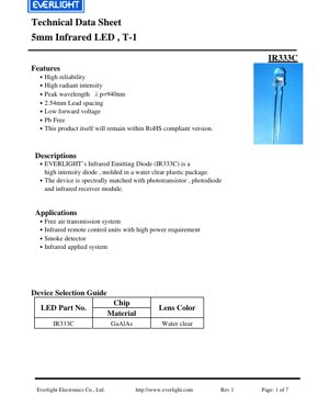
1. Product Overview
The IR333C is a high-intensity infrared emitting diode housed in a standard 5mm (T-1) water-clear plastic package. It is designed to emit light at a peak wavelength of 940nm, which is ideal for applications requiring non-visible light sources. The device is spectrally matched with common silicon phototransistors, photodiodes, and infrared receiver modules, ensuring optimal performance in signal transmission systems.
Key advantages of this component include its high reliability, high radiant intensity output, and low forward voltage requirement. The 2.54mm lead spacing makes it compatible with standard breadboards and PCBs. It is also manufactured as a Pb-Free and RoHS-compliant product, adhering to modern environmental standards.
1.1 Core Features and Target Market
The primary features that define the IR333C are its optical and electrical characteristics tailored for infrared applications. Its high radiant intensity, peaking at 940nm, makes it highly efficient for free-space optical communication. The low forward voltage reduces power consumption, which is critical for battery-operated devices.
The target applications are diverse and include:
- Free Air Transmission Systems: Used for short-range, wireless data links.
- Infrared Remote Control Units: Particularly those with high power requirements for longer range or through-obstacle operation.
- Smoke Detectors: Employed in optical chamber designs to detect smoke particles.
- General Infrared Applied Systems: This includes object sensing, proximity detection, and industrial automation.
2. In-Depth Technical Parameter Analysis
A thorough understanding of the device's specifications is crucial for reliable circuit design and system integration.
2.1 Absolute Maximum Ratings
These ratings define the limits beyond which permanent damage to the device may occur. They should never be exceeded, even momentarily.
- Continuous Forward Current (IF): 100 mA. This is the maximum DC current that can be passed through the LED indefinitely under specified conditions.
- Peak Forward Current (IFP): 1.0 A. This high current is permissible only under pulsed conditions (Pulse Width ≤ 100μs, Duty Cycle ≤ 1%). This is useful for achieving very high instantaneous radiant output.
- Reverse Voltage (VR): 5 V. The maximum voltage that can be applied in the reverse direction. Exceeding this can cause junction breakdown.
- Power Dissipation (Pd): 150 mW at or below 25°C. This rating considers both the forward voltage drop and the current. Operating above this limit will cause excessive heating and degrade performance or cause failure.
- Temperature Ranges: Operating and storage temperatures are specified from -40°C to +85°C, indicating suitability for industrial and automotive environments.
- Soldering Temperature (Tsol): 260°C for a maximum of 5 seconds. This is critical for wave or reflow soldering processes to prevent package damage.
2.2 Electro-Optical Characteristics
These parameters are measured under standard test conditions (Ta=25°C) and define the device's performance.
- Radiant Intensity (Ee): This is the optical power emitted per unit solid angle (mW/sr). The typical value is 15 mW/sr at IF=20mA. Under pulsed conditions of IF=100mA, it rises to 60 mW/sr, and at IF=1A, it reaches 450 mW/sr. This demonstrates the significant gain in output when using pulsed drive.
- Peak Wavelength (λp): 940 nm (typical). This is in the near-infrared spectrum, invisible to the human eye but efficiently detected by silicon-based sensors.
- Spectral Bandwidth (Δλ): 45 nm (typical). This defines the range of wavelengths emitted, centered around the peak. A narrower bandwidth can be beneficial for filtering out ambient light noise.
- Forward Voltage (VF): Typically 1.5V at IF=20mA, with a maximum of 1.85V at IF=100mA (pulsed). The low VF is a key advantage for low-voltage circuit design.
- Reverse Current (IR): Maximum 10 μA at VR=5V. This leakage current is very low.
- Viewing Angle (2θ1/2): 20 degrees (typical). This narrow beam angle concentrates the radiant intensity into a directed beam, increasing the effective range for applications like remote controls.
3. Binning System Explanation
The IR333C is sorted into different bins based on its radiant intensity at a standard test current of 20mA. This allows designers to select components with guaranteed minimum performance levels for their application.
The binning structure is as follows:
- Bin M: Radiant Intensity between 7.8 mW/sr (Min) and 12.5 mW/sr (Max).
- Bin N: Radiant Intensity between 11.0 mW/sr (Min) and 17.6 mW/sr (Max).
- Bin P: Radiant Intensity between 15.0 mW/sr (Min) and 24.0 mW/sr (Max).
- Bin Q: Radiant Intensity between 21.0 mW/sr (Min) and 34.0 mW/sr (Max).
For applications requiring consistent brightness or longer range, specifying a higher bin (e.g., P or Q) is recommended. The product label includes a \"CAT\" field to indicate the rank.
4. Performance Curve Analysis
The datasheet provides several characteristic curves that illustrate how parameters change with operating conditions.
4.1 Forward Current vs. Ambient Temperature (Fig. 1 & 8)
These curves show the relationship between the maximum allowable forward current and the ambient temperature. As temperature increases, the maximum permissible continuous current decreases linearly. This is due to the reduced power dissipation capability at higher temperatures. Designers must derate the operating current based on the expected maximum ambient temperature to ensure reliability.
4.2 Spectral Distribution (Fig. 2)
This graph plots relative intensity against wavelength. It confirms the peak emission at 940nm and shows the shape and width (approximately 45nm) of the emission spectrum. This is important for selecting appropriate optical filters in the receiver.
4.3 Peak Wavelength vs. Temperature (Fig. 3)
The peak emission wavelength has a slight temperature coefficient, typically shifting to longer wavelengths (red shift) as the junction temperature increases. This shift is usually small for infrared LEDs but should be considered in precision sensing applications.
4.4 Forward Current vs. Forward Voltage (Fig. 4)
This is the standard I-V curve for a diode. It shows the exponential relationship. The curve allows designers to determine the voltage drop for a given drive current, which is essential for calculating series resistor values or driver circuit requirements.
4.5 Relative Intensity vs. Forward Current (Fig. 5)
This curve demonstrates that the radiant output is approximately linear with forward current in the typical operating range. However, at very high currents, efficiency may drop due to heating and other effects.
4.6 Relative Radiant Intensity vs. Angular Displacement (Fig. 6)
This polar plot visually defines the viewing angle. The intensity is highest at 0 degrees (on-axis) and decreases as the angle increases, reaching half its maximum value at approximately ±10 degrees (hence the 20-degree full viewing angle).
5. Mechanical and Package Information
The device uses the industry-standard 5mm T-1 package. The lead spacing is 2.54mm (0.1 inches), which is the standard pitch for many prototyping boards and PCB layouts. The package is molded from water-clear plastic, which is transparent to the 940nm infrared light, minimizing optical losses. The cathode is typically identified by a flat spot on the plastic lens rim and/or a shorter lead. The detailed mechanical drawing in the datasheet provides all critical dimensions with tolerances, which are essential for PCB footprint design and ensuring proper fit in housings or lenses.
6. Soldering and Assembly Guidelines
To prevent damage during assembly, specific soldering conditions must be followed. The absolute maximum rating for soldering temperature is 260°C, and the soldering time must not exceed 5 seconds. This applies to both hand soldering and wave soldering processes. For reflow soldering, a profile that peaks at or below 260°C is required. Prolonged exposure to high temperature can crack the epoxy package or damage the internal wire bonds. It is also recommended to store the components in a dry environment to prevent moisture absorption, which can cause \"popcorning\" during reflow.
7. Packaging and Ordering Information
The standard packaging for the IR333C is as follows: 500 pieces are packed in one bag, 5 bags are placed in one box, and 10 boxes constitute one carton. This totals 25,000 pieces per carton. The product label contains several key fields for traceability and identification: CPN (Customer's Part Number), P/N (Manufacturer's Part Number), QTY (Quantity), CAT (Intensity Rank/Bin), HUE (Peak Wavelength), REF (Reference), and LOT No (Lot Number).
8. Application Design Suggestions
8.1 Typical Application Circuits
The most common drive circuit is a simple series resistor. The resistor value (Rs) is calculated using Ohm's Law: Rs = (Vsupply - VF) / IF. For example, to drive the LED at 20mA from a 5V supply with a typical VF of 1.5V: Rs = (5V - 1.5V) / 0.02A = 175Ω. A standard 180Ω resistor would be suitable. For pulsed operation at high currents (e.g., 1A), a transistor or MOSFET switch is necessary, often driven by a microcontroller.
8.2 Design Considerations
- Heat Management: While the package is small, at high continuous currents, power dissipation (Pd = VF * IF) can approach the 150mW limit. Ensure adequate ventilation or consider using a pulsed drive to reduce average power.
- Optical Design: The 20-degree viewing angle provides a focused beam. For wider coverage, a diffuser lens may be needed. Conversely, for very long-range applications, a secondary collimating lens can be used to narrow the beam further.
- Receiver Matching: Always pair the IR333C with a receiver (phototransistor, photodiode, or IC) that is sensitive in the 940nm region. Using an optical filter that blocks visible light can significantly improve signal-to-noise ratio in ambient light.
9. Technical Comparison and Differentiation
Compared to standard visible LEDs or other infrared LEDs, the IR333C's key differentiators are its combination of high pulsed output capability (450 mW/sr at 1A), low forward voltage, and narrow 20-degree beam angle. Some competing devices may offer wider viewing angles for broader coverage but at the expense of on-axis intensity. The 940nm wavelength is one of the most common and cost-effective, with good atmospheric transmission and abundant receiver options, compared to, for example, 850nm LEDs which have some visible red glow.
10. Frequently Asked Questions (FAQ)
Q: Can I drive this LED directly from a microcontroller pin?
A: For continuous operation at 20mA, check if your microcontroller's GPIO pin can source or sink that much current. Many can only handle 10-25mA. It is often safer to use a transistor as a switch.
Q: Why is the radiant intensity so much higher under pulsed conditions?
A> Pulsing the current allows you to drive the LED at currents far above its DC rating without overheating the junction. The light output is primarily a function of instantaneous current, so short, high-current pulses yield very bright flashes.
Q: How do I identify the cathode?
A: Look for the flat edge on the round plastic lens. The lead adjacent to this flat is the cathode. Also, the cathode lead is usually shorter than the anode lead.
Q: Is an infrared LED like this safe for eyes?
A> While invisible, infrared radiation can still be focused by the eye's lens onto the retina. For high-power applications, especially with lenses, it is prudent to avoid direct viewing. Most consumer remote controls use very low average power and are considered eye-safe.
11. Practical Use Case Example
Scenario: Long-Range Infrared Remote Control for a Gate Opener.
A designer needs a remote with a range of 50 meters in daylight. They select the IR333C in Bin Q for maximum intensity. The circuit uses a microcontroller to generate a 38kHz carrier signal, which is amplitude-modulated with the data code. An NPN transistor is used to pulse the LED at 1A with a very low duty cycle (e.g., 1%). A simple plastic lens is added in front of the LED to collimate the beam slightly. On the receiver side, a standard 38kHz IR receiver module with a 940nm filter is used. This design leverages the LED's high pulsed output and narrow beam to achieve the required range while maintaining low average power consumption for long battery life.
12. Operating Principle Introduction
An Infrared Light Emitting Diode (IR LED) is a semiconductor p-n junction diode. When a forward voltage is applied, electrons from the n-region and holes from the p-region are injected across the junction. When these charge carriers recombine, they release energy. In an IR LED, the semiconductor material (GaAlAs for the IR333C) is chosen so that this energy is released primarily as photons in the infrared portion of the electromagnetic spectrum (around 940nm). The water-clear epoxy package acts as a lens, shaping the emitted light into its characteristic beam pattern.
13. Technology Trends
The trend in infrared LEDs continues toward higher efficiency (more radiant output per electrical watt input) and higher power densities. This enables longer battery life and longer operational ranges in portable devices. There is also development in multi-wavelength and tunable IR sources for advanced sensing applications like gas analysis and spectroscopic measurement. Integration of the LED driver circuitry and even the sensor into compact modules is another common trend, simplifying design for end-users. The underlying drive for RoHS and green manufacturing standards remains strong across the industry.
LED Specification Terminology
Complete explanation of LED technical terms
Photoelectric Performance
| Term | Unit/Representation | Simple Explanation | Why Important |
|---|---|---|---|
| Luminous Efficacy | lm/W (lumens per watt) | Light output per watt of electricity, higher means more energy efficient. | Directly determines energy efficiency grade and electricity cost. |
| Luminous Flux | lm (lumens) | Total light emitted by source, commonly called "brightness". | Determines if the light is bright enough. |
| Viewing Angle | ° (degrees), e.g., 120° | Angle where light intensity drops to half, determines beam width. | Affects illumination range and uniformity. |
| CCT (Color Temperature) | K (Kelvin), e.g., 2700K/6500K | Warmth/coolness of light, lower values yellowish/warm, higher whitish/cool. | Determines lighting atmosphere and suitable scenarios. |
| CRI / Ra | Unitless, 0–100 | Ability to render object colors accurately, Ra≥80 is good. | Affects color authenticity, used in high-demand places like malls, museums. |
| SDCM | MacAdam ellipse steps, e.g., "5-step" | Color consistency metric, smaller steps mean more consistent color. | Ensures uniform color across same batch of LEDs. |
| Dominant Wavelength | nm (nanometers), e.g., 620nm (red) | Wavelength corresponding to color of colored LEDs. | Determines hue of red, yellow, green monochrome LEDs. |
| Spectral Distribution | Wavelength vs intensity curve | Shows intensity distribution across wavelengths. | Affects color rendering and quality. |
Electrical Parameters
| Term | Symbol | Simple Explanation | Design Considerations |
|---|---|---|---|
| Forward Voltage | Vf | Minimum voltage to turn on LED, like "starting threshold". | Driver voltage must be ≥Vf, voltages add up for series LEDs. |
| Forward Current | If | Current value for normal LED operation. | Usually constant current drive, current determines brightness & lifespan. |
| Max Pulse Current | Ifp | Peak current tolerable for short periods, used for dimming or flashing. | Pulse width & duty cycle must be strictly controlled to avoid damage. |
| Reverse Voltage | Vr | Max reverse voltage LED can withstand, beyond may cause breakdown. | Circuit must prevent reverse connection or voltage spikes. |
| Thermal Resistance | Rth (°C/W) | Resistance to heat transfer from chip to solder, lower is better. | High thermal resistance requires stronger heat dissipation. |
| ESD Immunity | V (HBM), e.g., 1000V | Ability to withstand electrostatic discharge, higher means less vulnerable. | Anti-static measures needed in production, especially for sensitive LEDs. |
Thermal Management & Reliability
| Term | Key Metric | Simple Explanation | Impact |
|---|---|---|---|
| Junction Temperature | Tj (°C) | Actual operating temperature inside LED chip. | Every 10°C reduction may double lifespan; too high causes light decay, color shift. |
| Lumen Depreciation | L70 / L80 (hours) | Time for brightness to drop to 70% or 80% of initial. | Directly defines LED "service life". |
| Lumen Maintenance | % (e.g., 70%) | Percentage of brightness retained after time. | Indicates brightness retention over long-term use. |
| Color Shift | Δu′v′ or MacAdam ellipse | Degree of color change during use. | Affects color consistency in lighting scenes. |
| Thermal Aging | Material degradation | Deterioration due to long-term high temperature. | May cause brightness drop, color change, or open-circuit failure. |
Packaging & Materials
| Term | Common Types | Simple Explanation | Features & Applications |
|---|---|---|---|
| Package Type | EMC, PPA, Ceramic | Housing material protecting chip, providing optical/thermal interface. | EMC: good heat resistance, low cost; Ceramic: better heat dissipation, longer life. |
| Chip Structure | Front, Flip Chip | Chip electrode arrangement. | Flip chip: better heat dissipation, higher efficacy, for high-power. |
| Phosphor Coating | YAG, Silicate, Nitride | Covers blue chip, converts some to yellow/red, mixes to white. | Different phosphors affect efficacy, CCT, and CRI. |
| Lens/Optics | Flat, Microlens, TIR | Optical structure on surface controlling light distribution. | Determines viewing angle and light distribution curve. |
Quality Control & Binning
| Term | Binning Content | Simple Explanation | Purpose |
|---|---|---|---|
| Luminous Flux Bin | Code e.g., 2G, 2H | Grouped by brightness, each group has min/max lumen values. | Ensures uniform brightness in same batch. |
| Voltage Bin | Code e.g., 6W, 6X | Grouped by forward voltage range. | Facilitates driver matching, improves system efficiency. |
| Color Bin | 5-step MacAdam ellipse | Grouped by color coordinates, ensuring tight range. | Guarantees color consistency, avoids uneven color within fixture. |
| CCT Bin | 2700K, 3000K etc. | Grouped by CCT, each has corresponding coordinate range. | Meets different scene CCT requirements. |
Testing & Certification
| Term | Standard/Test | Simple Explanation | Significance |
|---|---|---|---|
| LM-80 | Lumen maintenance test | Long-term lighting at constant temperature, recording brightness decay. | Used to estimate LED life (with TM-21). |
| TM-21 | Life estimation standard | Estimates life under actual conditions based on LM-80 data. | Provides scientific life prediction. |
| IESNA | Illuminating Engineering Society | Covers optical, electrical, thermal test methods. | Industry-recognized test basis. |
| RoHS / REACH | Environmental certification | Ensures no harmful substances (lead, mercury). | Market access requirement internationally. |
| ENERGY STAR / DLC | Energy efficiency certification | Energy efficiency and performance certification for lighting. | Used in government procurement, subsidy programs, enhances competitiveness. |