Table of Contents
- 1. Product Overview
- 1.1 Core Advantages and Target Market
- 2. In-Depth Technical Parameter Analysis
- 2.1 Absolute Maximum Ratings
- 2.2 Electro-Optical Characteristics
- 2.3 Transfer Characteristics
- 3. Performance Curve Analysis
- 4. Mechanical and Package Information
- 4.1 Package Dimensions and Variants
- 5. Soldering and Assembly Guidelines
- 6. Packaging and Ordering Information
- 7. Application Recommendations
- 7.1 Typical Application Circuits
- 7.2 Design Considerations and Best Practices
- 8. Technical Comparison and Selection Guide
- 9. Frequently Asked Questions (FAQ)
- 10. Practical Design Example
- 11. Operating Principle
- 12. Technology Trends
1. Product Overview
The 4N2X, 4N3X, and H11AX series are families of 6-pin Dual In-line Package (DIP) phototransistor photocouplers (also known as optocouplers or opto-isolators). Each device consists of a gallium arsenide infrared light-emitting diode (LED) optically coupled to a silicon phototransistor detector. This configuration provides complete electrical isolation between the input and output circuits, making them essential components for safety, noise immunity, and voltage level shifting in electronic systems.
The core function is signal transmission via light, eliminating a direct electrical connection. The input current energizes the infrared LED, which emits light proportional to the current. This light falls on the base region of the phototransistor, generating a base current and allowing collector-emitter current to flow, thereby replicating the input signal on the isolated output side.
1.1 Core Advantages and Target Market
These photocouplers are designed for applications requiring reliable signal isolation. Their key advantages include a high isolation voltage of 5000Vrms, which is critical for protecting low-voltage control circuits (like microprocessors) from high-voltage mains or motor drive sections. The extended creepage distance of >7.62mm further enhances safety and reliability in high-voltage environments. With an operating temperature range of -55°C to +110°C, they are suitable for industrial, automotive, and harsh environment applications.
The compact DIP package is available in standard, wide-lead spacing (0.4 inch), and surface-mount (SMD) variants, offering flexibility for through-hole and automated assembly processes. The devices carry approvals from major international safety agencies including UL, cUL, VDE, SEMKO, NEMKO, DEMKO, FIMKO, and CQC, facilitating their use in globally marketed equipment that must comply with stringent safety standards.
2. In-Depth Technical Parameter Analysis
The datasheet provides comprehensive electrical and optical specifications, which are crucial for proper circuit design and reliability assurance.
2.1 Absolute Maximum Ratings
These ratings define the stress limits beyond which permanent device damage may occur. They are not intended for normal operation.
- Input (LED) Side: Maximum continuous forward current (IF) is 60mA. A brief peak forward current (IFM) of 1A for 10µs is allowed, which is relevant for transient suppression. The maximum reverse voltage (VR) is a modest 6V, indicating the LED is not designed for high reverse bias and requires protection if used in AC circuits.
- Output (Phototransistor) Side: The collector-emitter and collector-base breakdown voltages (VCEO, VCBO) are both 80V, defining the maximum voltage that can be applied across the transistor in the off state. The emitter-base and emitter-collector voltages (VEBO, VECO) are limited to 7V.
- Power and Thermal: The total device power dissipation (PTOT) is 200mW at 25°C. Derating factors are provided: 3.8 mW/°C for the input side above 100°C and 9.0 mW/°C for the output side above 100°C. These are critical for calculating maximum allowable power at elevated ambient temperatures to prevent thermal runaway.
- Isolation: The isolation voltage (VISO) of 5000Vrms for 1 minute is a key safety parameter, tested with pins 1-2-3 shorted together and pins 4-5-6 shorted together.
2.2 Electro-Optical Characteristics
These parameters are measured under typical conditions (Ta=25°C) and define the device's performance.
- Input LED Characteristics: The forward voltage (VF) is typically 1.2V at IF=10mA, with a maximum of 1.5V. This is used to calculate the required current-limiting resistor. Reverse current (IR) is very low (<10µA at VR=6V). Input capacitance (Cin) is typically 30pF.
- Output Phototransistor Characteristics: Dark currents (ICBO, ICEO) are in the nanoampere range, indicating very low leakage when the LED is off. Breakdown voltages (BVCEO, BVCBO, etc.) confirm the 80V and 7V limits from the absolute ratings.
2.3 Transfer Characteristics
These parameters describe the coupling efficiency and switching performance between the input and output.
- Current Transfer Ratio (CTR): This is the most critical parameter, defined as (IC / IF) * 100%. It varies significantly by part number, creating a performance grading system:
- High CTR (>100%): 4N35, 4N36, 4N37.
- Medium-High CTR (50%): H11A1.
- Medium CTR (30%): H11A5.
- Standard CTR (20%): 4N25, 4N26, 4N38, H11A2, H11A3.
- Lower CTR (10%): 4N27, 4N28, H11A4.
- Saturation Voltage (VCE(sat)): This is the voltage drop across the phototransistor when it is fully turned on. Lower values (e.g., 0.3V max for 4N3X series at IF=10mA, IC=0.5mA) indicate better performance, minimizing power loss in the output stage.
- Switching Speed: Turn-on (ton) and turn-off (toff) times are specified for different series under specific test conditions (VCC=10V, RL=100Ω). The 4N2X/H11AX series are typically faster (3µs typ.) compared to the 4N3X series (10µs typ. for ton, 9µs typ. for toff). This is vital for digital signal transmission and PWM applications.
- Isolation Parameters: Isolation resistance (RIO) is extremely high (>1011 Ω), and input-output capacitance (CIO) is very low (0.2pF typ.), which minimizes capacitive coupling of high-frequency noise across the isolation barrier.
3. Performance Curve Analysis
While the PDF shows placeholder text for "Typical Electro-Optical Characteristics Curves," such curves are standard for photocouplers and typically include:
- Current Transfer Ratio (CTR) vs. Forward Current (IF): Shows how efficiency changes with LED drive current, often peaking at a specific current.
- CTR vs. Temperature: Illustrates the degradation of CTR at high temperatures, which is a critical derating factor for high-temperature operation.
- Collector Current (IC) vs. Collector-Emitter Voltage (VCE): Output characteristic curves showing the phototransistor's behavior in different regions (saturation, active).
- Switching Time vs. Load Resistance (RL): Demonstrates how the choice of pull-up resistor affects rise and fall times.
Designers should consult these curves from the full datasheet to optimize parameters like LED current, load resistor, and operating temperature for their specific speed and output requirements.
4. Mechanical and Package Information
The devices are offered in several 6-pin DIP package variants to suit different assembly needs.
4.1 Package Dimensions and Variants
The datasheet includes detailed mechanical drawings for each option. Key dimensions include overall length, width, pin spacing, and lead dimensions.
- Standard DIP Type: The classic through-hole package with 0.1-inch (2.54mm) row spacing.
- Option M Type: Features a "wide lead bend" providing 0.4-inch (10.16mm) lead spacing. This increases the creepage and clearance distance between input and output pins, enhancing isolation reliability for high-voltage applications.
- Option S & S1 Types: Surface-mount device (SMD) versions. Option S1 is a "low profile" variant, which has a reduced package height compared to the standard S option, beneficial for space-constrained applications.
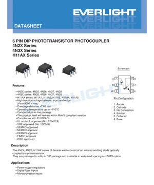
All packages feature a molded body that provides the necessary insulation. The pin configuration is standardized: Pin 1 (Anode), Pin 2 (Cathode), Pin 3 (NC), Pin 4 (Emitter), Pin 5 (Collector), Pin 6 (Base). The base pin (6) is often left unconnected but can be used for bandwidth improvement or bias control in some circuits.
5. Soldering and Assembly Guidelines
The absolute maximum ratings specify a soldering temperature (TSOL) of 260°C for 10 seconds. This is a typical value for wave or reflow soldering processes. For SMD options (S, S1), standard infrared or convection reflow profiles with a peak temperature around 260°C are applicable. It is crucial to avoid exceeding this time-temperature limit to prevent damage to the plastic package and internal wire bonds. Devices should be stored in conditions within the storage temperature range (-55°C to +125°C) and in moisture-sensitive packaging if specified for SMD parts to prevent "popcorning" during reflow.
6. Packaging and Ordering Information
The part numbering system is clearly defined: 4NXXY(Z)-V or H11AXY(Z)-V.
- XX / X: Specific part number (e.g., 25, 35, 1, 5).
- Y (Lead Form):
- None: Standard DIP (65 units/tube).
- M: Wide lead bend (65 units/tube).
- S: Surface mount lead form.
- S1: Low-profile surface mount lead form.
- Z (Tape & Reel): Applies only to SMD options.
- TA or TB: Different tape and reel specifications (1000 units/reel).
- V: Optional suffix indicating VDE safety approval.
This flexible system allows procurement of the exact mechanical variant required for production.
7. Application Recommendations
7.1 Typical Application Circuits
As listed in the datasheet, primary applications include:
- Power Supply Regulators: Providing feedback isolation in switch-mode power supplies (SMPS) between the secondary (output) side and the primary-side controller. This is essential for safety and noise rejection.
- Digital Logic Inputs / Microprocessor Inputs: Isolating noisy industrial sensor signals (e.g., from limit switches, encoders) or different ground domains before they enter sensitive digital logic or microcontroller pins.
- General Purpose Signal Isolation: Any circuit where two subsystems must communicate without sharing a common ground, to break ground loops, eliminate common-mode noise, or provide voltage level translation.
7.2 Design Considerations and Best Practices
- LED Current Limiting: Always use a series resistor to set the forward current (IF). Calculate Rlimit = (VCC_input - VF) / IF. Operate within the recommended IF range (often 5-20mA) for optimal CTR and longevity.
- Output Side Biasing: The phototransistor requires a pull-up resistor (RL) connected from the collector to VCC_output. Its value is a trade-off: a smaller RL provides faster switching but higher power consumption and lower output voltage swing; a larger RL gives better noise margin but slower speed.
- Speed Optimization: For faster switching, use a device from the faster series (4N2X/H11AX), minimize RL, and ensure adequate IF drive. Connecting a resistor (e.g., 100kΩ to 1MΩ) between the base (pin 6) and emitter can help bleed off stored charge and reduce turn-off time.
- Noise Immunity: The high isolation resistance and low capacitance inherently reject common-mode noise. For additional robustness in electrically noisy environments, bypass capacitors (e.g., 0.1µF) placed close to the device's supply pins on both input and output sides are recommended.
8. Technical Comparison and Selection Guide
The three series (4N2X, 4N3X, H11AX) offer a range of performance to meet different needs:
- 4N3X Series (4N35-38): Generally offer the highest CTR values (>100% for 4N35-37), making them suitable for applications requiring high output current or where minimal input drive current is desired. Their saturation voltage is also very low.
- 4N2X Series (4N25-28) & H11AX Series (H11A1-A5): Provide a graded range of CTR from 10% to 50%. The 4N2X series typically has faster switching times. These are versatile, general-purpose isolators. The H11A5 (30% CTR) and H11A1 (50% CTR) fill specific performance points.
- Selection Criteria: Choose based on required CTR (output current gain), switching speed, saturation voltage, and cost. For example, a microprocessor input reading a slow switch can use a lower-CTR, cost-effective part like the H11A4. A feedback loop in a power supply needing good linearity and gain might use a 4N35 or 4N36.
9. Frequently Asked Questions (FAQ)
Q: What is the purpose of the base pin (pin 6)?
A: The base pin provides access to the phototransistor's base region. Leaving it open (unconnected) is standard. Connecting a resistor from base to emitter can improve switching speed by providing a path to remove stored charge. In some designs, it can be used for pre-biasing or for connecting a speed-up network.
Q: How do I ensure long-term reliability?
A: Operate the LED within its absolute maximum ratings, preferably derated. Keep the junction temperature low by respecting the power derating curves. Use adequate creepage/clearance distances on your PCB, especially for the high-voltage isolation barrier, matching or exceeding the package's 7.62mm capability.
Q: Can I use this for AC signal isolation?
A: Yes, but the input LED has a low reverse voltage rating (6V). To isolate an AC signal, you must protect the LED from reverse bias, typically by placing a standard diode in inverse parallel across the LED input, or by using a bridge rectifier configuration before the LED.
Q: Why is CTR specified as a minimum value?
A> CTR has a wide variation due to manufacturing tolerances in LED efficiency and phototransistor gain. The datasheet guarantees a minimum CTR under specified conditions. Design must be based on this minimum value to ensure circuit functionality across all production units and over temperature.
10. Practical Design Example
Scenario: Isolating a 24V digital signal from a PLC output to a 3.3V microcontroller input.
- Device Selection: Choose a general-purpose part like the 4N25 (20% min CTR). Its speed is sufficient for digital I/O.
- Input Circuit: PLC output is 24V. Target IF = 10mA. VF ≈ 1.2V. Rlimit = (24V - 1.2V) / 0.01A = 2280Ω. Use a standard 2.2kΩ resistor. Add a reverse protection diode across the LED input.
- Output Circuit: Microcontroller VCC = 3.3V. Choose RL = 1kΩ. When the phototransistor is off, the output is pulled high to 3.3V (logic 1). When on, assuming IC = CTR * IF = 0.2 * 10mA = 2mA, the output voltage will be VCE(sat) (max 0.5V), a solid logic 0. The 1kΩ pull-up provides a good balance of speed and current consumption for this application.
11. Operating Principle
A photocoupler operates on the principle of electro-optical-electrical conversion. An electrical signal is applied to the input side, causing current to flow through an infrared LED. This current is directly proportional to the light intensity emitted. The light traverses a transparent insulating gap (typically a molded plastic) and strikes the semiconductor material of a photodetector—in this case, the base-collector junction of an NPN phototransistor. The photons generate electron-hole pairs, creating a base current. This photogenerated base current is then amplified by the transistor's current gain (hFE), resulting in a larger collector current that reproduces the original input signal on the electrically isolated output circuit. The complete absence of galvanic connection is what provides the high voltage isolation and noise immunity.
12. Technology Trends
Phototransistor-based photocouplers like the 4NXX series represent a mature and cost-effective isolation technology. Current trends in the optocoupler market include the development of devices with higher speed (for digital communication buses like SPI, I2C isolated with ICs specifically designed for this), higher integration (combining multiple channels or adding additional functions like gate drivers), and improved reliability metrics (higher temperature operation, longer lifetime). There is also growth in alternative isolation technologies such as capacitive isolators and giant magnetoresistance (GMR)-based isolators, which can offer advantages in size, speed, and power consumption for certain applications. However, phototransistor couplers remain dominant for general-purpose, cost-sensitive, and high-voltage isolation applications due to their simplicity, proven reliability, and excellent common-mode transient immunity (CMTI).
LED Specification Terminology
Complete explanation of LED technical terms
Photoelectric Performance
| Term | Unit/Representation | Simple Explanation | Why Important |
|---|---|---|---|
| Luminous Efficacy | lm/W (lumens per watt) | Light output per watt of electricity, higher means more energy efficient. | Directly determines energy efficiency grade and electricity cost. |
| Luminous Flux | lm (lumens) | Total light emitted by source, commonly called "brightness". | Determines if the light is bright enough. |
| Viewing Angle | ° (degrees), e.g., 120° | Angle where light intensity drops to half, determines beam width. | Affects illumination range and uniformity. |
| CCT (Color Temperature) | K (Kelvin), e.g., 2700K/6500K | Warmth/coolness of light, lower values yellowish/warm, higher whitish/cool. | Determines lighting atmosphere and suitable scenarios. |
| CRI / Ra | Unitless, 0–100 | Ability to render object colors accurately, Ra≥80 is good. | Affects color authenticity, used in high-demand places like malls, museums. |
| SDCM | MacAdam ellipse steps, e.g., "5-step" | Color consistency metric, smaller steps mean more consistent color. | Ensures uniform color across same batch of LEDs. |
| Dominant Wavelength | nm (nanometers), e.g., 620nm (red) | Wavelength corresponding to color of colored LEDs. | Determines hue of red, yellow, green monochrome LEDs. |
| Spectral Distribution | Wavelength vs intensity curve | Shows intensity distribution across wavelengths. | Affects color rendering and quality. |
Electrical Parameters
| Term | Symbol | Simple Explanation | Design Considerations |
|---|---|---|---|
| Forward Voltage | Vf | Minimum voltage to turn on LED, like "starting threshold". | Driver voltage must be ≥Vf, voltages add up for series LEDs. |
| Forward Current | If | Current value for normal LED operation. | Usually constant current drive, current determines brightness & lifespan. |
| Max Pulse Current | Ifp | Peak current tolerable for short periods, used for dimming or flashing. | Pulse width & duty cycle must be strictly controlled to avoid damage. |
| Reverse Voltage | Vr | Max reverse voltage LED can withstand, beyond may cause breakdown. | Circuit must prevent reverse connection or voltage spikes. |
| Thermal Resistance | Rth (°C/W) | Resistance to heat transfer from chip to solder, lower is better. | High thermal resistance requires stronger heat dissipation. |
| ESD Immunity | V (HBM), e.g., 1000V | Ability to withstand electrostatic discharge, higher means less vulnerable. | Anti-static measures needed in production, especially for sensitive LEDs. |
Thermal Management & Reliability
| Term | Key Metric | Simple Explanation | Impact |
|---|---|---|---|
| Junction Temperature | Tj (°C) | Actual operating temperature inside LED chip. | Every 10°C reduction may double lifespan; too high causes light decay, color shift. |
| Lumen Depreciation | L70 / L80 (hours) | Time for brightness to drop to 70% or 80% of initial. | Directly defines LED "service life". |
| Lumen Maintenance | % (e.g., 70%) | Percentage of brightness retained after time. | Indicates brightness retention over long-term use. |
| Color Shift | Δu′v′ or MacAdam ellipse | Degree of color change during use. | Affects color consistency in lighting scenes. |
| Thermal Aging | Material degradation | Deterioration due to long-term high temperature. | May cause brightness drop, color change, or open-circuit failure. |
Packaging & Materials
| Term | Common Types | Simple Explanation | Features & Applications |
|---|---|---|---|
| Package Type | EMC, PPA, Ceramic | Housing material protecting chip, providing optical/thermal interface. | EMC: good heat resistance, low cost; Ceramic: better heat dissipation, longer life. |
| Chip Structure | Front, Flip Chip | Chip electrode arrangement. | Flip chip: better heat dissipation, higher efficacy, for high-power. |
| Phosphor Coating | YAG, Silicate, Nitride | Covers blue chip, converts some to yellow/red, mixes to white. | Different phosphors affect efficacy, CCT, and CRI. |
| Lens/Optics | Flat, Microlens, TIR | Optical structure on surface controlling light distribution. | Determines viewing angle and light distribution curve. |
Quality Control & Binning
| Term | Binning Content | Simple Explanation | Purpose |
|---|---|---|---|
| Luminous Flux Bin | Code e.g., 2G, 2H | Grouped by brightness, each group has min/max lumen values. | Ensures uniform brightness in same batch. |
| Voltage Bin | Code e.g., 6W, 6X | Grouped by forward voltage range. | Facilitates driver matching, improves system efficiency. |
| Color Bin | 5-step MacAdam ellipse | Grouped by color coordinates, ensuring tight range. | Guarantees color consistency, avoids uneven color within fixture. |
| CCT Bin | 2700K, 3000K etc. | Grouped by CCT, each has corresponding coordinate range. | Meets different scene CCT requirements. |
Testing & Certification
| Term | Standard/Test | Simple Explanation | Significance |
|---|---|---|---|
| LM-80 | Lumen maintenance test | Long-term lighting at constant temperature, recording brightness decay. | Used to estimate LED life (with TM-21). |
| TM-21 | Life estimation standard | Estimates life under actual conditions based on LM-80 data. | Provides scientific life prediction. |
| IESNA | Illuminating Engineering Society | Covers optical, electrical, thermal test methods. | Industry-recognized test basis. |
| RoHS / REACH | Environmental certification | Ensures no harmful substances (lead, mercury). | Market access requirement internationally. |
| ENERGY STAR / DLC | Energy efficiency certification | Energy efficiency and performance certification for lighting. | Used in government procurement, subsidy programs, enhances competitiveness. |