Table of Contents
- 1. Product Overview
- 1.1 Core Advantages and Target Market
- 2. In-Depth Technical Parameter Analysis
- 2.1 Absolute Maximum Ratings
- 2.2 Electro-Optical Characteristics
- 2.2.1 Input Characteristics (Infrared LED)
- 2.2.2 Output Characteristics (Phototransistor)
- 2.3 Transfer Characteristics
- 2.4 Switching Characteristics
- 3. Grading System Explanation
- 4. Performance Curve Analysis
- 5. Mechanical and Package Information
- 5.1 Package Dimensions and Options
- 5.2 Pin Configuration and Polarity
- 6. Soldering and Assembly Guidelines
- 7. Packaging and Ordering Information
- 7.1 Model Numbering Rule
- 7.2 Packaging Specifications
- 8. Application Recommendations
- 8.1 Typical Application Circuits
- 8.2 Design Considerations
- 9. Technical Comparison
- 10. Frequently Asked Questions (Based on Technical Parameters)
- 11. Practical Design Example
- 12. Operating Principle
- 13. Technology Trends
- LED Specification Terminology
- Photoelectric Performance
- Electrical Parameters
- Thermal Management & Reliability
- Packaging & Materials
- Quality Control & Binning
- Testing & Certification
1. Product Overview
The CNY17-X and CNY17F-X series are families of 6-pin Dual In-line Package (DIP) photocouplers, also known as optocouplers or optoisolators. Each device consists of a gallium arsenide infrared light-emitting diode (LED) optically coupled to a silicon NPN phototransistor. The primary function is to provide electrical isolation between two circuits while allowing signal transmission via light. The key distinction between the two series is the availability of an external base connection (pin 6) in the CNY17-X, which is absent (No Connection) in the CNY17F-X series, the latter offering reduced noise susceptibility.
1.1 Core Advantages and Target Market
These devices are designed for applications requiring reliable signal isolation. Their core advantages include a high isolation voltage of 5000 Vrms, a compact DIP form factor suitable for through-hole mounting, and selected current transfer ratio (CTR) groupings for design consistency. They are approved by major international safety standards bodies (UL, cUL, VDE, SEMKO, etc.), making them suitable for a wide range of industrial, consumer, and power supply applications where safety and noise immunity are critical.
2. In-Depth Technical Parameter Analysis
2.1 Absolute Maximum Ratings
The Absolute Maximum Ratings define the stress limits beyond which permanent damage to the device may occur. These are not recommended operating conditions.
- Input (LED Side): The maximum continuous forward current (IF) is 60 mA. A short-duration (10 µs) peak forward current (IFM) of 1 A is permissible. The maximum reverse voltage (VR) across the LED is 6 V. The input power dissipation (PD) is 100 mW at 25°C, derating by 3.8 mW/°C above 100°C.
- Output (Phototransistor Side): The collector-emitter voltage (VCEO) and collector-base voltage (VCBO, for CNY17-X only) are rated at 80 V. The emitter-collector (VECO) and emitter-base (VEBO) voltages are 7 V. The output power dissipation (PC) is 150 mW at 25°C, derating by 9.0 mW/°C above 100°C.
- Device Total: The total device power dissipation (PTOT) must not exceed 200 mW.
- Isolation & Environment: The isolation voltage (VISO) is 5000 Vrms (AC for 1 minute). The operating temperature range (TOPR) is -55°C to +110°C. The maximum soldering temperature is 260°C for 10 seconds.
2.2 Electro-Optical Characteristics
These parameters define the device's performance under typical operating conditions (Ta = 25°C unless specified).
2.2.1 Input Characteristics (Infrared LED)
- Forward Voltage (VF): Maximum 1.65 V at IF = 60 mA. This is the voltage drop across the LED when conducting.
- Reverse Current (IR): Maximum 10 µA at VR = 6 V. This is the leakage current when the LED is reverse-biased.
- Input Capacitance (Cin): Typical 18 pF. This affects high-frequency switching performance on the input side.
2.2.2 Output Characteristics (Phototransistor)
- Dark Currents: With the LED off (IF=0), leakage currents exist. ICEO (collector-emitter) is typically 50 nA at VCE=10V. ICBO (collector-base, CNY17-X only) is max 20 nA at VCB=10V.
- Breakdown Voltages: BVCEO and BVCBO are min 80 V. BVECO is min 7 V.
- Output Capacitance (CCE): Typical 8 pF. This affects the output switching speed.
2.3 Transfer Characteristics
These are the most critical parameters for signal coupling applications.
- Current Transfer Ratio (CTR): This is the ratio of output collector current (IC) to input LED forward current (IF), expressed as a percentage. The devices are grouped into four distinct CTR ranges:
- CNY17-1 / CNY17F-1: CTR = 40% to 80% (at IF=10mA, VCE=5V)
- CNY17-2 / CNY17F-2: CTR = 63% to 125%
- CNY17-3 / CNY17F-3: CTR = 100% to 200%
- CNY17-4 / CNY17F-4: CTR = 160% to 320%
- CTR at Low Current: At IF = 1mA, the minimum CTR is specified (e.g., 13% for -1 grade, 56% for -4 grade), which is important for low-power or analog sensing applications.
- Saturation Voltage (VCE(sat)): Maximum 0.3 V at IF=10mA, IC=2.5mA. This is the voltage across the transistor when it is fully "on."
- Isolation Resistance (RIO): Minimum 1011 Ω. This indicates the extremely high DC resistance between the input and output sides.
- Input-Output Capacitance (CIO): Typical 0.5 pF. This small capacitance is key to achieving high common-mode transient immunity (CMTI).
2.4 Switching Characteristics
Dynamic performance is defined by turn-on/off and rise/fall times, which depend on test conditions.
- Condition 1 (VCC=10V, IC=2mA, RL=100Ω):
- Turn-on time (ton): Typical 10 µs, Max 12 µs.
- Turn-off time (toff): Typical 9 µs, Max 12 µs.
- Rise time (tr): Typical 6 µs, Max 10 µs.
- Fall time (tf): Typical 8 µs, Max 10 µs.
- Condition 2 (VCC=5V, IF=10mA, RL=75Ω):
- Rise time (tr): Typical 2 µs, Max 10 µs.
- Fall time (tf): Typical 3 µs, Max 10 µs.
3. Grading System Explanation
The primary grading for these photocouplers is based on the Current Transfer Ratio (CTR). The four grades (1, 2, 3, 4) offer progressively higher minimum and maximum CTR values. This allows designers to select a device that matches their required signal gain and provides consistency in production batches. For example, a digital input circuit requiring a strong, well-defined signal might use a -3 or -4 grade, while a circuit sensitive to variations might specify a tighter, lower-gain -1 grade.
4. Performance Curve Analysis
The datasheet references "Typical Electro-Optical Characteristics Curves." While the specific graphs are not detailed in the provided text, typical curves for such devices include:
- CTR vs. Forward Current (IF): Shows how the transfer ratio changes with LED drive current, usually peaking at a specific current.
- CTR vs. Temperature: Illustrates the decrease in CTR as ambient temperature increases, which is critical for high-temperature operation.
- Collector Current (IC) vs. Collector-Emitter Voltage (VCE): The output characteristics of the phototransistor, showing the saturation region and the active region.
- Forward Voltage (VF) vs. Forward Current (IF): The IV characteristic of the infrared LED.
These curves are essential for understanding device behavior under non-standard conditions and for optimizing circuit design.
5. Mechanical and Package Information
The devices are offered in a standard 6-pin DIP package with several lead form options.
5.1 Package Dimensions and Options
- Standard DIP: The default through-hole package.
- Option M: Features a "wide lead bend" providing 0.4 inch (approx. 10.16 mm) lead spacing for compatibility with wider PCB footprints.
- Option S: Surface mount lead form. Designed for reflow soldering processes.
- Option S1: Surface mount lead form with a "low profile" for applications with height restrictions.
Detailed dimensioned drawings (in mm) are provided for each option, specifying body size, pin length, pin spacing, and seating plane.
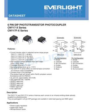
5.2 Pin Configuration and Polarity
Clear pin identification is crucial for correct installation.
- CNY17-X (with base pin):
- Anode (LED +)
- Cathode (LED -)
- No Connection
- Emitter (Phototransistor)
- Collector (Phototransistor)
- Base (Phototransistor, external connection)
- CNY17F-X (without base pin):
- Anode (LED +)
- Cathode (LED -)
- No Connection
- Emitter (Phototransistor)
- Collector (Phototransistor)
- No Connection
6. Soldering and Assembly Guidelines
The datasheet specifies a maximum soldering temperature of 260°C for 10 seconds. This is typically for wave or hand soldering of the through-hole leads. For surface mount options (S, S1), standard infrared or convection reflow profiles with a peak temperature not exceeding 260°C should be used. Precautions should be taken to avoid excessive mechanical stress on the package during handling. Storage should be in a dry, anti-static environment within the specified temperature range of -55°C to +125°C.
7. Packaging and Ordering Information
7.1 Model Numbering Rule
The part number follows the format: CNY17-XY(Z)-V or CNY17F-XY(Z)-V
- X: Part number / CTR grade (1, 2, 3, or 4).
- Y: Lead form option (S, S1, M, or none for Standard DIP).
- Z: Tape and reel option (TA, TB, or none). Applies only to S and S1 options.
- V: Optional VDE approval marking.
7.2 Packaging Specifications
- Tube Packaging: Standard DIP and Option M are supplied in tubes containing 65 units each.
- Tape and Reel: Options S and S1 are available on tape and reel. Both TA and TB options contain 1000 units per reel.
8. Application Recommendations
8.1 Typical Application Circuits
The datasheet lists common uses: Power supply regulators (for feedback isolation), digital logic inputs (for level shifting and noise isolation), and microprocessor inputs (for interfacing with noisy external signals). A specific test circuit for switching times is shown (Figure 11), which includes an input current-limiting resistor (RIN), an optional base-emitter resistor for the CNY17-X (RBE), and a collector load resistor (RL).
8.2 Design Considerations
- LED Current Limiting: Always use a series resistor to limit IF to the desired value, typically between 1 mA and 20 mA for a balance of speed, CTR, and power.
- Load Resistor (RL): The value of RL on the collector affects switching speed, output swing, and power consumption. A smaller RL gives faster fall times but reduces output voltage swing.
- Noise Immunity (CNY17F-X): The CNY17F-X series, with no external base connection, is less susceptible to noise injection into the phototransistor's base, making it preferable in electrically noisy environments.
- Speed vs. Current Trade-off: Higher IF generally improves switching speed but increases power dissipation. Refer to the switching time specifications under different test conditions.
- CTR Degradation: CTR can decrease over the lifetime of the device, especially at high operating temperatures and currents. Derate the design accordingly for long-term reliability.
9. Technical Comparison
The key differentiator within this family is the presence (CNY17-X) or absence (CNY17F-X) of the external base pin. The CNY17-X offers more design flexibility; the base pin can be left open, connected to the emitter via a resistor (to improve speed by sweeping out stored charge), or used in specific biasing configurations. The CNY17F-X offers superior noise immunity as the phototransistor base is completely internal and inaccessible, which is a significant advantage in high-noise industrial environments. Both series share identical isolation, voltage, and CTR specifications.
10. Frequently Asked Questions (Based on Technical Parameters)
Q: What is the main difference between grades -1, -2, -3, and -4?
A: The difference is the guaranteed range of the Current Transfer Ratio (CTR). Grade -4 has the highest gain (160-320%), while grade -1 has the lowest (40-80%). Choose based on the required signal amplification in your circuit.
Q: When should I use the CNY17F-X instead of the CNY17-X?
A: Use the CNY17F-X when operating in environments with significant electrical noise (e.g., motor drives, industrial controls). The lack of an external base connection makes it inherently less susceptible to electromagnetic interference (EMI) coupling into the sensitive base region.
Q: How do I calculate the input series resistor for the LED?
A: Use Ohm's Law: RIN = (VCC_IN - VF) / IF. Assume VF ≈ 1.2V typical (max 1.65V). For example, with a 5V supply and desired IF of 10mA: RIN = (5V - 1.2V) / 0.01A = 380Ω. Use a standard 390Ω resistor.
Q: Can I use this for AC signal isolation?
A: Yes, but with limitations. The phototransistor output is unidirectional (DC). To transmit AC signals, you typically need two photocouplers (one for each half-cycle) or additional circuitry to bias the output into its linear region for analog transmission, though linearity is not a specified parameter for this device.
11. Practical Design Example
Scenario: Isolating a 3.3V microcontroller GPIO pin from a 24V industrial sensor signal.
- Device Selection: Choose CNY17F-3 for good gain (100-200% CTR) and high noise immunity.
- Input Side (Microcontroller): GPIO pin drives the LED via a current-limiting resistor. With VGPIO_HIGH ≈ 3.3V and target IF = 5mA: RIN = (3.3V - 1.2V) / 0.005A = 420Ω. Use 430Ω.
- Output Side (Sensor Interface): Connect the phototransistor collector to the 24V supply via a pull-up resistor (RL). The emitter connects to ground. Choose RL to ensure the output saturates when on and provides a valid logic high when off. With IC ≈ CTR * IF = 150% * 5mA = 7.5mA (typical), and desired output logic high of ~20V when off: RL ≤ (24V - 20V) / (ICEO). With ICEO max ~50nA, almost any value works for leakage. For switching speed, a 10kΩ resistor is a common starting point. The output (collector node) now provides an isolated, inverted copy of the input signal.
12. Operating Principle
A photocoupler operates by converting an electrical signal into light, transmitting it across an electrically insulating barrier, and then converting the light back into an electrical signal. In the CNY17-X/F-X series, an electrical current (IF) flows through the infrared LED, causing it to emit photons. These photons pass through a transparent insulating mold compound and strike the base region of the silicon phototransistor. The photon energy generates electron-hole pairs in the base, creating a base current that turns on the transistor, allowing a collector current (IC) to flow. The ratio IC/IF is the CTR. No electrical connection exists between the input and output, providing galvanic isolation determined by the mold compound's dielectric strength and the internal pin spacing (creepage >7.6mm).
13. Technology Trends
Photocoupler technology continues to evolve. While traditional phototransistor-based couplers like the CNY17 series remain popular for cost-effective, general-purpose isolation, trends are moving towards:
Higher Speed: Development of faster couplers using photodiode and integrated amplifier (e.g., digital isolators) for multi-Mbps data transmission.
Higher Integration: Combining multiple isolation channels or integrating isolation with other functions like gate drivers or ADC interfaces in a single package.
Improved Reliability & Lifetime: Focus on materials and designs that minimize CTR degradation over time and temperature.
Miniaturization: Migration to smaller surface-mount packages (SOIC, SSOP) with the same or better isolation ratings. The CNY17 series' S and S1 options reflect this trend towards surface-mount assembly.
LED Specification Terminology
Complete explanation of LED technical terms
Photoelectric Performance
| Term | Unit/Representation | Simple Explanation | Why Important |
|---|---|---|---|
| Luminous Efficacy | lm/W (lumens per watt) | Light output per watt of electricity, higher means more energy efficient. | Directly determines energy efficiency grade and electricity cost. |
| Luminous Flux | lm (lumens) | Total light emitted by source, commonly called "brightness". | Determines if the light is bright enough. |
| Viewing Angle | ° (degrees), e.g., 120° | Angle where light intensity drops to half, determines beam width. | Affects illumination range and uniformity. |
| CCT (Color Temperature) | K (Kelvin), e.g., 2700K/6500K | Warmth/coolness of light, lower values yellowish/warm, higher whitish/cool. | Determines lighting atmosphere and suitable scenarios. |
| CRI / Ra | Unitless, 0–100 | Ability to render object colors accurately, Ra≥80 is good. | Affects color authenticity, used in high-demand places like malls, museums. |
| SDCM | MacAdam ellipse steps, e.g., "5-step" | Color consistency metric, smaller steps mean more consistent color. | Ensures uniform color across same batch of LEDs. |
| Dominant Wavelength | nm (nanometers), e.g., 620nm (red) | Wavelength corresponding to color of colored LEDs. | Determines hue of red, yellow, green monochrome LEDs. |
| Spectral Distribution | Wavelength vs intensity curve | Shows intensity distribution across wavelengths. | Affects color rendering and quality. |
Electrical Parameters
| Term | Symbol | Simple Explanation | Design Considerations |
|---|---|---|---|
| Forward Voltage | Vf | Minimum voltage to turn on LED, like "starting threshold". | Driver voltage must be ≥Vf, voltages add up for series LEDs. |
| Forward Current | If | Current value for normal LED operation. | Usually constant current drive, current determines brightness & lifespan. |
| Max Pulse Current | Ifp | Peak current tolerable for short periods, used for dimming or flashing. | Pulse width & duty cycle must be strictly controlled to avoid damage. |
| Reverse Voltage | Vr | Max reverse voltage LED can withstand, beyond may cause breakdown. | Circuit must prevent reverse connection or voltage spikes. |
| Thermal Resistance | Rth (°C/W) | Resistance to heat transfer from chip to solder, lower is better. | High thermal resistance requires stronger heat dissipation. |
| ESD Immunity | V (HBM), e.g., 1000V | Ability to withstand electrostatic discharge, higher means less vulnerable. | Anti-static measures needed in production, especially for sensitive LEDs. |
Thermal Management & Reliability
| Term | Key Metric | Simple Explanation | Impact |
|---|---|---|---|
| Junction Temperature | Tj (°C) | Actual operating temperature inside LED chip. | Every 10°C reduction may double lifespan; too high causes light decay, color shift. |
| Lumen Depreciation | L70 / L80 (hours) | Time for brightness to drop to 70% or 80% of initial. | Directly defines LED "service life". |
| Lumen Maintenance | % (e.g., 70%) | Percentage of brightness retained after time. | Indicates brightness retention over long-term use. |
| Color Shift | Δu′v′ or MacAdam ellipse | Degree of color change during use. | Affects color consistency in lighting scenes. |
| Thermal Aging | Material degradation | Deterioration due to long-term high temperature. | May cause brightness drop, color change, or open-circuit failure. |
Packaging & Materials
| Term | Common Types | Simple Explanation | Features & Applications |
|---|---|---|---|
| Package Type | EMC, PPA, Ceramic | Housing material protecting chip, providing optical/thermal interface. | EMC: good heat resistance, low cost; Ceramic: better heat dissipation, longer life. |
| Chip Structure | Front, Flip Chip | Chip electrode arrangement. | Flip chip: better heat dissipation, higher efficacy, for high-power. |
| Phosphor Coating | YAG, Silicate, Nitride | Covers blue chip, converts some to yellow/red, mixes to white. | Different phosphors affect efficacy, CCT, and CRI. |
| Lens/Optics | Flat, Microlens, TIR | Optical structure on surface controlling light distribution. | Determines viewing angle and light distribution curve. |
Quality Control & Binning
| Term | Binning Content | Simple Explanation | Purpose |
|---|---|---|---|
| Luminous Flux Bin | Code e.g., 2G, 2H | Grouped by brightness, each group has min/max lumen values. | Ensures uniform brightness in same batch. |
| Voltage Bin | Code e.g., 6W, 6X | Grouped by forward voltage range. | Facilitates driver matching, improves system efficiency. |
| Color Bin | 5-step MacAdam ellipse | Grouped by color coordinates, ensuring tight range. | Guarantees color consistency, avoids uneven color within fixture. |
| CCT Bin | 2700K, 3000K etc. | Grouped by CCT, each has corresponding coordinate range. | Meets different scene CCT requirements. |
Testing & Certification
| Term | Standard/Test | Simple Explanation | Significance |
|---|---|---|---|
| LM-80 | Lumen maintenance test | Long-term lighting at constant temperature, recording brightness decay. | Used to estimate LED life (with TM-21). |
| TM-21 | Life estimation standard | Estimates life under actual conditions based on LM-80 data. | Provides scientific life prediction. |
| IESNA | Illuminating Engineering Society | Covers optical, electrical, thermal test methods. | Industry-recognized test basis. |
| RoHS / REACH | Environmental certification | Ensures no harmful substances (lead, mercury). | Market access requirement internationally. |
| ENERGY STAR / DLC | Energy efficiency certification | Energy efficiency and performance certification for lighting. | Used in government procurement, subsidy programs, enhances competitiveness. |