1. Product Overview
This document details the specifications for a high-performance Silicon Carbide (SiC) Schottky Barrier Diode (SBD) housed in a TO-220-2L package. The device is engineered for high-voltage, high-frequency power conversion applications where efficiency, thermal management, and switching speed are critical. SiC technology offers significant advantages over traditional silicon diodes, primarily due to its superior material properties.
The core function of this diode is to allow current to flow in one direction (from anode to cathode) with minimal forward voltage drop and to block high reverse voltages with very low leakage current. Its key differentiator is the near-zero reverse recovery charge, which is a fundamental limitation of silicon PN junction diodes. This characteristic makes it ideal for circuits operating at elevated switching frequencies.
1.1 Core Advantages and Target Market
The primary benefits of this SiC Schottky diode stem from its material and structural properties. The low forward voltage (VF) reduces conduction losses, directly improving system efficiency. The absence of significant minority carrier storage eliminates reverse recovery losses, enabling high-speed switching without the associated switching losses and electromagnetic interference (EMI) typical of silicon fast recovery diodes. This allows for the design of smaller, lighter, and more efficient power systems by enabling higher operating frequencies, which in turn reduces the size of passive components like inductors and transformers.
The high surge current capability and maximum junction temperature of 175°C enhance system robustness and reliability. The device is also compliant with environmental standards (Pb-Free, Halogen Free, RoHS). These features make it particularly suitable for demanding applications in modern power electronics. The target markets include industrial power supplies, renewable energy systems, and critical infrastructure power management.
2. In-Depth Technical Parameter Analysis
A thorough understanding of the electrical and thermal parameters is essential for reliable circuit design and ensuring the device operates within its safe operating area (SOA).
2.1 Absolute Maximum Ratings
These ratings define the stress limits that, if exceeded, may cause permanent damage to the device. They are not intended for normal operating conditions.
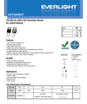
- Repetitive Peak Reverse Voltage (VRRM): 650V. This is the maximum reverse voltage that can be applied repetitively.
- Continuous Forward Current (IF): 10A. This is the maximum DC current the device can handle continuously, limited by the thermal resistance and maximum junction temperature.
- Surge Non-Repetitive Forward Current (IFSM): 30A (TC=25°C, tp=10ms, sine half-wave). This rating indicates the diode's ability to withstand short-duration overload currents, such as those encountered during startup or fault conditions.
- Junction Temperature (TJ): 175°C maximum. Operating the device at or near this limit will reduce its long-term reliability.
- Total Power Dissipation (PD): 88W (TC=25°C). This value is derived from the thermal resistance and the maximum allowable temperature rise.
2.2 Electrical Characteristics
These are the typical and maximum/minimum performance parameters under specified test conditions.
- Forward Voltage (VF): 1.48V typical, 1.85V maximum at IF=10A, TJ=25°C. This parameter increases with temperature, reaching approximately 1.9V at TJ=175°C. The low VF is a key advantage for reducing conduction losses.
- Reverse Current (IR): 2µA typical, 60µA maximum at VR=520V, TJ=25°C. Leakage current increases significantly with temperature (20µA typical at 175°C), which must be considered in thermal design.
- Total Capacitive Charge (QC): 15nC typical at VR=400V, TJ=25°C. This is a critical parameter for switching loss calculation in high-frequency applications. The low QC value confirms the minimal switching losses associated with this Schottky device.
- Total Capacitance (Ct): This is voltage-dependent. Typical values are 256pF at VR=1V, 29pF at VR=200V, and 23pF at VR=400V (f=1MHz). The decreasing capacitance with increasing reverse voltage is characteristic of junction capacitance.
2.3 Thermal Characteristics
Effective heat dissipation is crucial for maintaining performance and reliability.
- Thermal Resistance, Junction-to-Case (RθJC): 1.7°C/W typical. This low value indicates efficient heat transfer from the semiconductor junction to the metal tab (case) of the TO-220 package. The case must be properly attached to a heatsink to utilize this characteristic fully. The maximum value is not specified, so designers should use the typical value with appropriate derating factors.
3. Performance Curve Analysis
The datasheet provides several graphical representations of device behavior, which are essential for detailed design analysis beyond the tabulated data points.
3.1 VF-IF Characteristics
This curve shows the relationship between forward voltage and forward current at different junction temperatures. It visually demonstrates the positive temperature coefficient of VF. This characteristic is beneficial for current sharing when multiple diodes are connected in parallel, as it provides a degree of self-balancing and helps prevent thermal runaway.
3.2 VR-IR Characteristics
This graph plots reverse leakage current against reverse voltage, typically at multiple temperatures. It highlights the exponential increase in leakage current with both voltage and temperature, informing designers about off-state losses and thermal stability under high blocking voltage.
3.3 Maximum Ip – TC Characteristics
This derating curve shows how the maximum allowable continuous forward current (Ip) decreases as the case temperature (TC) increases. It is a direct application of the power dissipation and thermal resistance limits. Designers must use this graph to select an appropriate heatsink based on their operating ambient temperature and required current.
3.4 Transient Thermal Resistance
The curve of transient thermal resistance versus pulse width (ZθJC) is critical for evaluating temperature rise during short current pulses, such as those in switching applications. It shows that for very short pulses, the effective thermal resistance is lower than the steady-state value, allowing the device to handle higher peak power for brief durations.
4. Mechanical and Package Information
The device uses the industry-standard TO-220-2L package, which is designed for through-hole mounting with screw attachment to a heatsink.
4.1 Package Dimensions and Outline
The detailed mechanical drawing provides all critical dimensions in millimeters. Key package body dimensions are approximately 15.6mm (D) x 9.99mm (E) x 4.5mm (A). The lead pitch (distance between pin centers) is 5.08mm (e1). The mounting hole dimensions and tab size are also specified to ensure proper mechanical and thermal interface with the heatsink.
4.2 Pin Configuration and Polarity Identification
The device has two leads (2L). Pin 1 is the Cathode (K), and Pin 2 is the Anode (A). Importantly, the metal tab or case of the TO-220 package is electrically connected to the Cathode. This must be considered during assembly to prevent short circuits, as the heatsink is typically at ground potential. Proper insulation (e.g., a mica or silicone insulator with a thermal pad) is required if the heatsink is not at cathode potential.
4.3 Recommended PCB Land Pattern
A suggested pad layout for surface-mounting the leads (after forming) is provided. This aids in PCB design for wave or reflow soldering processes, ensuring reliable solder joints and proper mechanical support.
5. Application Guidelines and Design Considerations
5.1 Typical Application Circuits
This diode is specifically advantageous in several key power conversion topologies:
- Power Factor Correction (PFC): In boost PFC stages, the diode's fast switching and low recovery losses are crucial for high efficiency at high line frequencies, helping to meet stringent efficiency standards like 80 PLUS.
- Solar Inverters: Used in the boost stage or as freewheeling diodes, they minimize losses, increasing the overall energy harvest from photovoltaic panels.
- Uninterruptible Power Supplies (UPS) & Motor Drives: In the output inverter stages or as clamp/freewheeling diodes, they reduce switching losses, allowing for higher switching frequencies which can lead to smaller magnetic components and improved output waveform quality.
- Data Center Power Supplies: High efficiency is paramount for reducing operational costs (electricity) and cooling requirements. This diode contributes directly to achieving high power density and efficiency in server power supplies.
5.2 Critical Design Considerations
- Heatsinking: The low RθJC is only effective with an adequate heatsink. The mounting torque for the screw (M3 or 6-32) is specified as 8.8 N·m (approximately 78 lbf-in) to ensure optimal thermal contact without damaging the package.
- Parallel Operation: The positive temperature coefficient of VF facilitates parallel connection for higher current capability. However, careful attention to layout symmetry (equal length traces) and shared heatsinking is still recommended to ensure balanced current sharing.
- Voltage Stresses: In circuits with inductive loads or parasitic inductance, voltage spikes exceeding VRRM can occur during turn-off. Snubber circuits or RC dampers may be necessary to clamp these spikes and protect the diode.
- ESD and Handling: While more robust than some semiconductors, Schottky diodes can be sensitive to electrostatic discharge. Standard ESD precautions should be observed during handling and assembly.
6. Technical Comparison and Trends
6.1 Comparison with Silicon Diodes
Compared to a silicon fast recovery diode (FRD) of similar voltage and current rating, this SiC Schottky diode offers: 1) Dramatically lower reverse recovery charge (Qrr) and time (trr), essentially eliminating reverse recovery losses and associated noise. 2) A higher maximum operating junction temperature (175°C vs. typically 150°C for silicon). 3) A slightly higher forward voltage drop, but this is often outweighed by the switching loss savings at frequencies above ~30kHz. The system-level benefits include smaller heatsinks, smaller magnetics, and higher overall efficiency.
6.2 Principle of Operation and Trends
A Schottky diode is formed by a metal-semiconductor junction, as opposed to a PN junction. This majority-carrier device has no minority carrier storage, which is the root cause of its fast switching speed. Silicon Carbide (SiC) as the semiconductor material provides a wider bandgap than silicon, resulting in higher breakdown field strength, higher thermal conductivity, and higher maximum operating temperature. The trend in power electronics is strongly towards wide-bandgap semiconductors like SiC and Gallium Nitride (GaN) to push the boundaries of efficiency, frequency, and power density. This diode represents a mature and widely adopted component within that trend, particularly for high-voltage applications where SiC's advantages are most pronounced.
7. Frequently Asked Questions (FAQ)
Q: Can this diode be used directly as a replacement for a silicon fast recovery diode in an existing design?
A: Not directly without evaluation. While the pinout may be compatible, the differences in forward voltage, switching behavior, and the need for a cathode-isolated heatsink (if the original design had the tab connected to a non-cathode potential) must be carefully reviewed. Circuit simulation and testing are strongly recommended.
Q: What is the significance of the QC (Total Capacitive Charge) parameter?
A> QC represents the charge associated with the junction capacitance. During high-frequency switching, this capacitance must be charged and discharged each cycle, resulting in a capacitive switching loss proportional to QC * V * f. The low QC value of this SiC diode minimizes these losses, which become significant at very high frequencies.
Q: How does the positive temperature coefficient of VF prevent thermal runaway in parallel configurations?
A: If one diode in a parallel pair starts to draw more current, it heats up. Its VF increases due to the positive temperature coefficient, which in turn reduces the voltage difference driving current through it relative to the cooler diode. This natural feedback mechanism encourages current to shift back to the cooler diode, promoting balance.
Q: What are the storage and handling requirements?
A: The device should be stored in an anti-static bag in an environment with a temperature range of -55°C to +175°C and low humidity. Standard IPC/JEDEC guidelines for handling moisture-sensitive components (if applicable) and ESD-sensitive devices should be followed.
LED Specification Terminology
Complete explanation of LED technical terms
Photoelectric Performance
| Term | Unit/Representation | Simple Explanation | Why Important |
|---|---|---|---|
| Luminous Efficacy | lm/W (lumens per watt) | Light output per watt of electricity, higher means more energy efficient. | Directly determines energy efficiency grade and electricity cost. |
| Luminous Flux | lm (lumens) | Total light emitted by source, commonly called "brightness". | Determines if the light is bright enough. |
| Viewing Angle | ° (degrees), e.g., 120° | Angle where light intensity drops to half, determines beam width. | Affects illumination range and uniformity. |
| CCT (Color Temperature) | K (Kelvin), e.g., 2700K/6500K | Warmth/coolness of light, lower values yellowish/warm, higher whitish/cool. | Determines lighting atmosphere and suitable scenarios. |
| CRI / Ra | Unitless, 0–100 | Ability to render object colors accurately, Ra≥80 is good. | Affects color authenticity, used in high-demand places like malls, museums. |
| SDCM | MacAdam ellipse steps, e.g., "5-step" | Color consistency metric, smaller steps mean more consistent color. | Ensures uniform color across same batch of LEDs. |
| Dominant Wavelength | nm (nanometers), e.g., 620nm (red) | Wavelength corresponding to color of colored LEDs. | Determines hue of red, yellow, green monochrome LEDs. |
| Spectral Distribution | Wavelength vs intensity curve | Shows intensity distribution across wavelengths. | Affects color rendering and quality. |
Electrical Parameters
| Term | Symbol | Simple Explanation | Design Considerations |
|---|---|---|---|
| Forward Voltage | Vf | Minimum voltage to turn on LED, like "starting threshold". | Driver voltage must be ≥Vf, voltages add up for series LEDs. |
| Forward Current | If | Current value for normal LED operation. | Usually constant current drive, current determines brightness & lifespan. |
| Max Pulse Current | Ifp | Peak current tolerable for short periods, used for dimming or flashing. | Pulse width & duty cycle must be strictly controlled to avoid damage. |
| Reverse Voltage | Vr | Max reverse voltage LED can withstand, beyond may cause breakdown. | Circuit must prevent reverse connection or voltage spikes. |
| Thermal Resistance | Rth (°C/W) | Resistance to heat transfer from chip to solder, lower is better. | High thermal resistance requires stronger heat dissipation. |
| ESD Immunity | V (HBM), e.g., 1000V | Ability to withstand electrostatic discharge, higher means less vulnerable. | Anti-static measures needed in production, especially for sensitive LEDs. |
Thermal Management & Reliability
| Term | Key Metric | Simple Explanation | Impact |
|---|---|---|---|
| Junction Temperature | Tj (°C) | Actual operating temperature inside LED chip. | Every 10°C reduction may double lifespan; too high causes light decay, color shift. |
| Lumen Depreciation | L70 / L80 (hours) | Time for brightness to drop to 70% or 80% of initial. | Directly defines LED "service life". |
| Lumen Maintenance | % (e.g., 70%) | Percentage of brightness retained after time. | Indicates brightness retention over long-term use. |
| Color Shift | Δu′v′ or MacAdam ellipse | Degree of color change during use. | Affects color consistency in lighting scenes. |
| Thermal Aging | Material degradation | Deterioration due to long-term high temperature. | May cause brightness drop, color change, or open-circuit failure. |
Packaging & Materials
| Term | Common Types | Simple Explanation | Features & Applications |
|---|---|---|---|
| Package Type | EMC, PPA, Ceramic | Housing material protecting chip, providing optical/thermal interface. | EMC: good heat resistance, low cost; Ceramic: better heat dissipation, longer life. |
| Chip Structure | Front, Flip Chip | Chip electrode arrangement. | Flip chip: better heat dissipation, higher efficacy, for high-power. |
| Phosphor Coating | YAG, Silicate, Nitride | Covers blue chip, converts some to yellow/red, mixes to white. | Different phosphors affect efficacy, CCT, and CRI. |
| Lens/Optics | Flat, Microlens, TIR | Optical structure on surface controlling light distribution. | Determines viewing angle and light distribution curve. |
Quality Control & Binning
| Term | Binning Content | Simple Explanation | Purpose |
|---|---|---|---|
| Luminous Flux Bin | Code e.g., 2G, 2H | Grouped by brightness, each group has min/max lumen values. | Ensures uniform brightness in same batch. |
| Voltage Bin | Code e.g., 6W, 6X | Grouped by forward voltage range. | Facilitates driver matching, improves system efficiency. |
| Color Bin | 5-step MacAdam ellipse | Grouped by color coordinates, ensuring tight range. | Guarantees color consistency, avoids uneven color within fixture. |
| CCT Bin | 2700K, 3000K etc. | Grouped by CCT, each has corresponding coordinate range. | Meets different scene CCT requirements. |
Testing & Certification
| Term | Standard/Test | Simple Explanation | Significance |
|---|---|---|---|
| LM-80 | Lumen maintenance test | Long-term lighting at constant temperature, recording brightness decay. | Used to estimate LED life (with TM-21). |
| TM-21 | Life estimation standard | Estimates life under actual conditions based on LM-80 data. | Provides scientific life prediction. |
| IESNA | Illuminating Engineering Society | Covers optical, electrical, thermal test methods. | Industry-recognized test basis. |
| RoHS / REACH | Environmental certification | Ensures no harmful substances (lead, mercury). | Market access requirement internationally. |
| ENERGY STAR / DLC | Energy efficiency certification | Energy efficiency and performance certification for lighting. | Used in government procurement, subsidy programs, enhances competitiveness. |