Table of Contents
- 1. Product Overview
- 1.1 Key Features and Benefits
- 2. In-Depth Technical Parameter Analysis
- 2.1 Absolute Maximum Ratings
- 2.2 Electrical Characteristics
- 2.3 Thermal Characteristics
- 3. Performance Curve Analysis
- 3.1 VF-IF Characteristics
- 3.2 VR-IR Characteristics
- 3.3 Maximum Forward Current vs. Case Temperature
- 3.4 Transient Thermal Impedance
- 4. Mechanical and Package Information
- 4.1 Package Outline and Dimensions
- 4.2 Pin Configuration and Polarity
- 4.3 Recommended PCB Land Pattern
- 5. Application Guidelines and Design Considerations
- 5.1 Typical Application Circuits
- 5.2 Heatsinking and Thermal Design
- 5.3 Layout Considerations
- 6. Technology Comparison and Differentiation
- 6.1 vs. Silicon PN Junction Diodes
- 6.2 vs. Silicon Carbide MOSFET Body Diode
- 7. Frequently Asked Questions (FAQs)
- 8. Technical Principles and Trends
- 8.1 Operating Principle of a SiC Schottky Diode
- 8.2 Industry Trends
- LED Specification Terminology
- Photoelectric Performance
- Electrical Parameters
- Thermal Management & Reliability
- Packaging & Materials
- Quality Control & Binning
- Testing & Certification
1. Product Overview
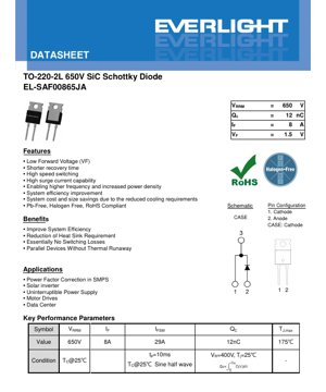
The EL-SAF008 65JA is a Silicon Carbide (SiC) Schottky Barrier Diode (SBD) designed for high-efficiency, high-frequency power conversion applications. Encapsulated in a standard TO-220-2L package, this device leverages the superior material properties of Silicon Carbide to offer significant performance advantages over conventional silicon-based diodes, particularly in systems requiring high voltage, fast switching, and improved thermal management.
The core advantage of SiC technology lies in its wide bandgap, which enables the diode to operate at much higher temperatures, voltages, and switching frequencies. This device is engineered to minimize switching losses and conduction losses, contributing directly to increased power density and overall system efficiency. Its primary target markets include advanced switch-mode power supplies (SMPS), renewable energy inverters, motor drives, and critical infrastructure power systems like data centers and uninterruptible power supplies (UPS).
1.1 Key Features and Benefits
The device incorporates several design features that translate into tangible system-level benefits:
- Low Forward Voltage (VF): Typically 1.5V at 8A and 25°C. This reduces conduction losses, leading to cooler operation and higher efficiency.
- Essentially No Reverse Recovery Charge (Qc): A defining characteristic of Schottky diodes, with a specified Qc of only 12nC. This eliminates reverse recovery losses, a major source of switching loss in silicon PN junction diodes, enabling high-speed switching.
- High Surge Current Capability (IFSM): Rated for 29A non-repetitive surge current (10ms half-sine wave). This provides robustness against inrush currents and short-term overloads.
- High Junction Temperature (TJ,max): Rated for operation up to 175°C. This allows for operation in high ambient temperatures or enables the use of smaller heatsinks.
- Parallel Operation: The positive temperature coefficient of the forward voltage drop helps prevent thermal runaway, making the device suitable for parallel connection to handle higher currents.
- Environmental Compliance: The device is Pb-Free, Halogen Free, and RoHS Compliant, meeting modern environmental standards.
The combined benefits are substantial: improved system efficiency, reduced cooling requirements (leading to smaller system size and cost), and the ability to operate at higher frequencies for magnetics miniaturization.
2. In-Depth Technical Parameter Analysis
This section provides a detailed, objective interpretation of the key electrical and thermal parameters specified in the datasheet.
2.1 Absolute Maximum Ratings
These ratings define the stress limits beyond which permanent damage to the device may occur. Operation at or beyond these limits is not guaranteed.
- Repetitive Peak Reverse Voltage (VRRM): 650V. This is the maximum instantaneous reverse voltage that can be applied repetitively.
- DC Blocking Voltage (VR): 650V. The maximum continuous reverse DC voltage.
- Continuous Forward Current (IF): 8A. This is the maximum continuous forward current, limited by the maximum junction temperature and the thermal resistance from junction to case (Rth(JC)).
- Surge Non-Repetitive Forward Current (IFSM): 29A (TC=25°C, tp=10ms, half-sine wave). This rating is crucial for assessing the diode's ability to withstand short-circuit or startup surge conditions.
- Junction Temperature (TJ): -55°C to +175°C. The operating and storage temperature range for the semiconductor die itself.
2.2 Electrical Characteristics
These are the guaranteed performance parameters under specified test conditions.
- Forward Voltage (VF): Max 1.85V at IF=8A across the full temperature range (25°C to 175°C). The typical value is 1.5V at 25°C. It is important to note that VF has a positive temperature coefficient.
- Reverse Leakage Current (IR): Max 40µA at VR=520V, TJ=25°C. This increases with temperature, with a max of 20µA at 175°C under the same VR. Low leakage is critical for efficiency in blocking states.
- Total Capacitance (C) & Capacitive Charge (QC): The junction capacitance is voltage-dependent, decreasing from 208pF at 1V to 18pF at 400V (f=1MHz). The total capacitive charge QC, a key parameter for switching loss calculation, is typically 12nC at VR=400V, TJ=25°C. The stored energy (EC) is typically 1.7µJ at VR=400V.
2.3 Thermal Characteristics
Thermal management is paramount for reliability and performance.
- Thermal Resistance, Junction-to-Case (Rth(JC)): Typical 1.9 °C/W. This low value indicates efficient heat transfer from the silicon carbide die to the metal tab of the TO-220 package. It is the primary path for heat dissipation when mounted on a heatsink.
- Total Power Dissipation (PD): 42W at TC=25°C. This is the maximum power the device can dissipate when the case temperature is held at 25°C. In real applications, the achievable dissipation is lower due to the thermal resistance of the heatsink and ambient temperature.
3. Performance Curve Analysis
The datasheet provides several characteristic curves essential for design and simulation.
3.1 VF-IF Characteristics
This graph plots forward voltage drop against forward current, typically at multiple junction temperatures (e.g., 25°C, 125°C, 175°C). It visually confirms the low VF and its positive temperature coefficient. Designers use this to calculate conduction losses (Pcond = VF * IF) at their operating current and temperature.
3.2 VR-IR Characteristics
This curve shows the reverse leakage current as a function of applied reverse voltage, again at various temperatures. It helps designers understand the off-state losses and ensure the leakage at the system's maximum operating voltage is acceptable.
3.3 Maximum Forward Current vs. Case Temperature
This derating curve shows how the maximum allowable continuous forward current (IF) decreases as the case temperature (TC) increases. It is a critical tool for heatsink sizing. The curve is derived from the formula: IF_max = sqrt((TJ,max - TC) / (Rth(JC) * Rth(F))), where Rth(F) is the forward thermal resistance.
3.4 Transient Thermal Impedance
The graph of transient thermal resistance (Zth(JC)) versus pulse width is vital for evaluating thermal performance under pulsed current conditions, common in switching applications. It shows that for very short pulses, the effective thermal resistance is much lower than the steady-state Rth(JC), meaning the junction temperature rise for a single short pulse is less severe.
4. Mechanical and Package Information
4.1 Package Outline and Dimensions
The device uses the industry-standard TO-220-2L (two-lead) package. Key dimensions include:
- Overall length (D): 15.6 mm (typ)
- Overall width (E): 9.99 mm (typ)
- Overall height (A): 4.5 mm (typ)
- Lead pitch (e1): 5.08 mm (basic)
- Mounting hole spacing: ~13.5 mm (D2, typ)
The detailed drawing provides all critical mechanical tolerances for PCB layout and heatsink mounting.
4.2 Pin Configuration and Polarity
The pinout is simple: Pin 1 is the Cathode (K), and Pin 2 is the Anode (A). The metal tab or case of the TO-220 package is electrically connected to the Cathode. This is a crucial safety and design consideration, as the heatsink will be at cathode potential. Proper insulation (e.g., a mica or thermal pad) is required if the heatsink is not isolated.
4.3 Recommended PCB Land Pattern
A suggested pad layout for surface-mounting the leads (after forming) is provided. This ensures proper solder joint formation and mechanical stability during reflow soldering.
5. Application Guidelines and Design Considerations
5.1 Typical Application Circuits
The EL-SAF008 65JA is ideally suited for several key power conversion topologies:
- Power Factor Correction (PFC): Used as the boost diode in continuous conduction mode (CCM) or transition mode (TM) PFC stages. Its fast switching and low Qc significantly reduce switching losses at high frequencies, improving PFC efficiency.
- Solar Inverter DC-AC Stage: Can be used in the freewheeling or clamping positions within inverter bridges. Its high-temperature capability is beneficial in outdoor environments.
- Uninterruptible Power Supply (UPS): Employed in the rectifier and inverter sections for efficient power conversion and battery charging.
- Motor Drives: Serves as a freewheeling diode across inductive loads (like motor windings) in variable frequency drives (VFDs).
5.2 Heatsinking and Thermal Design
Proper thermal design is non-negotiable. The following steps are essential:
- Calculate Power Losses: Sum conduction losses (Pcond = VF * IF_avg) and switching losses. For SiC Schottky diodes, switching losses are predominantly capacitive (Psw = 0.5 * C * V^2 * f) rather than reverse recovery related.
- Determine Required Thermal Resistance: Use the formula: Rth(SA) = (TJ,max - TA) / PD - Rth(JC) - Rth(CS), where Rth(SA) is heatsink-to-ambient resistance, TA is ambient temperature, and Rth(CS) is the case-to-sink thermal resistance (dependent on interface material).
- Select Heatsink: Choose a heatsink with an Rth(SA) lower than the calculated requirement. Remember the case is at cathode potential.
- Mounting Torque: Apply the specified mounting torque (8.8 Nm for M3 or 6-32 screw) to ensure good thermal contact without damaging the package.
5.3 Layout Considerations
To minimize parasitic inductance and ensure clean switching:
- Keep the loop area formed by the diode, the switching transistor (e.g., MOSFET), and the input/output capacitors as small as possible.
- Use wide, short PCB traces or copper pours for high-current paths.
- Place decoupling capacitors physically close to the device terminals.
6. Technology Comparison and Differentiation
Understanding how this SiC Schottky diode compares to alternatives is key for component selection.
6.1 vs. Silicon PN Junction Diodes
This is the most significant comparison. Standard silicon fast/ultrafast recovery diodes have a large reverse recovery charge (Qrr) and time (trr), causing substantial switching losses, voltage spikes, and EMI. The SiC Schottky's near-zero Qc eliminates this, enabling higher frequency operation, smaller magnetics, and higher efficiency, especially at voltages above 300V where silicon Schottky diodes are not available.
6.2 vs. Silicon Carbide MOSFET Body Diode
When used as a freewheeling diode in parallel with a SiC MOSFET, this discrete diode often has a lower forward voltage drop and better reverse recovery characteristics than the MOSFET's intrinsic body diode. Using an external Schottky can improve efficiency in hard-switching applications.
7. Frequently Asked Questions (FAQs)
Q: Can I parallel multiple EL-SAF008 65JA diodes for higher current?
A: Yes, due to the positive temperature coefficient of VF, they share current relatively well. However, ensure good thermal coupling between devices and consider slight derating.
Q: Why is the reverse leakage current specification given at 520V and not 650V?
A: This is a standard industry practice to provide a safety margin. The leakage at the maximum rated voltage (650V) will be higher but is guaranteed not to exceed destructive levels. The 520V point is a practical test condition representing high-stress operation.
Q: How do I calculate the junction temperature in my application?
A: The fundamental equation is TJ = TC + (PD * Rth(JC)). First, calculate total power dissipation (PD). Then, either measure or estimate the case temperature (TC) during operation. Plug in the values using the typical or max Rth(JC) to find TJ. Ensure TJ remains below 175°C with a safety margin.
Q: Is a snubber circuit required for this diode?
A: Due to its low Qc, voltage overshoot from reverse recovery is minimal. However, parasitic circuit inductance can still cause overshoot during turn-off. Good layout practices are the first line of defense. An RC snubber may be needed in high-di/dt circuits or to dampen ringing.
8. Technical Principles and Trends
8.1 Operating Principle of a SiC Schottky Diode
A Schottky diode is formed by a metal-semiconductor junction, unlike a PN junction diode. In a SiC Schottky, a metal (like Titanium or Nickel) is deposited on n-type Silicon Carbide. This creates a Schottky barrier. When forward biased, majority carriers (electrons) are injected over the barrier, resulting in very fast switching with no minority carrier storage. The wide bandgap of SiC (≈3.26 eV for 4H-SiC) provides the high breakdown voltage and high-temperature operation capability.
8.2 Industry Trends
The power electronics industry is steadily adopting wide-bandgap semiconductors (SiC and GaN) to meet demands for higher efficiency, power density, and operating temperatures. SiC diodes like the EL-SAF008 are now mature and cost-competitive for many applications above 600V. Trends include further reductions in specific on-resistance and capacitance, integration with SiC MOSFETs in modules, and expansion into automotive (EV traction inverters, onboard chargers) and industrial motor drives. The drive for energy efficiency standards globally continues to be a primary catalyst for this adoption.
LED Specification Terminology
Complete explanation of LED technical terms
Photoelectric Performance
| Term | Unit/Representation | Simple Explanation | Why Important |
|---|---|---|---|
| Luminous Efficacy | lm/W (lumens per watt) | Light output per watt of electricity, higher means more energy efficient. | Directly determines energy efficiency grade and electricity cost. |
| Luminous Flux | lm (lumens) | Total light emitted by source, commonly called "brightness". | Determines if the light is bright enough. |
| Viewing Angle | ° (degrees), e.g., 120° | Angle where light intensity drops to half, determines beam width. | Affects illumination range and uniformity. |
| CCT (Color Temperature) | K (Kelvin), e.g., 2700K/6500K | Warmth/coolness of light, lower values yellowish/warm, higher whitish/cool. | Determines lighting atmosphere and suitable scenarios. |
| CRI / Ra | Unitless, 0–100 | Ability to render object colors accurately, Ra≥80 is good. | Affects color authenticity, used in high-demand places like malls, museums. |
| SDCM | MacAdam ellipse steps, e.g., "5-step" | Color consistency metric, smaller steps mean more consistent color. | Ensures uniform color across same batch of LEDs. |
| Dominant Wavelength | nm (nanometers), e.g., 620nm (red) | Wavelength corresponding to color of colored LEDs. | Determines hue of red, yellow, green monochrome LEDs. |
| Spectral Distribution | Wavelength vs intensity curve | Shows intensity distribution across wavelengths. | Affects color rendering and quality. |
Electrical Parameters
| Term | Symbol | Simple Explanation | Design Considerations |
|---|---|---|---|
| Forward Voltage | Vf | Minimum voltage to turn on LED, like "starting threshold". | Driver voltage must be ≥Vf, voltages add up for series LEDs. |
| Forward Current | If | Current value for normal LED operation. | Usually constant current drive, current determines brightness & lifespan. |
| Max Pulse Current | Ifp | Peak current tolerable for short periods, used for dimming or flashing. | Pulse width & duty cycle must be strictly controlled to avoid damage. |
| Reverse Voltage | Vr | Max reverse voltage LED can withstand, beyond may cause breakdown. | Circuit must prevent reverse connection or voltage spikes. |
| Thermal Resistance | Rth (°C/W) | Resistance to heat transfer from chip to solder, lower is better. | High thermal resistance requires stronger heat dissipation. |
| ESD Immunity | V (HBM), e.g., 1000V | Ability to withstand electrostatic discharge, higher means less vulnerable. | Anti-static measures needed in production, especially for sensitive LEDs. |
Thermal Management & Reliability
| Term | Key Metric | Simple Explanation | Impact |
|---|---|---|---|
| Junction Temperature | Tj (°C) | Actual operating temperature inside LED chip. | Every 10°C reduction may double lifespan; too high causes light decay, color shift. |
| Lumen Depreciation | L70 / L80 (hours) | Time for brightness to drop to 70% or 80% of initial. | Directly defines LED "service life". |
| Lumen Maintenance | % (e.g., 70%) | Percentage of brightness retained after time. | Indicates brightness retention over long-term use. |
| Color Shift | Δu′v′ or MacAdam ellipse | Degree of color change during use. | Affects color consistency in lighting scenes. |
| Thermal Aging | Material degradation | Deterioration due to long-term high temperature. | May cause brightness drop, color change, or open-circuit failure. |
Packaging & Materials
| Term | Common Types | Simple Explanation | Features & Applications |
|---|---|---|---|
| Package Type | EMC, PPA, Ceramic | Housing material protecting chip, providing optical/thermal interface. | EMC: good heat resistance, low cost; Ceramic: better heat dissipation, longer life. |
| Chip Structure | Front, Flip Chip | Chip electrode arrangement. | Flip chip: better heat dissipation, higher efficacy, for high-power. |
| Phosphor Coating | YAG, Silicate, Nitride | Covers blue chip, converts some to yellow/red, mixes to white. | Different phosphors affect efficacy, CCT, and CRI. |
| Lens/Optics | Flat, Microlens, TIR | Optical structure on surface controlling light distribution. | Determines viewing angle and light distribution curve. |
Quality Control & Binning
| Term | Binning Content | Simple Explanation | Purpose |
|---|---|---|---|
| Luminous Flux Bin | Code e.g., 2G, 2H | Grouped by brightness, each group has min/max lumen values. | Ensures uniform brightness in same batch. |
| Voltage Bin | Code e.g., 6W, 6X | Grouped by forward voltage range. | Facilitates driver matching, improves system efficiency. |
| Color Bin | 5-step MacAdam ellipse | Grouped by color coordinates, ensuring tight range. | Guarantees color consistency, avoids uneven color within fixture. |
| CCT Bin | 2700K, 3000K etc. | Grouped by CCT, each has corresponding coordinate range. | Meets different scene CCT requirements. |
Testing & Certification
| Term | Standard/Test | Simple Explanation | Significance |
|---|---|---|---|
| LM-80 | Lumen maintenance test | Long-term lighting at constant temperature, recording brightness decay. | Used to estimate LED life (with TM-21). |
| TM-21 | Life estimation standard | Estimates life under actual conditions based on LM-80 data. | Provides scientific life prediction. |
| IESNA | Illuminating Engineering Society | Covers optical, electrical, thermal test methods. | Industry-recognized test basis. |
| RoHS / REACH | Environmental certification | Ensures no harmful substances (lead, mercury). | Market access requirement internationally. |
| ENERGY STAR / DLC | Energy efficiency certification | Energy efficiency and performance certification for lighting. | Used in government procurement, subsidy programs, enhances competitiveness. |