1. Product Overview
This document details the specifications for a high-performance Silicon Carbide (SiC) Schottky Barrier Diode (SBD) housed in a TO-247-2L package. The device is engineered to deliver superior efficiency and reliability in demanding power conversion applications. Its core function is to provide unidirectional current flow with minimal switching losses and reverse recovery charge, a significant advantage over traditional silicon-based diodes.
The primary positioning of this diode is within modern, high-frequency, and high-efficiency power systems. Its core advantages stem from the inherent material properties of Silicon Carbide, which enable operation at higher temperatures, voltages, and switching frequencies compared to silicon. The target markets are diverse, encompassing industries where energy efficiency, power density, and thermal management are critical. These include industrial motor drives, renewable energy systems like solar inverters, data center power supplies, and uninterruptible power supplies (UPS).
2. In-Depth Technical Parameter Analysis
2.1 Electrical Characteristics
The electrical parameters define the operational boundaries and performance of the diode under specific conditions.
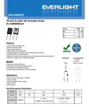
- Repetitive Peak Reverse Voltage (VRRM): 650V. This is the maximum instantaneous reverse voltage that can be applied repetitively. It defines the voltage rating of the device and is crucial for selecting the diode for a given bus voltage, typically with a safety margin.
- Continuous Forward Current (IF): 8A. This is the maximum average forward current the diode can conduct continuously, limited by the maximum junction temperature and thermal resistance. The value of 8A is specified at a case temperature (TC) of 25°C. In real applications, derating based on the actual operating temperature is necessary.
- Forward Voltage (VF): Typically 1.5V at 8A and 25°C junction temperature (TJ), with a maximum of 1.85V. This parameter is critical for calculating conduction losses (P_conduction = VF * IF). The low VF is a key benefit of SiC Schottky technology, directly contributing to higher system efficiency. Note that VF has a negative temperature coefficient, meaning it decreases slightly as temperature increases, which helps prevent thermal runaway in parallel configurations.
- Reverse Current (IR): Typically 2µA at 520V and 25°C TJ. This is the leakage current when the diode is reverse-biased. Low leakage current minimizes off-state power losses.
- Total Capacitive Charge (QC): 12 nC (typical) at VR=400V. This is a critical parameter for high-frequency switching. QC represents the charge associated with the diode's junction capacitance that must be displaced during each switching cycle. A low QC value directly translates to lower switching losses, enabling higher frequency operation.
- Surge Non-Repetitive Forward Current (IFSM): 29A. This is the maximum allowable non-repetitive peak current for a short duration (10ms, half-sine wave). It indicates the device's ability to withstand inrush or fault currents, such as those encountered during startup or load transients.
2.2 Thermal Characteristics
Thermal management is paramount for reliability and performance.
- Maximum Junction Temperature (TJ,max): 175°C. This is the absolute maximum temperature the semiconductor junction can withstand. Continuous operation at or near this limit will significantly reduce the device's lifetime.
- Thermal Resistance, Junction-to-Case (RθJC): 1.9 °C/W (typical). This parameter quantifies the thermal impedance between the semiconductor die (junction) and the exterior case of the package. A lower value indicates better heat transfer from the die to the heatsink. The total junction temperature rise can be calculated as ΔTJ = PD * RθJC, where PD is the power dissipated in the diode.
- Total Power Dissipation (PD): 42W at TC=25°C. This is the maximum power the device can dissipate under the specified test condition. In practice, the allowable dissipation decreases as the case temperature increases.
3. Performance Curve Analysis
The datasheet provides several characteristic curves essential for design and analysis.
3.1 VF-IF Characteristics
This graph plots forward voltage (VF) against forward current (IF). It shows the non-linear relationship, typically starting with a knee voltage and then increasing approximately linearly. Designers use this curve to accurately determine conduction losses at specific operating currents, which is more precise than using a single typical VF value.
3.2 VR-IR Characteristics
This curve illustrates the reverse leakage current (IR) as a function of the applied reverse voltage (VR). It demonstrates how leakage current increases with both reverse voltage and junction temperature. This is vital for estimating off-state losses, especially in high-voltage applications.
3.3 VR-Ct Characteristics
This graph shows the total capacitance (Ct) of the diode versus reverse voltage (VR). The junction capacitance is highly non-linear, decreasing significantly as the reverse voltage increases (from 208 pF at 1V to 18 pF at 400V). This non-linear capacitance is a key factor in calculating the switching behavior and the QC parameter.
3.4 Maximum Forward Current vs. Case Temperature
This derating curve shows how the maximum allowable continuous forward current (IF) decreases as the case temperature (TC) increases. It is a fundamental guide for heatsink design, ensuring the junction temperature does not exceed its maximum rating under all operating conditions.
3.5 Transient Thermal Impedance
This curve plots the transient thermal resistance (ZθJC) against pulse width. It is crucial for evaluating the junction temperature rise during short-duration power pulses, such as those occurring during switching events or surge conditions. The thermal mass of the package causes the effective thermal resistance to be lower for very short pulses.
4. Mechanical and Package Information
4.1 Package Outline and Dimensions
The device uses the industry-standard TO-247-2L package. Key dimensions from the outline drawing include a total package length of approximately 20.0 mm, a width of 16.26 mm, and a height of 4.7 mm (excluding leads). The leads have a specific thickness and spacing to ensure compatibility with standard PCB layouts and heatsink mounting holes.
4.2 Pin Configuration and Polarity Identification
The TO-247-2L package has two leads. Pin 1 is identified as the Cathode (K), and Pin 2 is the Anode (A). Importantly, the metal tab or case of the package is electrically connected to the Cathode. This must be carefully considered during mounting to ensure proper electrical isolation if the heatsink is not at cathode potential. A recommended PCB land pattern (pad layout) is provided to ensure reliable soldering and thermal performance when using a surface-mount lead form.
5. Mounting and Assembly Guidelines
Proper installation is critical for performance and reliability.
- Mounting Torque: The recommended mounting torque for the fixing screw (M3 or 6-32) is 8.8 N·cm (or 8.8 lbf-in). Applying the correct torque ensures optimal thermal contact between the package case and the heatsink without damaging the package.
- Thermal Interface Material (TIM): A suitable thermal grease or pad must always be used between the diode case and the heatsink to fill microscopic air gaps and minimize thermal resistance.
- Electrical Isolation: Since the case is connected to the cathode, an electrically insulating but thermally conductive pad (e.g., mica, silicone rubber with ceramic filler) is required if the heatsink is at a different potential. The isolation voltage rating of this pad must exceed the system's operating voltage.
- Storage Conditions: The device should be stored within a temperature range of -55°C to +175°C in a dry, non-corrosive environment.
6. Application Recommendations
6.1 Typical Application Circuits
This SiC Schottky diode is ideally suited for several key power electronic circuits:
- Power Factor Correction (PFC): Used in the boost converter stage of switched-mode power supplies (SMPS). Its fast switching and low QC reduce switching losses at high frequencies (often 65kHz to 150kHz), improving PFC stage efficiency.
- Solar Inverter DC-AC Stage: Employed in the inverter bridge or as a freewheeling diode. The high voltage rating and efficiency contribute to higher overall inverter efficiency, which is critical for solar energy yield.
- Uninterruptible Power Supply (UPS): Used in both the rectifier/charger and inverter sections. The high surge capability (IFSM) helps handle battery charging currents and output load transients.
- Motor Drive Inverters: Acts as the freewheeling diode across Insulated-Gate Bipolar Transistors (IGBTs) or MOSFETs in the output bridge. The lack of reverse recovery charge eliminates reverse recovery losses and associated voltage spikes, allowing for smoother switching and reduced electromagnetic interference (EMI).
6.2 Design Considerations
- Snubber Circuits: Due to the very fast switching and essentially no reverse recovery, snubber circuits for controlling di/dt or dv/dt may be simplified or even unnecessary compared to silicon PN junction diodes. However, layout-induced parasitic inductance can still cause voltage overshoot and must be minimized with a tight PCB layout.
- Parallel Operation: The negative temperature coefficient of VF makes these diodes inherently suitable for parallel operation to increase current handling. As one diode heats up, its VF decreases, causing it to share more current, which promotes current balancing rather than thermal runaway. However, careful attention to symmetrical layout and thermal coupling is still recommended.
- Heatsink Sizing: Use the power dissipation (calculated from VF and IR), RθJC, and the derating curve to accurately size the heatsink. The goal is to keep the junction temperature well below 175°C (e.g., 125-150°C) for long-term reliability.
7. Technical Comparison and Advantages
Compared to standard silicon fast recovery diodes (FRDs) or even silicon PN diodes, this SiC Schottky diode offers distinct advantages:
- Essentially Zero Reverse Recovery: The Schottky barrier is a majority carrier device, unlike PN junctions which are minority carrier devices. This eliminates the stored charge and the associated reverse recovery time (trr) and current (Irr). This is the single most significant advantage, leading to dramatically lower switching losses.
- Higher Operating Temperature: Silicon Carbide's wider bandgap allows for a higher maximum junction temperature (175°C vs. typically 150°C for silicon), offering more design margin or allowing for smaller heatsinks.
- Higher Switching Frequency: The combination of low QC and no reverse recovery enables efficient operation at much higher frequencies. This allows for the use of smaller passive components (inductors, capacitors, transformers), increasing power density.
- Lower Forward Voltage Drop: At typical operating currents, SiC Schottky diodes often have a comparable or lower VF than high-voltage silicon FRDs, reducing conduction losses.
- Trade-off: The primary historical trade-off was cost, though SiC device prices have decreased significantly. Also, the reverse leakage current of Schottky diodes is generally higher than that of PN diodes and increases more sharply with temperature, which can be a consideration in very high-temperature applications.
8. Frequently Asked Questions (FAQ)
Q1: What does \"essentially no switching losses\" mean in practice?
A1: It means the dominant switching loss mechanism in a diode—the reverse recovery loss—is negligible. However, losses still occur due to the charging and discharging of the junction capacitance (related to QC). These capacitive losses are typically much smaller than the reverse recovery losses of a silicon diode, especially at high frequencies.
Q2: How do I select a heatsink for this diode?
A2: First, calculate the worst-case power dissipation: PD = (VF * IF_avg) + (VR * IR_avg). Use the VF and IR values at your expected operating junction temperature. Then, determine your target maximum junction temperature (e.g., 140°C). The required thermal resistance of the heatsink (RθSA) can be found from: RθSA = (TJ - TA) / PD - RθJC - RθCS, where TA is ambient temperature and RθCS is the thermal resistance of the interface material.
Q3: Can I use this diode directly as a replacement for a silicon diode in my existing circuit?
A3: Not always without review. While the pinout and package may be compatible, the faster switching can lead to higher voltage spikes due to circuit parasitic inductance. The gate drive or control for the associated switching transistor might need adjustment. The lower forward voltage may also slightly change circuit behavior. A thorough design review is recommended.
Q4: Why is the case connected to the cathode?
A4: This is common in power packages. It allows the large metal tab, which is excellent for heat transfer, to be used as an electrical connection. This reduces the parasitic inductance in the cathode path, which is beneficial for high-speed switching. It necessitates careful isolation if the heatsink is not at cathode potential.
9. Practical Design Case Study
Scenario: Designing a 1.5kW Boost PFC Stage.
Assume an input voltage range of 85-265VAC, output voltage of 400VDC, and switching frequency of 100kHz. The boost diode must block 400V and carry the inductor current. Calculations show a peak current of around 10A and an average diode current of approximately 4A.
A silicon ultrafast diode with a trr of 50ns and QC of 30nC would incur significant reverse recovery losses at 100kHz. By selecting this SiC Schottky diode (QC=12nC, no trr), the switching losses in the diode are reduced to only the capacitive losses. This directly improves efficiency by 0.5-1.5%, reduces heat generation, and may allow for a smaller heatsink or enable operation at a higher ambient temperature. The design also benefits from reduced EMI due to the absence of reverse recovery current spikes.
10. Operating Principle
A Schottky diode is formed by a metal-semiconductor junction, unlike a standard PN junction diode which uses a semiconductor-semiconductor junction. In a SiC Schottky diode, a metal (e.g., Titanium) is deposited on Silicon Carbide. This creates a Schottky barrier which allows current to flow freely in the forward direction when a small voltage is applied (the low VF). In the reverse direction, the barrier blocks current flow. Because conduction relies only on majority carriers (electrons in an N-type SiC substrate), there is no injection and storage of minority carriers. Consequently, when the voltage reverses, there is no stored charge to be removed, resulting in the near-instantaneous turn-off characteristic and the absence of reverse recovery.
11. Technology Trends
Silicon Carbide power devices, including Schottky diodes and MOSFETs, represent a major trend in power electronics towards higher efficiency, frequency, and power density. The market is moving from 600-650V devices (competing with silicon Superjunction MOSFETs and IGBTs) to 1200V and 1700V ratings for industrial and automotive applications. The integration of SiC diodes with SiC MOSFETs in modules is becoming common for complete high-performance power stages. Continuous improvements in SiC material quality and fabrication processes are driving down costs and improving device reliability, making SiC technology the preferred choice for new designs in medium and high-power applications where performance is critical.
LED Specification Terminology
Complete explanation of LED technical terms
Photoelectric Performance
| Term | Unit/Representation | Simple Explanation | Why Important |
|---|---|---|---|
| Luminous Efficacy | lm/W (lumens per watt) | Light output per watt of electricity, higher means more energy efficient. | Directly determines energy efficiency grade and electricity cost. |
| Luminous Flux | lm (lumens) | Total light emitted by source, commonly called "brightness". | Determines if the light is bright enough. |
| Viewing Angle | ° (degrees), e.g., 120° | Angle where light intensity drops to half, determines beam width. | Affects illumination range and uniformity. |
| CCT (Color Temperature) | K (Kelvin), e.g., 2700K/6500K | Warmth/coolness of light, lower values yellowish/warm, higher whitish/cool. | Determines lighting atmosphere and suitable scenarios. |
| CRI / Ra | Unitless, 0–100 | Ability to render object colors accurately, Ra≥80 is good. | Affects color authenticity, used in high-demand places like malls, museums. |
| SDCM | MacAdam ellipse steps, e.g., "5-step" | Color consistency metric, smaller steps mean more consistent color. | Ensures uniform color across same batch of LEDs. |
| Dominant Wavelength | nm (nanometers), e.g., 620nm (red) | Wavelength corresponding to color of colored LEDs. | Determines hue of red, yellow, green monochrome LEDs. |
| Spectral Distribution | Wavelength vs intensity curve | Shows intensity distribution across wavelengths. | Affects color rendering and quality. |
Electrical Parameters
| Term | Symbol | Simple Explanation | Design Considerations |
|---|---|---|---|
| Forward Voltage | Vf | Minimum voltage to turn on LED, like "starting threshold". | Driver voltage must be ≥Vf, voltages add up for series LEDs. |
| Forward Current | If | Current value for normal LED operation. | Usually constant current drive, current determines brightness & lifespan. |
| Max Pulse Current | Ifp | Peak current tolerable for short periods, used for dimming or flashing. | Pulse width & duty cycle must be strictly controlled to avoid damage. |
| Reverse Voltage | Vr | Max reverse voltage LED can withstand, beyond may cause breakdown. | Circuit must prevent reverse connection or voltage spikes. |
| Thermal Resistance | Rth (°C/W) | Resistance to heat transfer from chip to solder, lower is better. | High thermal resistance requires stronger heat dissipation. |
| ESD Immunity | V (HBM), e.g., 1000V | Ability to withstand electrostatic discharge, higher means less vulnerable. | Anti-static measures needed in production, especially for sensitive LEDs. |
Thermal Management & Reliability
| Term | Key Metric | Simple Explanation | Impact |
|---|---|---|---|
| Junction Temperature | Tj (°C) | Actual operating temperature inside LED chip. | Every 10°C reduction may double lifespan; too high causes light decay, color shift. |
| Lumen Depreciation | L70 / L80 (hours) | Time for brightness to drop to 70% or 80% of initial. | Directly defines LED "service life". |
| Lumen Maintenance | % (e.g., 70%) | Percentage of brightness retained after time. | Indicates brightness retention over long-term use. |
| Color Shift | Δu′v′ or MacAdam ellipse | Degree of color change during use. | Affects color consistency in lighting scenes. |
| Thermal Aging | Material degradation | Deterioration due to long-term high temperature. | May cause brightness drop, color change, or open-circuit failure. |
Packaging & Materials
| Term | Common Types | Simple Explanation | Features & Applications |
|---|---|---|---|
| Package Type | EMC, PPA, Ceramic | Housing material protecting chip, providing optical/thermal interface. | EMC: good heat resistance, low cost; Ceramic: better heat dissipation, longer life. |
| Chip Structure | Front, Flip Chip | Chip electrode arrangement. | Flip chip: better heat dissipation, higher efficacy, for high-power. |
| Phosphor Coating | YAG, Silicate, Nitride | Covers blue chip, converts some to yellow/red, mixes to white. | Different phosphors affect efficacy, CCT, and CRI. |
| Lens/Optics | Flat, Microlens, TIR | Optical structure on surface controlling light distribution. | Determines viewing angle and light distribution curve. |
Quality Control & Binning
| Term | Binning Content | Simple Explanation | Purpose |
|---|---|---|---|
| Luminous Flux Bin | Code e.g., 2G, 2H | Grouped by brightness, each group has min/max lumen values. | Ensures uniform brightness in same batch. |
| Voltage Bin | Code e.g., 6W, 6X | Grouped by forward voltage range. | Facilitates driver matching, improves system efficiency. |
| Color Bin | 5-step MacAdam ellipse | Grouped by color coordinates, ensuring tight range. | Guarantees color consistency, avoids uneven color within fixture. |
| CCT Bin | 2700K, 3000K etc. | Grouped by CCT, each has corresponding coordinate range. | Meets different scene CCT requirements. |
Testing & Certification
| Term | Standard/Test | Simple Explanation | Significance |
|---|---|---|---|
| LM-80 | Lumen maintenance test | Long-term lighting at constant temperature, recording brightness decay. | Used to estimate LED life (with TM-21). |
| TM-21 | Life estimation standard | Estimates life under actual conditions based on LM-80 data. | Provides scientific life prediction. |
| IESNA | Illuminating Engineering Society | Covers optical, electrical, thermal test methods. | Industry-recognized test basis. |
| RoHS / REACH | Environmental certification | Ensures no harmful substances (lead, mercury). | Market access requirement internationally. |
| ENERGY STAR / DLC | Energy efficiency certification | Energy efficiency and performance certification for lighting. | Used in government procurement, subsidy programs, enhances competitiveness. |