Table of Contents
- 1. Product Overview
- 1.1 Core Advantages and Target Market
- 2. In-Depth Technical Parameter Analysis
- 2.1 Absolute Maximum Ratings
- 2.2 Electrical Characteristics
- 2.3 Thermal Characteristics
- 3. Performance Curve Analysis
- 3.1 VF-IF Characteristics
- 3.2 Maximum Forward Current vs. Case Temperature
- 3.3 Transient Thermal Impedance
- 4. Mechanical and Package Information
- 4.1 Pin Configuration and Polarity
- 4.2 Package Dimensions and Mounting
- 5. Application Guidelines and Design Considerations
- 5.1 Typical Application Circuits
- 5.2 Thermal Design and Heat Sinking
- 5.3 Parallel Operation
- 6. Technical Comparison and Differentiation
- 7. Frequently Asked Questions (Based on Technical Parameters)
- 7.1 What does "essentially no switching losses" mean?
- 7.2 How does the low Qc enable higher frequency operation?
- 7.3 Why is the case connected to the cathode, and what are the implications?
- 8. Practical Design Case Study
- 9. Operating Principle
- 10. Technology Trends
1. Product Overview
This document details the specifications for a high-performance Silicon Carbide (SiC) Schottky Barrier Diode (SBD) housed in a TO-247-2L package. The device is engineered for power conversion applications requiring high efficiency, high-frequency operation, and robust thermal performance. Its core function is to provide unidirectional current flow with minimal switching losses and reverse recovery charge, a significant advantage over traditional silicon PN-junction diodes.
1.1 Core Advantages and Target Market
The primary advantages of this SiC Schottky diode stem from the material properties of Silicon Carbide. Key benefits include a low forward voltage drop (VF), which reduces conduction losses, and an inherently fast switching capability with essentially no reverse recovery charge (Qc). This enables operation at higher frequencies, leading to smaller passive components (inductors, capacitors) and overall system size reduction. The high maximum junction temperature (TJ,max) of 175°C allows for operation in demanding thermal environments or permits the use of smaller heat sinks. These characteristics make it ideal for modern, high-density power supplies. The target applications are clearly defined as Power Factor Correction (PFC) circuits in Switch-Mode Power Supplies (SMPS), solar inverters, Uninterruptible Power Supplies (UPS), motor drives, and data center power infrastructure, where efficiency and power density are critical parameters.
2. In-Depth Technical Parameter Analysis
The datasheet provides comprehensive electrical and thermal ratings essential for reliable circuit design. Understanding these parameters is crucial for ensuring the device operates within its safe operating area (SOA).
2.1 Absolute Maximum Ratings
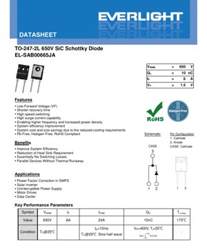
These ratings define the stress limits beyond which permanent damage to the device may occur. They are not intended for normal operation. Key ratings include: Repetitive Peak Reverse Voltage (VRRM) and DC Blocking Voltage (VR) of 650V, defining the maximum allowable reverse bias. The Continuous Forward Current (IF) is rated at 6A, limited by the maximum junction temperature and thermal resistance. A significant parameter is the non-repetitive surge current (IFSM) of 24A for a 10ms half-sine wave, indicating robustness against short-duration overloads. The maximum junction temperature (TJ) is 175°C, and the total power dissipation (PD) is specified as 71W at a case temperature (TC) of 25°C, though this is highly dependent on thermal management.
2.2 Electrical Characteristics
This section details the typical and maximum performance values under specified test conditions. The forward voltage (VF) is a critical parameter for conduction loss calculation; it is typically 1.5V at 6A and 25°C, increasing to a maximum of 1.9V at the high junction temperature of 175°C. The reverse leakage current (IR) is very low, typically 0.8µA at 520V and 25°C, showcasing the excellent blocking capability of the SiC Schottky junction. Perhaps the most defining feature is the total capacitive charge (QC), specified as 10nC at 400V. This extremely low value confirms the near-zero reverse recovery behavior, which is the source of the diode's high-speed switching performance and low switching losses. The capacitance stored energy (EC) is correspondingly low at 1.5µJ.
2.3 Thermal Characteristics
Effective thermal management is paramount for reliability. The key parameter here is the Thermal Resistance from Junction to Case (Rth(JC)), with a typical value of 2.1°C/W. This low value indicates efficient heat transfer from the semiconductor die to the device case, which must then be dissipated via a heat sink. The thermal resistance value is used in conjunction with power dissipation and ambient/case temperature to calculate the actual junction temperature using the formula: TJ = TC + (PD * Rth(JC)). Ensuring TJ remains below 175°C is essential for long-term reliability.
3. Performance Curve Analysis
Graphical data provides insight into device behavior under various operating conditions, complementing the tabular data.
3.1 VF-IF Characteristics
The forward voltage versus forward current curve illustrates the diode's conduction behavior. It typically shows an exponential relationship at very low currents, transitioning to a more linear relationship dominated by the series resistance at higher currents like the rated 6A. The positive temperature coefficient of VF (it increases with temperature) is a beneficial trait for parallel operation, as it promotes current sharing and prevents thermal runaway.
3.2 Maximum Forward Current vs. Case Temperature
This derating curve shows how the maximum allowable continuous forward current (IF) decreases as the case temperature (TC) increases. Designers must use this graph to determine the safe operating current for their specific thermal environment. At the maximum case temperature (which will be lower than TJ,max), the allowable current may be significantly less than the 6A rated at 25°C.
3.3 Transient Thermal Impedance
The curve of transient thermal resistance versus pulse width is vital for evaluating thermal performance under pulsed loading conditions, common in switching applications. It shows that for very short pulses, the effective thermal resistance from junction to case is lower than the steady-state Rth(JC), meaning the junction temperature rise for a single short pulse is less than for continuous dissipation of the same power. This data is used for loss analysis in switching converters.
4. Mechanical and Package Information
4.1 Pin Configuration and Polarity
The device uses a TO-247-2L package with two leads. Pin 1 is identified as the Cathode (K), and Pin 2 is the Anode (A). Importantly, the metal tab or case of the package is also connected to the Cathode. This must be carefully considered during mounting, as the tab typically requires electrical isolation from the heat sink (using an insulating washer) unless the heat sink is at cathode potential.
4.2 Package Dimensions and Mounting
The datasheet includes detailed mechanical drawings with dimensions in millimeters for the TO-247-2L package. It also provides a recommended pad layout for a surface-mount lead form, which is useful for PCB design if the leads are formed for surface mounting. The maximum mounting torque for the screw used to attach the device to a heat sink is specified as 8.8 Nm (or equivalent in lbf-in) for an M3 or 6-32 screw. Applying the correct torque is critical for ensuring good thermal contact without damaging the package.
5. Application Guidelines and Design Considerations
5.1 Typical Application Circuits
The primary application highlighted is Power Factor Correction (PFC), particularly in boost converter topologies. In a PFC boost circuit, the diode carries the inductor current when the main switch is off. The fast switching and low Qc of this SiC diode minimize turn-off losses associated with reverse recovery, allowing for higher switching frequencies. This leads to smaller magnetic components (the boost inductor) and improved power density. Other applications like solar inverters and UPS systems benefit similarly in their DC-link or output rectification stages.
5.2 Thermal Design and Heat Sinking
A critical design task is selecting an appropriate heat sink. The process involves: 1) Calculating total power dissipation in the diode (conduction loss + switching loss, though switching loss is minimal). 2) Determining the maximum allowable case temperature based on the ambient temperature, required safety margin, and the junction-to-case thermal resistance. 3) Using this to calculate the required thermal resistance of the heat sink (Rth(SA)). The formula is: Rth(SA) = (TC - TA) / PD - Rth(JC) - Rth(CS), where Rth(CS) is the thermal resistance of the interface material (thermal grease/pad). The low Qc directly reduces switching losses, which in turn reduces the heat sink requirement, enabling cost and size savings as stated in the features.
5.3 Parallel Operation
The positive temperature coefficient of VF facilitates safe parallel operation of multiple devices for higher current capability. As one diode heats up and its VF increases, current naturally shifts to the cooler parallel device, promoting balanced current sharing. This is a significant advantage over some diodes with negative temperature coefficients that can suffer from thermal runaway in parallel configurations.
6. Technical Comparison and Differentiation
Compared to standard silicon fast-recovery diodes (FRDs) or even ultrafast recovery diodes, this SiC Schottky diode offers fundamental advantages. Silicon diodes have a substantial reverse recovery charge (Qrr), leading to significant switching losses, voltage spikes, and electromagnetic interference (EMI) at turn-off. The SiC Schottky diode's Qc is orders of magnitude lower, virtually eliminating these issues. While silicon carbide Schottky diodes historically had higher forward voltage drops than silicon PN diodes, modern devices like this one have achieved competitive VF values (1.5V) while retaining the switching benefits. The higher maximum operating temperature (175°C vs. typically 150°C for silicon) also provides a reliability margin in high-temperature environments.
7. Frequently Asked Questions (Based on Technical Parameters)
7.1 What does "essentially no switching losses" mean?
This refers to the near-absence of reverse recovery loss. In a switching circuit, when a diode is switched from forward conduction to reverse blocking, stored charge in a conventional diode must be removed, causing a reverse current pulse and associated energy loss. The SiC Schottky diode's Qc of only 10nC means this charge is minuscule, making the switching loss negligible compared to conduction loss.
7.2 How does the low Qc enable higher frequency operation?
Switching losses are proportional to switching frequency. With traditional diodes, high reverse recovery loss limits the maximum practical switching frequency due to excessive heat generation. Since the SiC diode's switching loss is minimal, the frequency can be increased significantly. Higher frequency allows the use of smaller inductors and transformers, directly increasing power density.
7.3 Why is the case connected to the cathode, and what are the implications?
This is a common design in power packages for electrical and thermal reasons. It means the metal tab, which is the primary thermal path, is electrically live (at cathode potential). Therefore, if multiple devices on different potentials are mounted on a common heat sink, insulating hardware (mica washers, silicone pads, etc.) must be used to prevent short circuits. The thermal interface material must also have good dielectric strength.
8. Practical Design Case Study
Consider designing a 1kW, 80kHz boost PFC stage with an output voltage of 400VDC. A silicon ultrafast diode might have a Qrr of 50nC. The reverse recovery loss per cycle can be estimated as 0.5 * Vout * Qrr * fsw. This would be 0.5 * 400V * 50nC * 80kHz = 0.8W. Using the SiC Schottky diode with Qc=10nC reduces this loss to 0.5 * 400V * 10nC * 80kHz = 0.16W, a saving of 0.64W. This reduced loss lowers the junction temperature or allows for a smaller heat sink. Furthermore, the absence of reverse recovery current reduces stress on the main switch (MOSFET/IGBT) and minimizes EMI, potentially simplifying the input filter design.
9. Operating Principle
A Schottky diode is formed by a metal-semiconductor junction, unlike a PN junction diode. In a Silicon Carbide Schottky diode, the metal contact is made to a wide-bandgap SiC semiconductor. This structure results in a lower forward voltage drop for a given current density compared to a PN junction and, crucially, has no minority carrier storage. Therefore, when the voltage reverses, there is no slow process of minority carrier recombination to cause a reverse recovery current; the junction capacitance simply discharges. This is the fundamental reason for its fast switching speed and low Qc.
10. Technology Trends
Silicon Carbide power devices, including Schottky diodes and MOSFETs, are a key enabling technology for modern high-efficiency power electronics. The trend is towards higher voltage ratings (e.g., 1200V, 1700V) for applications like electric vehicle traction inverters and industrial drives, lower specific on-resistance for MOSFETs, and improved reliability. Integration is also a trend, with the emergence of power modules combining SiC MOSFETs and Schottky diodes in half-bridge or other configurations. As manufacturing volumes increase and costs decrease, SiC technology is progressively displacing silicon IGBTs and diodes in medium-power applications where efficiency, frequency, and power density are driving factors.
LED Specification Terminology
Complete explanation of LED technical terms
Photoelectric Performance
| Term | Unit/Representation | Simple Explanation | Why Important |
|---|---|---|---|
| Luminous Efficacy | lm/W (lumens per watt) | Light output per watt of electricity, higher means more energy efficient. | Directly determines energy efficiency grade and electricity cost. |
| Luminous Flux | lm (lumens) | Total light emitted by source, commonly called "brightness". | Determines if the light is bright enough. |
| Viewing Angle | ° (degrees), e.g., 120° | Angle where light intensity drops to half, determines beam width. | Affects illumination range and uniformity. |
| CCT (Color Temperature) | K (Kelvin), e.g., 2700K/6500K | Warmth/coolness of light, lower values yellowish/warm, higher whitish/cool. | Determines lighting atmosphere and suitable scenarios. |
| CRI / Ra | Unitless, 0–100 | Ability to render object colors accurately, Ra≥80 is good. | Affects color authenticity, used in high-demand places like malls, museums. |
| SDCM | MacAdam ellipse steps, e.g., "5-step" | Color consistency metric, smaller steps mean more consistent color. | Ensures uniform color across same batch of LEDs. |
| Dominant Wavelength | nm (nanometers), e.g., 620nm (red) | Wavelength corresponding to color of colored LEDs. | Determines hue of red, yellow, green monochrome LEDs. |
| Spectral Distribution | Wavelength vs intensity curve | Shows intensity distribution across wavelengths. | Affects color rendering and quality. |
Electrical Parameters
| Term | Symbol | Simple Explanation | Design Considerations |
|---|---|---|---|
| Forward Voltage | Vf | Minimum voltage to turn on LED, like "starting threshold". | Driver voltage must be ≥Vf, voltages add up for series LEDs. |
| Forward Current | If | Current value for normal LED operation. | Usually constant current drive, current determines brightness & lifespan. |
| Max Pulse Current | Ifp | Peak current tolerable for short periods, used for dimming or flashing. | Pulse width & duty cycle must be strictly controlled to avoid damage. |
| Reverse Voltage | Vr | Max reverse voltage LED can withstand, beyond may cause breakdown. | Circuit must prevent reverse connection or voltage spikes. |
| Thermal Resistance | Rth (°C/W) | Resistance to heat transfer from chip to solder, lower is better. | High thermal resistance requires stronger heat dissipation. |
| ESD Immunity | V (HBM), e.g., 1000V | Ability to withstand electrostatic discharge, higher means less vulnerable. | Anti-static measures needed in production, especially for sensitive LEDs. |
Thermal Management & Reliability
| Term | Key Metric | Simple Explanation | Impact |
|---|---|---|---|
| Junction Temperature | Tj (°C) | Actual operating temperature inside LED chip. | Every 10°C reduction may double lifespan; too high causes light decay, color shift. |
| Lumen Depreciation | L70 / L80 (hours) | Time for brightness to drop to 70% or 80% of initial. | Directly defines LED "service life". |
| Lumen Maintenance | % (e.g., 70%) | Percentage of brightness retained after time. | Indicates brightness retention over long-term use. |
| Color Shift | Δu′v′ or MacAdam ellipse | Degree of color change during use. | Affects color consistency in lighting scenes. |
| Thermal Aging | Material degradation | Deterioration due to long-term high temperature. | May cause brightness drop, color change, or open-circuit failure. |
Packaging & Materials
| Term | Common Types | Simple Explanation | Features & Applications |
|---|---|---|---|
| Package Type | EMC, PPA, Ceramic | Housing material protecting chip, providing optical/thermal interface. | EMC: good heat resistance, low cost; Ceramic: better heat dissipation, longer life. |
| Chip Structure | Front, Flip Chip | Chip electrode arrangement. | Flip chip: better heat dissipation, higher efficacy, for high-power. |
| Phosphor Coating | YAG, Silicate, Nitride | Covers blue chip, converts some to yellow/red, mixes to white. | Different phosphors affect efficacy, CCT, and CRI. |
| Lens/Optics | Flat, Microlens, TIR | Optical structure on surface controlling light distribution. | Determines viewing angle and light distribution curve. |
Quality Control & Binning
| Term | Binning Content | Simple Explanation | Purpose |
|---|---|---|---|
| Luminous Flux Bin | Code e.g., 2G, 2H | Grouped by brightness, each group has min/max lumen values. | Ensures uniform brightness in same batch. |
| Voltage Bin | Code e.g., 6W, 6X | Grouped by forward voltage range. | Facilitates driver matching, improves system efficiency. |
| Color Bin | 5-step MacAdam ellipse | Grouped by color coordinates, ensuring tight range. | Guarantees color consistency, avoids uneven color within fixture. |
| CCT Bin | 2700K, 3000K etc. | Grouped by CCT, each has corresponding coordinate range. | Meets different scene CCT requirements. |
Testing & Certification
| Term | Standard/Test | Simple Explanation | Significance |
|---|---|---|---|
| LM-80 | Lumen maintenance test | Long-term lighting at constant temperature, recording brightness decay. | Used to estimate LED life (with TM-21). |
| TM-21 | Life estimation standard | Estimates life under actual conditions based on LM-80 data. | Provides scientific life prediction. |
| IESNA | Illuminating Engineering Society | Covers optical, electrical, thermal test methods. | Industry-recognized test basis. |
| RoHS / REACH | Environmental certification | Ensures no harmful substances (lead, mercury). | Market access requirement internationally. |
| ENERGY STAR / DLC | Energy efficiency certification | Energy efficiency and performance certification for lighting. | Used in government procurement, subsidy programs, enhances competitiveness. |