Table of Contents
- 1. Product Overview
- 2. In-Depth Technical Parameter Analysis
- 2.1 Electrical Characteristics
- 2.2 Thermal Characteristics
- 2.3 Maximum Ratings and Absolute Limits
- 3. Performance Curve Analysis
- 3.1 VF-IF Characteristics
- 3.2 VR-IR Characteristics
- 3.3 Maximum Forward Current vs. Case Temperature
- 3.4 Transient Thermal Impedance
- 4. Mechanical and Package Information
- 4.1 Package Dimensions (TO-247-2L)
- 4.2 Pin Configuration and Polarity
- 4.3 Recommended PCB Land Pattern
- 5. Application Guidelines
- 5.1 Typical Application Circuits
- 5.2 Design Considerations and Best Practices
- 6. Technical Comparison and Advantages
- 7. Frequently Asked Questions (FAQs)
- 7.1 Can this diode be used as a replacement for a silicon diode in an existing design?
- 7.2 Why is the forward voltage (1.4V) higher than a typical silicon Schottky diode?
- 7.3 How do I parallel these diodes for higher current?
- 7.4 What is the significance of the "Total Capacitive Charge (QC)" parameter?
- 8. Industry Trends and Future Developments
1. Product Overview
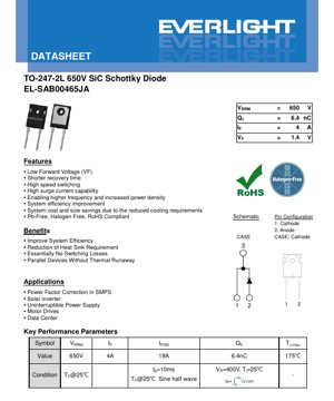
This document details the specifications for a high-performance Silicon Carbide (SiC) Schottky Barrier Diode (SBD) housed in a TO-247-2L package. The device is engineered for high-voltage, high-frequency power conversion applications where efficiency, thermal management, and switching speed are critical. Utilizing SiC technology, this diode offers significant advantages over traditional silicon-based counterparts, particularly in reducing switching losses and enabling higher operating frequencies.
The core function of this component is to provide unidirectional current flow with minimal voltage drop and near-zero reverse recovery charge. Its primary role is in circuits requiring fast switching and high efficiency, such as switch-mode power supplies (SMPS), inverters, and motor drives. The fundamental operating principle relies on the metal-semiconductor junction of a Schottky barrier, which, when fabricated with Silicon Carbide, allows for a high breakdown voltage while maintaining a low forward voltage drop and excellent high-temperature performance.
2. In-Depth Technical Parameter Analysis
2.1 Electrical Characteristics
The electrical parameters define the operational boundaries and performance of the diode under various conditions.
- Maximum Repetitive Peak Reverse Voltage (VRRM): 650V. This is the maximum instantaneous reverse voltage the diode can withstand repeatedly. It defines the voltage rating for the device in applications like power factor correction (PFC) stages operating from a rectified 230VAC mains.
- Continuous Forward Current (IF): 4A. This is the maximum average forward current the diode can conduct continuously, limited by its thermal characteristics. The actual usable current depends on the heatsinking and ambient temperature.
- Forward Voltage (VF): Typically 1.4V at IF=4A and TJ=25°C, with a maximum of 1.75V. This parameter is crucial for calculating conduction losses (Pcond = VF * IF). The low VF is a key benefit of SiC Schottky technology, directly contributing to higher system efficiency.
- Reverse Leakage Current (IR): Maximum 25 µA at VR=520V and TJ=25°C. This low leakage current minimizes off-state power losses.
- Total Capacitive Charge (QC): 6.4 nC (typical) at VR=400V. This is a critical parameter for high-frequency switching. A low QC value indicates that very little charge needs to be displaced during each switching cycle, resulting in significantly lower switching losses compared to silicon PN junction diodes or even silicon carbide MOSFET body diodes.
- Capacitance Stored Energy (EC): 1 µJ (typical) at VR=400V. This energy is dissipated during each turn-on event and is part of the total switching loss calculation.
2.2 Thermal Characteristics
Thermal management is paramount for reliable operation and achieving rated performance.
- Maximum Junction Temperature (TJ,max): 175°C. This is the absolute maximum temperature the semiconductor junction can reach. Operating near this limit will reduce lifetime and reliability.
- Thermal Resistance, Junction-to-Case (RθJC): 4.5 °C/W (typical). This low thermal resistance indicates efficient heat transfer from the silicon die to the package case. It is a fixed property of the device. The total thermal resistance from junction to ambient (RθJA) is the sum of RθJC, the thermal interface material resistance, and the heatsink resistance. A low RθJC allows for smaller heatsinks or higher power dissipation.
- Total Power Dissipation (PD): 33 W at TC=25°C. This rating is derived from the thermal resistance and maximum junction temperature. In practice, the allowable power dissipation decreases as the case temperature rises.
2.3 Maximum Ratings and Absolute Limits
These are stress limits that must not be exceeded under any condition to prevent permanent damage.
- Surge Non-Repetitive Forward Current (IFSM): 19A for a 10ms sine half-wave at TC=25°C. This rating defines the diode's ability to handle short-term overloads, such as inrush currents during power-up.
- Storage Temperature (TSTG): -55°C to +175°C.
- Mounting Torque: 0.8 to 8.8 N·m for an M3 or 6-32 screw. Proper torque ensures good thermal contact between the package tab and the heatsink.
3. Performance Curve Analysis
The datasheet includes several characteristic graphs essential for detailed design.
3.1 VF-IF Characteristics
This graph shows the relationship between forward voltage drop and forward current at different junction temperatures. Key observations: VF has a negative temperature coefficient; it decreases slightly as temperature increases. This characteristic helps prevent thermal runaway when multiple devices are paralleled, as a hotter device will conduct slightly more current, promoting current sharing.
3.2 VR-IR Characteristics
This curve plots reverse leakage current against reverse voltage at different temperatures. It shows that leakage current increases exponentially with both voltage and temperature. Designers must ensure the operating reverse voltage provides sufficient margin below VRRM, especially at high ambient temperatures.
3.3 Maximum Forward Current vs. Case Temperature
This derating curve shows how the maximum allowable continuous forward current decreases as the case temperature increases. It is a direct application of the thermal resistance and maximum junction temperature. For example, to run at the full 4A, the case temperature must be kept at or below 25°C, which typically requires active cooling.
3.4 Transient Thermal Impedance
This graph is vital for evaluating thermal performance during pulsed operation. It shows that for very short pulse widths (e.g., less than 1ms), the effective thermal impedance from junction to case is much lower than the steady-state RθJC. This allows the device to handle higher peak power in switching applications where the duty cycle is low.
4. Mechanical and Package Information
4.1 Package Dimensions (TO-247-2L)
The device uses a standard TO-247-2L package with two leads. Key dimensions include:
- Overall length (D): 15.6 mm (typ)
- Overall width (E): 9.99 mm (typ)
- Overall height (A): 4.5 mm (typ)
- Lead spacing (e1): 5.08 mm (basic)
- Mounting hole distance (E3): 8.70 mm (reference)
The package features an isolated mounting hole, meaning the metal tab (case) is electrically connected to the cathode. This must be considered during heatsink design and electrical isolation.
4.2 Pin Configuration and Polarity
The pinout is clearly defined:
- Pin 1: Cathode (K)
- Pin 2: Anode (A)
- Case (Metal Tab): Connected to Cathode (K)
Correct polarity is essential. Reverse biasing the diode during assembly will cause immediate failure upon power application.
4.3 Recommended PCB Land Pattern
A suggested footprint for surface-mounting the leads is provided, including pad dimensions and spacing to ensure proper solder joint formation and mechanical stability.
5. Application Guidelines
5.1 Typical Application Circuits
This diode is ideally suited for several key power electronic topologies:
- Power Factor Correction (PFC): Used as the boost diode in continuous conduction mode (CCM) or transition mode (TM) PFC circuits. Its fast switching and low QC minimize losses at high switching frequencies (e.g., 65-100 kHz), improving overall power supply efficiency.
- Solar Inverters: Employed in the DC-link or as freewheeling diodes in inverter bridges. The high temperature capability and efficiency are critical for maximizing energy harvest and reliability in outdoor environments.
- Uninterruptible Power Supplies (UPS): Used in the rectifier and inverter stages to improve efficiency and power density.
- Motor Drives: Acts as a freewheeling or clamp diode in IGBT or MOSFET bridges, enabling faster switching and reducing voltage spikes.
- Data Center Power Supplies: High efficiency directly translates to lower operating costs and reduced cooling requirements in high-density server environments.
5.2 Design Considerations and Best Practices
- Thermal Design: Always calculate the required heatsink based on worst-case power dissipation (Pcond + Psw) and maximum ambient temperature. Use thermal interface material (TIM) with low thermal resistance. The mounting torque must be within the specified range.
- Switching Loss Calculation: While the reverse recovery loss is negligible, the capacitive switching loss (Psw_cap = 0.5 * C * V^2 * f) must be calculated using the C-V characteristics and the actual switching frequency and voltage.
- Paralleling Devices: The negative temperature coefficient of VF facilitates current sharing. However, for optimal balance, ensure symmetrical PCB layout, equal length traces/leads, and common heatsinking.
- Voltage Stresses: Include snubber circuits or RC dampers if necessary to control voltage overshoot caused by parasitic inductance in the circuit loop, especially when switching at high di/dt rates.
- Gate Drive Considerations (for associated switches): The fast switching of this diode can cause high dv/dt which may couple into gate drive circuits. Proper layout and shielding are important.
6. Technical Comparison and Advantages
Compared to standard silicon fast recovery diodes (FRDs) or even silicon PN diodes, this SiC Schottky diode offers distinct advantages:
- Essentially Zero Reverse Recovery: The Schottky barrier mechanism has no minority carrier storage, eliminating reverse recovery current (Qrr) and associated switching losses. This is its most significant advantage.
- Higher Operating Temperature: SiC material can operate reliably at junction temperatures up to 175°C, compared to 150°C or lower for many silicon devices.
- Higher Switching Frequency: The absence of Qrr and low QC allow operation at frequencies well above 100 kHz, enabling smaller magnetic components (inductors, transformers) and increased power density.
- Improved System Efficiency: Lower conduction losses (from low VF) and near-zero switching losses directly boost converter efficiency across the load range.
- Reduced Cooling Requirements: Higher efficiency and better high-temperature performance can lead to smaller, lower-cost heatsinks or even passive cooling in some applications.
7. Frequently Asked Questions (FAQs)
7.1 Can this diode be used as a replacement for a silicon diode in an existing design?
While electrically it may function, a direct replacement is not always straightforward. The faster switching can lead to increased electromagnetic interference (EMI) due to higher dv/dt and di/dt. The layout and snubber networks may need re-evaluation. Furthermore, the gate drive of the accompanying switching device (e.g., MOSFET) might be affected by the reduced switching losses and different voltage/current waveforms.
7.2 Why is the forward voltage (1.4V) higher than a typical silicon Schottky diode?
Silicon Schottky diodes have lower barrier heights, leading to VF values around 0.3-0.7V, but their breakdown voltage is typically limited to below 200V. The higher bandgap of Silicon Carbide allows for much higher breakdown voltages (650V in this case) but results in a higher built-in potential and thus a higher forward voltage drop. This is a fundamental trade-off in the material physics.
7.3 How do I parallel these diodes for higher current?
The negative temperature coefficient aids in current sharing. For best results: 1) Mount devices on a common heatsink to equalize case temperatures. 2) Ensure symmetrical PCB layout with identical trace lengths and impedances to each anode and cathode. 3) Consider adding small series resistors or magnetic coupling for forced sharing in critical applications, though often this is not necessary due to the VF characteristic.
7.4 What is the significance of the "Total Capacitive Charge (QC)" parameter?
QC represents the total charge associated with the diode's junction capacitance when charged to a specific voltage (400V here). During turn-on of the opposing switch in a circuit (e.g., a MOSFET in a boost converter), this charge is effectively shorted through the switch, causing a current spike and energy loss. A low QC (6.4nC) means this loss is very small, contributing to the diode's high-speed switching capability.
8. Industry Trends and Future Developments
Silicon Carbide power devices, including Schottky diodes and MOSFETs, are a rapidly growing segment in the power electronics industry. The trend is driven by the global push for higher energy efficiency, compact power supplies, and the electrification of transportation (EVs). Key developments include:
- Higher Voltage Ratings: Devices rated at 1200V and 1700V are becoming more common, targeting applications like electric vehicle traction inverters and industrial motor drives.
- Lower RθJC and Improved Packages: New package technologies (e.g., direct bond copper, improved die attach) are reducing thermal resistance, allowing higher power density.
- Integration: There is a trend towards co-packaging SiC Schottky diodes with SiC MOSFETs in modules to create optimized switching cells with minimal parasitic inductance.
- Cost Reduction: As wafer manufacturing scales and defect densities decrease, the cost premium of SiC over silicon is steadily reducing, broadening its adoption beyond premium applications.
The device described in this datasheet represents a mature and widely adopted point in this technology curve, offering a compelling balance of performance, reliability, and cost for a broad range of high-efficiency power conversion tasks.
LED Specification Terminology
Complete explanation of LED technical terms
Photoelectric Performance
| Term | Unit/Representation | Simple Explanation | Why Important |
|---|---|---|---|
| Luminous Efficacy | lm/W (lumens per watt) | Light output per watt of electricity, higher means more energy efficient. | Directly determines energy efficiency grade and electricity cost. |
| Luminous Flux | lm (lumens) | Total light emitted by source, commonly called "brightness". | Determines if the light is bright enough. |
| Viewing Angle | ° (degrees), e.g., 120° | Angle where light intensity drops to half, determines beam width. | Affects illumination range and uniformity. |
| CCT (Color Temperature) | K (Kelvin), e.g., 2700K/6500K | Warmth/coolness of light, lower values yellowish/warm, higher whitish/cool. | Determines lighting atmosphere and suitable scenarios. |
| CRI / Ra | Unitless, 0–100 | Ability to render object colors accurately, Ra≥80 is good. | Affects color authenticity, used in high-demand places like malls, museums. |
| SDCM | MacAdam ellipse steps, e.g., "5-step" | Color consistency metric, smaller steps mean more consistent color. | Ensures uniform color across same batch of LEDs. |
| Dominant Wavelength | nm (nanometers), e.g., 620nm (red) | Wavelength corresponding to color of colored LEDs. | Determines hue of red, yellow, green monochrome LEDs. |
| Spectral Distribution | Wavelength vs intensity curve | Shows intensity distribution across wavelengths. | Affects color rendering and quality. |
Electrical Parameters
| Term | Symbol | Simple Explanation | Design Considerations |
|---|---|---|---|
| Forward Voltage | Vf | Minimum voltage to turn on LED, like "starting threshold". | Driver voltage must be ≥Vf, voltages add up for series LEDs. |
| Forward Current | If | Current value for normal LED operation. | Usually constant current drive, current determines brightness & lifespan. |
| Max Pulse Current | Ifp | Peak current tolerable for short periods, used for dimming or flashing. | Pulse width & duty cycle must be strictly controlled to avoid damage. |
| Reverse Voltage | Vr | Max reverse voltage LED can withstand, beyond may cause breakdown. | Circuit must prevent reverse connection or voltage spikes. |
| Thermal Resistance | Rth (°C/W) | Resistance to heat transfer from chip to solder, lower is better. | High thermal resistance requires stronger heat dissipation. |
| ESD Immunity | V (HBM), e.g., 1000V | Ability to withstand electrostatic discharge, higher means less vulnerable. | Anti-static measures needed in production, especially for sensitive LEDs. |
Thermal Management & Reliability
| Term | Key Metric | Simple Explanation | Impact |
|---|---|---|---|
| Junction Temperature | Tj (°C) | Actual operating temperature inside LED chip. | Every 10°C reduction may double lifespan; too high causes light decay, color shift. |
| Lumen Depreciation | L70 / L80 (hours) | Time for brightness to drop to 70% or 80% of initial. | Directly defines LED "service life". |
| Lumen Maintenance | % (e.g., 70%) | Percentage of brightness retained after time. | Indicates brightness retention over long-term use. |
| Color Shift | Δu′v′ or MacAdam ellipse | Degree of color change during use. | Affects color consistency in lighting scenes. |
| Thermal Aging | Material degradation | Deterioration due to long-term high temperature. | May cause brightness drop, color change, or open-circuit failure. |
Packaging & Materials
| Term | Common Types | Simple Explanation | Features & Applications |
|---|---|---|---|
| Package Type | EMC, PPA, Ceramic | Housing material protecting chip, providing optical/thermal interface. | EMC: good heat resistance, low cost; Ceramic: better heat dissipation, longer life. |
| Chip Structure | Front, Flip Chip | Chip electrode arrangement. | Flip chip: better heat dissipation, higher efficacy, for high-power. |
| Phosphor Coating | YAG, Silicate, Nitride | Covers blue chip, converts some to yellow/red, mixes to white. | Different phosphors affect efficacy, CCT, and CRI. |
| Lens/Optics | Flat, Microlens, TIR | Optical structure on surface controlling light distribution. | Determines viewing angle and light distribution curve. |
Quality Control & Binning
| Term | Binning Content | Simple Explanation | Purpose |
|---|---|---|---|
| Luminous Flux Bin | Code e.g., 2G, 2H | Grouped by brightness, each group has min/max lumen values. | Ensures uniform brightness in same batch. |
| Voltage Bin | Code e.g., 6W, 6X | Grouped by forward voltage range. | Facilitates driver matching, improves system efficiency. |
| Color Bin | 5-step MacAdam ellipse | Grouped by color coordinates, ensuring tight range. | Guarantees color consistency, avoids uneven color within fixture. |
| CCT Bin | 2700K, 3000K etc. | Grouped by CCT, each has corresponding coordinate range. | Meets different scene CCT requirements. |
Testing & Certification
| Term | Standard/Test | Simple Explanation | Significance |
|---|---|---|---|
| LM-80 | Lumen maintenance test | Long-term lighting at constant temperature, recording brightness decay. | Used to estimate LED life (with TM-21). |
| TM-21 | Life estimation standard | Estimates life under actual conditions based on LM-80 data. | Provides scientific life prediction. |
| IESNA | Illuminating Engineering Society | Covers optical, electrical, thermal test methods. | Industry-recognized test basis. |
| RoHS / REACH | Environmental certification | Ensures no harmful substances (lead, mercury). | Market access requirement internationally. |
| ENERGY STAR / DLC | Energy efficiency certification | Energy efficiency and performance certification for lighting. | Used in government procurement, subsidy programs, enhances competitiveness. |