Table of Contents
- 1. Product Overview
- 2. In-Depth Technical Parameter Analysis
- 2.1 Absolute Maximum Ratings
- 2.2 Electrical Characteristics
- 2.3 Thermal Characteristics
- 3. Performance Curve Analysis
- 3.1 VF-IF Characteristics
- 3.2 VR-IR Characteristics
- 3.3 VR-Ct Characteristics
- 3.4 Maximum Forward Current vs. Case Temperature
- 3.5 Transient Thermal Impedance
- 4. Mechanical and Package Information
- 4.1 Pin Configuration and Polarity
- 4.2 Package Dimensions and Outline
- 4.3 Recommended PCB Pad Layout
- 5. Assembly and Handling Guidelines
- 5.1 Mounting Torque
- 5.2 Storage Conditions
- 6. Application Recommendations
- 6.1 Typical Application Circuits
- 6.2 Critical Design Considerations
- 7. Technical Comparison and Advantages
- 8. Frequently Asked Questions (FAQs)
- 8.1 What does "essentially no switching losses" mean?
- 8.2 Why is the case connected to the cathode?
- 8.3 How do I calculate the power loss in this diode?
- 8.4 Can I use this diode to replace a silicon diode directly?
- 9. Design and Usage Case Study
- 10. Operating Principle Introduction
- 11. Technology Trends
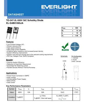
1. Product Overview
This document details the specifications for a high-performance Silicon Carbide (SiC) Schottky Barrier Diode (SBD) housed in a TO-247-2L package. The device is engineered for power electronic applications requiring high efficiency, high-frequency operation, and superior thermal performance. Its core function is to provide unidirectional current flow with minimal switching losses and reverse recovery charge, a significant advantage over traditional silicon PN junction diodes.
The primary positioning of this component is within advanced power conversion systems where efficiency and power density are critical. Its core advantages stem from the fundamental properties of Silicon Carbide, which enable operation at higher temperatures, voltages, and switching frequencies compared to silicon-based devices. The target markets include industrial power supplies, renewable energy systems, and motor drive applications, where these characteristics translate directly into system-level benefits.
2. In-Depth Technical Parameter Analysis
2.1 Absolute Maximum Ratings
The absolute maximum ratings define the stress limits beyond which permanent damage to the device may occur. These are not intended for normal operation.
- Repetitive Peak Reverse Voltage (VRRM): 650V. This is the maximum instantaneous reverse voltage that can be applied repetitively.
- Continuous Forward Current (IF): 10A. This is the maximum DC current the diode can conduct continuously, limited by the maximum junction temperature and thermal resistance.
- Non-Repetitive Surge Current (IFSM): 30A. This rating indicates the diode's ability to withstand a single, high-current overload event (10ms sine half-wave) without failure, which is crucial for handling inrush currents or fault conditions.
- Junction Temperature (TJ): 175\u00b0C. The maximum allowable temperature of the semiconductor junction itself.
- Storage Temperature (TSTG): -55\u00b0C to +175\u00b0C.
2.2 Electrical Characteristics
These parameters define the device's performance under specified test conditions.
- Forward Voltage (VF): Typically 1.48V at IF=10A, TJ=25\u00b0C, with a maximum of 1.85V. This low VF is a key feature of SiC Schottky diodes, leading to reduced conduction losses. Note that VF increases with temperature, reaching approximately 1.9V at TJ=175\u00b0C.
- Reverse Leakage Current (IR): Typically 2\u00b5A at VR=520V, TJ=25\u00b0C, with a maximum of 60\u00b5A. Leakage increases with temperature, a characteristic that must be considered in high-temperature designs.
- Total Capacitive Charge (QC): 15nC (typical) at VR=400V. This is a critical parameter for switching loss calculation. The low QC value signifies that very little energy is stored in the diode's junction capacitance, which must be dissipated during each switching cycle, leading to "essentially no switching losses" as stated in the benefits.
- Capacitance Stored Energy (EC): 2.2\u00b5J (typical) at VR=400V. This is the energy stored in the diode's capacitance at the specified voltage, directly related to QC.
2.3 Thermal Characteristics
Thermal management is paramount for reliable operation and achieving rated performance.
- Thermal Resistance, Junction-to-Case (R\u03b8JC): 1.7\u00b0C/W (typical). This low value indicates excellent heat transfer from the semiconductor die to the device case, allowing heat to be efficiently removed via a heatsink attached to the case. The total power dissipation (PD) rating of 88W at TC=25\u00b0C is derived from this parameter and the maximum junction temperature.
3. Performance Curve Analysis
The datasheet includes several characteristic curves essential for design engineers.
3.1 VF-IF Characteristics
This graph plots forward voltage against forward current, typically at multiple junction temperatures (e.g., 25\u00b0C and 175\u00b0C). It visually demonstrates the low forward voltage drop and its positive temperature coefficient. The positive temperature coefficient is a beneficial trait for parallel operation, as it promotes current sharing and prevents thermal runaway.
3.2 VR-IR Characteristics
This curve shows the relationship between reverse voltage and reverse leakage current, again at different temperatures. It highlights how leakage current remains relatively low until approaching the breakdown region and how it increases exponentially with temperature.
3.3 VR-Ct Characteristics
This graph illustrates how the diode's total capacitance (Ct) decreases with increasing reverse bias voltage (VR). This non-linear capacitance is a key factor in high-frequency switching behavior.
3.4 Maximum Forward Current vs. Case Temperature
This derating curve shows how the maximum allowable continuous forward current (IF) decreases as the case temperature (TC) increases. It is a crucial tool for determining the necessary heatsink performance for a given application current.
3.5 Transient Thermal Impedance
The curve of transient thermal resistance versus pulse width (Z\u03b8JC vs. PW) is vital for evaluating thermal performance under pulsed current conditions. It shows that for very short pulses, the effective thermal resistance is lower than the steady-state R\u03b8JC, allowing higher peak currents.
4. Mechanical and Package Information
4.1 Pin Configuration and Polarity
The device uses a TO-247-2L package with two leads. Pin 1 is the Cathode (K) and Pin 2 is the Anode (A). Importantly, the metal tab or case of the package is electrically connected to the Cathode. This must be carefully considered during mounting to prevent short circuits, as the case must be isolated from the heatsink unless the heatsink is at cathode potential.
4.2 Package Dimensions and Outline
Detailed mechanical drawings are provided with all critical dimensions in millimeters. This includes overall length, width, height, lead spacing, lead diameter, and the dimensions of the mounting hole in the tab. Adherence to these dimensions is necessary for proper PCB footprint design and mechanical assembly.
4.3 Recommended PCB Pad Layout
A suggested footprint for surface-mounting the leads (after forming) is included, specifying pad size, shape, and spacing to ensure reliable soldering and mechanical strength.
5. Assembly and Handling Guidelines
5.1 Mounting Torque
The specified mounting torque for the screw used to attach the device to a heatsink is 8.8 N\u00b7m (or equivalent in lbf-in) for an M3 or 6-32 screw. Applying the correct torque ensures optimal thermal contact without damaging the package.
5.2 Storage Conditions
Devices should be stored within the specified storage temperature range of -55\u00b0C to +175\u00b0C in a dry, non-corrosive environment. Standard ESD (Electrostatic Discharge) precautions should be observed during handling, as the Schottky barrier is sensitive to electrostatic damage.
6. Application Recommendations
6.1 Typical Application Circuits
- Power Factor Correction (PFC): Used as the boost diode in continuous conduction mode (CCM) PFC circuits. Its fast switching and low QC minimize turn-off losses, allowing for higher switching frequencies, which reduces the size of magnetic components.
- Solar Inverters: Employed in the boost stage or within the inverter bridge. The high efficiency reduces power loss, and the high-temperature capability improves reliability in outdoor environments.
- Motor Drives: Used in the freewheeling or clamp diode positions in inverter bridges driving motors. The lack of reverse recovery current reduces voltage spikes and EMI, and improves the efficiency of the drive.
- Uninterruptible Power Supplies (UPS) & Data Center Power Supplies: Similar benefits apply in the high-density, high-efficiency power conversion stages of these systems.
6.2 Critical Design Considerations
- Heatsinking: Due to the high power dissipation capability, proper heatsinking is mandatory for operation at high currents. The thermal resistance from case to ambient (R\u03b8CA) provided by the heatsink must be calculated based on the maximum ambient temperature, power loss, and desired junction temperature margin.
- Paralleling Devices: The positive temperature coefficient of VF facilitates current sharing when multiple diodes are connected in parallel. However, careful layout to ensure symmetric parasitic inductance and resistance is still recommended for optimal sharing.
- Snubber Circuits: While the diode has essentially no reverse recovery, circuit parasitic inductance can still cause voltage overshoot during turn-off. Snubber circuits or careful layout to minimize loop inductance may be necessary in very high di/dt applications.
- Gate Drive Considerations (for associated switches): The fast switching of this diode can lead to high di/dt and dv/dt, which may cause noise coupling into gate drive circuits. Proper shielding and gate drive layout are important.
7. Technical Comparison and Advantages
Compared to standard silicon fast recovery diodes (FRDs) or even silicon carbide junction barrier Schottky (JBS) diodes, this SiC Schottky diode offers distinct advantages:
- Zero Reverse Recovery: The Schottky barrier is a majority carrier device, eliminating the minority carrier storage time and associated reverse recovery current (Qrr) and losses seen in PN junction diodes. This is its most significant advantage.
- Higher Operating Temperature: SiC material allows a maximum junction temperature of 175\u00b0C, higher than typical silicon diodes, enabling operation in harsher environments or with smaller heatsinks.
- Lower Forward Voltage Drop: At typical operating currents, the VF is lower than comparable voltage-rated silicon FRDs, reducing conduction losses.
- Higher Switching Frequency Capability: The combination of low QC and no Qrr enables efficient operation at much higher frequencies, which directly leads to smaller passive components (inductors, capacitors) and increased power density.
8. Frequently Asked Questions (FAQs)
8.1 What does "essentially no switching losses" mean?
It refers to the negligible reverse recovery loss. While there is still capacitive switching loss (related to QC and EC), the complete absence of the much larger reverse recovery loss associated with silicon diodes means the total switching loss is dramatically lower, often an order of magnitude less.
8.2 Why is the case connected to the cathode?
This is a common design in power packages to simplify internal bonding and improve thermal performance. It means the heatsink must be electrically isolated from the rest of the system unless it is intentionally held at the cathode potential. Insulating washers and thermal interface material with high dielectric strength are required.
8.3 How do I calculate the power loss in this diode?
Total power loss (PD) is the sum of conduction loss and switching loss. Conduction loss = IF(AVG) * VF. Switching loss \u2248 (1/2) * C * V^2 * f (for capacitive loss), where C is the effective capacitance, V is the blocking voltage, and f is the switching frequency. The Qrr loss component is zero.
8.4 Can I use this diode to replace a silicon diode directly?
Electrically, in terms of voltage and current rating, often yes. However, the faster switching can expose circuit parasitics, potentially causing higher voltage spikes. The gate drive of the associated switching device (e.g., MOSFET) may need review for noise immunity. Thermal design should also be re-evaluated as the loss profile is different.
9. Design and Usage Case Study
Scenario: Upgrading a 2kW Continuous Conduction Mode (CCM) Power Factor Correction (PFC) boost stage from a silicon ultrafast diode to this SiC Schottky diode. The original design operates at 100kHz.
Analysis: The silicon diode had a Qrr of 50nC and a VF of 1.8V. The switching loss was significant. By replacing it with the SiC diode (QC=15nC, VF=1.48V), the following improvements are realized:
- Switching Loss Reduction: The Qrr loss is eliminated. The capacitive switching loss is reduced due to lower QC.
- Conduction Loss Reduction: Lower VF reduces conduction loss by approximately 18% for the same average current.
- Increased Frequency Potential: The dramatically lower total switching loss allows the designer to increase the switching frequency to 200-300kHz. This reduces the size and weight of the boost inductor and EMI filter components by nearly 50%, directly achieving "increased power density."
- Thermal Management: The overall power loss in the diode is lower. Combined with its higher junction temperature rating, this can allow for a reduction in heatsink size ("reduction of heat sink requirement"), further saving cost and space.
Result: The system efficiency improves by 1-2% at full load, the power density increases, and the system cost may decrease due to smaller magnetics and cooling.
10. Operating Principle Introduction
A Schottky diode is formed by a metal-semiconductor junction, unlike a standard diode's P-N semiconductor junction. In this SiC Schottky diode, a metal contact is made directly to n-type Silicon Carbide. This creates a Schottky barrier which allows current to flow easily in the forward direction when a positive bias is applied to the metal (anode) relative to the semiconductor (cathode).
The key operational difference lies in reverse recovery. In a PN diode, turning it off requires the removal of stored minority carriers (a process called reverse recovery), which takes time and creates a significant reverse current pulse. In a Schottky diode, current is carried only by majority carriers (electrons in n-type SiC). When the voltage reverses, these carriers are swept away almost instantaneously, resulting in no minority carrier storage time and thus "zero reverse recovery." This fundamental principle is what enables the high-speed switching and low switching losses.
11. Technology Trends
Silicon Carbide power devices represent a major trend in power electronics, enabling the transition from traditional silicon-based components. The market drivers are the global push for higher energy efficiency, increased power density, and the electrification of transportation and industry.
The evolution of SiC Schottky diodes focuses on several key areas: further reducing specific on-resistance (which translates to lower VF), improving the reliability and stability of the Schottky metal-semiconductor interface at high temperatures, increasing the voltage rating to 1.2kV, 1.7kV and beyond for medium-voltage applications, and reducing device capacitance (Coss, QC) to enable multi-MHz switching frequencies. Integration is another trend, with the co-packaging of SiC Schottky diodes with SiC MOSFETs into modules to create highly efficient, fast-switching power stages. As manufacturing volumes increase and costs decrease, SiC technology is steadily moving from premium applications into mainstream power conversion products.
LED Specification Terminology
Complete explanation of LED technical terms
Photoelectric Performance
| Term | Unit/Representation | Simple Explanation | Why Important |
|---|---|---|---|
| Luminous Efficacy | lm/W (lumens per watt) | Light output per watt of electricity, higher means more energy efficient. | Directly determines energy efficiency grade and electricity cost. |
| Luminous Flux | lm (lumens) | Total light emitted by source, commonly called "brightness". | Determines if the light is bright enough. |
| Viewing Angle | ° (degrees), e.g., 120° | Angle where light intensity drops to half, determines beam width. | Affects illumination range and uniformity. |
| CCT (Color Temperature) | K (Kelvin), e.g., 2700K/6500K | Warmth/coolness of light, lower values yellowish/warm, higher whitish/cool. | Determines lighting atmosphere and suitable scenarios. |
| CRI / Ra | Unitless, 0–100 | Ability to render object colors accurately, Ra≥80 is good. | Affects color authenticity, used in high-demand places like malls, museums. |
| SDCM | MacAdam ellipse steps, e.g., "5-step" | Color consistency metric, smaller steps mean more consistent color. | Ensures uniform color across same batch of LEDs. |
| Dominant Wavelength | nm (nanometers), e.g., 620nm (red) | Wavelength corresponding to color of colored LEDs. | Determines hue of red, yellow, green monochrome LEDs. |
| Spectral Distribution | Wavelength vs intensity curve | Shows intensity distribution across wavelengths. | Affects color rendering and quality. |
Electrical Parameters
| Term | Symbol | Simple Explanation | Design Considerations |
|---|---|---|---|
| Forward Voltage | Vf | Minimum voltage to turn on LED, like "starting threshold". | Driver voltage must be ≥Vf, voltages add up for series LEDs. |
| Forward Current | If | Current value for normal LED operation. | Usually constant current drive, current determines brightness & lifespan. |
| Max Pulse Current | Ifp | Peak current tolerable for short periods, used for dimming or flashing. | Pulse width & duty cycle must be strictly controlled to avoid damage. |
| Reverse Voltage | Vr | Max reverse voltage LED can withstand, beyond may cause breakdown. | Circuit must prevent reverse connection or voltage spikes. |
| Thermal Resistance | Rth (°C/W) | Resistance to heat transfer from chip to solder, lower is better. | High thermal resistance requires stronger heat dissipation. |
| ESD Immunity | V (HBM), e.g., 1000V | Ability to withstand electrostatic discharge, higher means less vulnerable. | Anti-static measures needed in production, especially for sensitive LEDs. |
Thermal Management & Reliability
| Term | Key Metric | Simple Explanation | Impact |
|---|---|---|---|
| Junction Temperature | Tj (°C) | Actual operating temperature inside LED chip. | Every 10°C reduction may double lifespan; too high causes light decay, color shift. |
| Lumen Depreciation | L70 / L80 (hours) | Time for brightness to drop to 70% or 80% of initial. | Directly defines LED "service life". |
| Lumen Maintenance | % (e.g., 70%) | Percentage of brightness retained after time. | Indicates brightness retention over long-term use. |
| Color Shift | Δu′v′ or MacAdam ellipse | Degree of color change during use. | Affects color consistency in lighting scenes. |
| Thermal Aging | Material degradation | Deterioration due to long-term high temperature. | May cause brightness drop, color change, or open-circuit failure. |
Packaging & Materials
| Term | Common Types | Simple Explanation | Features & Applications |
|---|---|---|---|
| Package Type | EMC, PPA, Ceramic | Housing material protecting chip, providing optical/thermal interface. | EMC: good heat resistance, low cost; Ceramic: better heat dissipation, longer life. |
| Chip Structure | Front, Flip Chip | Chip electrode arrangement. | Flip chip: better heat dissipation, higher efficacy, for high-power. |
| Phosphor Coating | YAG, Silicate, Nitride | Covers blue chip, converts some to yellow/red, mixes to white. | Different phosphors affect efficacy, CCT, and CRI. |
| Lens/Optics | Flat, Microlens, TIR | Optical structure on surface controlling light distribution. | Determines viewing angle and light distribution curve. |
Quality Control & Binning
| Term | Binning Content | Simple Explanation | Purpose |
|---|---|---|---|
| Luminous Flux Bin | Code e.g., 2G, 2H | Grouped by brightness, each group has min/max lumen values. | Ensures uniform brightness in same batch. |
| Voltage Bin | Code e.g., 6W, 6X | Grouped by forward voltage range. | Facilitates driver matching, improves system efficiency. |
| Color Bin | 5-step MacAdam ellipse | Grouped by color coordinates, ensuring tight range. | Guarantees color consistency, avoids uneven color within fixture. |
| CCT Bin | 2700K, 3000K etc. | Grouped by CCT, each has corresponding coordinate range. | Meets different scene CCT requirements. |
Testing & Certification
| Term | Standard/Test | Simple Explanation | Significance |
|---|---|---|---|
| LM-80 | Lumen maintenance test | Long-term lighting at constant temperature, recording brightness decay. | Used to estimate LED life (with TM-21). |
| TM-21 | Life estimation standard | Estimates life under actual conditions based on LM-80 data. | Provides scientific life prediction. |
| IESNA | Illuminating Engineering Society | Covers optical, electrical, thermal test methods. | Industry-recognized test basis. |
| RoHS / REACH | Environmental certification | Ensures no harmful substances (lead, mercury). | Market access requirement internationally. |
| ENERGY STAR / DLC | Energy efficiency certification | Energy efficiency and performance certification for lighting. | Used in government procurement, subsidy programs, enhances competitiveness. |