Table of Contents
- 1. Product Overview
- 1.1 Core Advantages and Target Market
- 2. In-Depth Technical Parameter Analysis
- 2.1 Electrical Characteristics
- 2.2 Thermal Characteristics
- 3. Performance Curve Analysis
- 3.1 VF-IF Characteristics
- 3.2 VR-IR Characteristics
- 3.3 Maximum Forward Current vs. Case Temperature
- 3.4 Transient Thermal Impedance vs. Pulse Width
- 4. Mechanical and Package Information
- 4.1 Package Dimensions and Outline
- 4.2 Pin Configuration and Polarity Identification
- 4.3 Recommended PCB Pad Layout
- 5. Assembly and Handling Guidelines
- 5.1 Mounting Torque
- 5.2 Storage Conditions
- 6. Application Notes and Design Considerations
- 6.1 Typical Application Circuits
- 6.2 Critical Design Considerations
- 7. Technical Comparison and Differentiation
- 8. Frequently Asked Questions (FAQs)
- 9. Operating Principle
- 10. Industry Trends
- LED Specification Terminology
- Photoelectric Performance
- Electrical Parameters
- Thermal Management & Reliability
- Packaging & Materials
- Quality Control & Binning
- Testing & Certification
1. Product Overview
This document details the specifications for a high-performance Silicon Carbide (SiC) Schottky Barrier Diode (SBD) housed in a TO-247-2L package. The device is engineered to leverage the superior material properties of Silicon Carbide, offering significant advantages over traditional silicon-based diodes in high-frequency and high-efficiency power conversion circuits. Its primary function is to serve as a rectifier with minimal switching losses and reverse recovery charge.
1.1 Core Advantages and Target Market
The core advantages of this SiC Schottky diode stem from its fundamental material characteristics. The absence of minority carrier storage eliminates reverse recovery current, a major source of switching loss and electromagnetic interference (EMI) in silicon fast recovery diodes (FRDs) or ultra-fast recovery diodes (UFRDs). This translates to several system-level benefits: enabling higher switching frequencies (which reduces the size of passive components like inductors and capacitors), improving overall system efficiency, and reducing thermal management requirements (smaller heatsinks). The target markets are applications demanding high efficiency, power density, and reliability, including but not limited to Power Factor Correction (PFC) circuits in switched-mode power supplies (SMPS), solar inverters, uninterruptible power supplies (UPS), motor drives, and data center power infrastructure.
2. In-Depth Technical Parameter Analysis
The following sections provide a detailed, objective interpretation of the key electrical and thermal parameters specified in the datasheet. Understanding these parameters is crucial for proper device selection and circuit design.
2.1 Electrical Characteristics
The electrical characteristics define the diode's performance under various operating conditions.
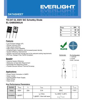
- Repetitive Peak Reverse Voltage (VRRM): 650V - This is the maximum instantaneous reverse voltage that can be applied repetitively. It defines the voltage rating of the device. For reliable operation, the maximum operating voltage in the application should include a safety margin below this value, typically 80-90% of VRRM, depending on the application's voltage spikes and transients.
- Continuous Forward Current (IF): 20A - This is the maximum average forward current the diode can conduct continuously at a specified case temperature (TC=25°C). In real-world applications, the actual permissible current decreases as the junction temperature (TJ) rises. Designers must refer to the derating curves (like the Maximum Ip – TC characteristic) to determine the safe operating current at their specific thermal conditions.
- Forward Voltage (VF): 1.5V (Typ) @ IF=20A, TJ=25°C - This parameter indicates the voltage drop across the diode when conducting. A lower VF reduces conduction losses (Pcond = VF * IF). It's important to note that VF has a negative temperature coefficient for Schottky diodes, meaning it decreases slightly as temperature increases (e.g., typ. 1.9V @ 175°C per the datasheet). This characteristic helps in parallel operation, as a hotter device will naturally draw slightly less current, reducing the risk of thermal runaway.
- Reverse Current (IR): 4µA (Typ) @ VR=520V, TJ=25°C - This is the leakage current when the diode is reverse-biased. While typically very low for SiC, it increases exponentially with temperature (typ. 40µA @ 175°C). This leakage contributes to off-state losses, which are generally negligible compared to switching and conduction losses.
- Total Capacitive Charge (QC): 30nC (Typ) @ VR=400V - This is a critical parameter for high-frequency switching. QC represents the charge associated with the diode's junction capacitance (Cj). During switching, this charge must be supplied or removed, contributing to switching losses. The low QC value of 30nC is a key advantage of SiC Schottky diodes, enabling high-frequency operation with lower associated capacitive switching losses compared to silicon counterparts.
- Surge Non-Repetitive Forward Current (IFSM): 51A - This rating defines the diode's ability to withstand a single, high-current overload event of short duration (10ms sine half-wave). This is important for handling inrush currents or fault conditions in the application.
2.2 Thermal Characteristics
Thermal management is paramount for reliability and performance.
- Junction Temperature (TJ,max): 175°C - The absolute maximum temperature the semiconductor junction can withstand. Continuous operation at or near this limit will severely reduce device lifetime. A common design practice is to limit the maximum operating junction temperature to 125-150°C for improved long-term reliability.
- Thermal Resistance, Junction-to-Case (RθJC): 2.0°C/W (Typ) - This parameter quantifies the thermal impedance between the semiconductor die (junction) and the exterior case of the package. A lower value indicates better heat transfer from the die to the heatsink. The total thermal resistance from junction to ambient (RθJA) is the sum of RθJC, the thermal interface material resistance, and the heatsink resistance. RθJC is used to calculate the junction temperature rise above case temperature: ΔTJ = PD * RθJC, where PD is the power dissipated in the diode.
- Total Power Dissipation (PD): 75W @ TC=25°C - This is the maximum power the device can dissipate when the case is held at 25°C. In practice, this is a theoretical limit used with RθJC to calculate thermal performance. The actual dissipated power must be calculated based on application conditions (conduction and switching losses).
3. Performance Curve Analysis
The datasheet provides several characteristic curves essential for design.
3.1 VF-IF Characteristics
This graph shows the relationship between forward voltage drop and forward current at different junction temperatures. It visually confirms the negative temperature coefficient of VF. Designers use this to accurately calculate conduction losses at their specific operating current and temperature.
3.2 VR-IR Characteristics
This curve plots reverse leakage current against reverse voltage, typically at multiple temperatures. It demonstrates the exponential increase in leakage current with both voltage and temperature, which is crucial for estimating off-state losses in high-temperature environments.
3.3 Maximum Forward Current vs. Case Temperature
This derating curve is one of the most important for design. It shows how the maximum allowable continuous forward current decreases as the case temperature increases. A designer must ensure the application's operating current, after considering all losses and thermal impedance, falls below this curve at the maximum expected case temperature.
3.4 Transient Thermal Impedance vs. Pulse Width
This graph (ZθJC vs. Pulse Width) is critical for evaluating thermal performance during short-duration power pulses, which are common in switching applications. The transient thermal impedance is lower than the steady-state RθJC for short pulses, meaning the junction temperature rise for a given pulse of power is less than what the steady-state RθJC would predict. This allows for higher peak currents in pulsed operation.
4. Mechanical and Package Information
4.1 Package Dimensions and Outline
The device uses the industry-standard TO-247-2L package. Key dimensions from the outline drawing include a total package length of approximately 20.0 mm, a width of 16.26 mm (including leads), and a height of 4.7 mm (excluding leads). The leads have a diameter of 1.0 mm. Precise dimensions are provided in the package outline drawing for PCB footprint design.
4.2 Pin Configuration and Polarity Identification
The TO-247-2L package has two leads and an electrically connected metal tab (case).
Pin 1: Cathode (K).
Pin 2: Anode (A).
Case: This is electrically connected to the Cathode (Pin 1). This connection is vital for thermal and electrical design. The cathode-connected tab must be isolated from the heatsink if the heatsink is at a different potential (e.g., ground). This is typically achieved using an insulating thermal pad and shoulder washers for the mounting screw.
4.3 Recommended PCB Pad Layout
A recommended pad layout for surface mounting (likely referring to a through-hole footprint with thermal relief) is provided. This includes the hole diameters for the leads (e.g., 1.2 mm recommended) and the copper pad dimensions around the holes to ensure good solder fillets and mechanical strength.
5. Assembly and Handling Guidelines
5.1 Mounting Torque
The specified mounting torque for the screw securing the device to a heatsink is 0.8 to 1.0 N·m (or 8.8 lbf·in) for an M3 or 6-32 screw. Applying the correct torque is essential: insufficient torque leads to high thermal resistance, while excessive torque can damage the package or the semiconductor die.
5.2 Storage Conditions
The device can be stored within a temperature range of -55°C to +175°C. It is recommended to store components in a dry, anti-static environment to prevent moisture absorption (which can cause "popcorning" during reflow) and electrostatic discharge (ESD) damage, although Schottky diodes are generally more robust against ESD than MOSFETs.
6. Application Notes and Design Considerations
6.1 Typical Application Circuits
The primary applications highlighted are:
Power Factor Correction (PFC): Used in the boost diode position. Its fast switching and low Qc minimize switching losses at high frequencies (e.g., >100 kHz), improving PFC stage efficiency.
Solar Inverter / UPS: Employed in the input rectification or output inverter freewheeling diode positions. High efficiency reduces energy loss and cooling requirements.
Motor Drives: Used as freewheeling diodes across inverter switches or in brake circuits. The high surge capability (IFSM) is beneficial for handling inductive kickback.
6.2 Critical Design Considerations
- Thermal Design: Calculate total power dissipation (Pcond + Psw) accurately. Use the provided RθJC and derating curves to select an appropriate heatsink and ensure TJ remains within safe limits (e.g., < 150°C). Remember to account for the thermal interface material's resistance.
- Parallel Operation: The negative temperature coefficient of VF facilitates current sharing in parallel configurations, reducing the risk of thermal runaway. However, careful layout symmetry and possibly small gate resistors or current-sharing inductors are still recommended for optimal dynamic current sharing.
- Snubber Circuits: While SiC diodes have essentially no reverse recovery, their junction capacitance and circuit parasitics can still cause voltage overshoot during turn-off. An RC snubber across the diode may be necessary to dampen oscillations and reduce EMI, especially in high-di/dt circuits.
- Gate Drive Consideration (for associated switches): The low Qc of the diode reduces the switching losses of the opposing active switch (e.g., MOSFET, IGBT) in a half-bridge or boost configuration, allowing for potentially simpler or faster gate drives.
7. Technical Comparison and Differentiation
Compared to a silicon PN junction fast recovery diode (FRD) of similar voltage and current rating, this SiC Schottky diode offers decisive advantages:
1. Zero Reverse Recovery (Qrr): The most significant difference. A silicon FRD has a substantial reverse recovery charge (Qrr), causing high switching losses, increased stress on the opposing switch, and significant EMI. The SiC SBD has Qrr ≈ 0.
2. Lower Forward Voltage at High Temperature: While a silicon diode's VF increases with temperature, the SiC SBD's VF decreases, aiding thermal stability.
3. Higher Operating Temperature: SiC material allows a higher maximum junction temperature (175°C vs. typically 150°C for silicon), offering more design headroom.
The trade-off is typically a slightly higher initial cost and a marginally higher forward voltage at room temperature compared to some silicon diodes. However, the system-level savings in efficiency, heatsink size, and magnetics often justify the cost.
8. Frequently Asked Questions (FAQs)
Q: Does this diode require a reverse recovery snubber?
A: Not for the purpose of clamping reverse recovery current, as it is negligible. However, an RC snubber may still be needed to damp high-frequency ringing caused by the diode's junction capacitance resonating with circuit stray inductance.
Q: Can I use this diode directly as a replacement for a silicon FRD in my existing circuit?
A: Electrically, in terms of voltage and current rating, yes. However, you may be able to increase the switching frequency to reduce passive component size. Also, check for any snubber circuits designed for the FRD's Qrr; they might be reduced or eliminated. Thermal performance should be re-evaluated as loss composition changes.
Q: Why is the case connected to the cathode?
A: This is a common configuration. It simplifies isolation in many circuits (like PFC boost stages) where the cathode is often connected to the positive DC bus, which may be isolated from earth ground. If the anode were connected to the case, it would often be at switching node potential, making isolation more complex.
Q: How do I calculate the switching losses for this diode?
A: With Qrr ≈ 0, the primary switching loss component is capacitive. The loss per switching cycle can be approximated as (1/2) * Cj(VR) * VR² * fsw, where Cj is the voltage-dependent junction capacitance, VR is the reverse voltage it switches to, and fsw is the switching frequency. The datasheet provides Cj at specific voltages and the total capacitive energy (EC) curve for more accurate estimation.
9. Operating Principle
A Schottky diode is formed by a metal-semiconductor junction, unlike a standard PN junction diode. In a Silicon Carbide Schottky diode, the semiconductor is SiC. The Schottky barrier formed at the metal-SiC interface allows for majority carrier conduction only (electrons in an N-type SiC). This is the fundamental reason for the absence of minority carrier storage and, consequently, the lack of reverse recovery current. When forward biased, electrons are injected from the semiconductor into the metal. When reverse biased, the Schottky barrier prevents significant current flow, except for a small leakage current. The use of SiC as the semiconductor material provides a wider bandgap than silicon, resulting in higher breakdown electric field strength, higher thermal conductivity, and the ability to operate at higher temperatures.
10. Industry Trends
The adoption of wide-bandgap (WBG) semiconductors like Silicon Carbide (SiC) and Gallium Nitride (GaN) is a dominant trend in power electronics, driven by the global demand for higher energy efficiency and power density. SiC devices, including Schottky diodes and MOSFETs, are seeing rapid cost reduction and performance improvement. Trends include the development of higher voltage ratings (e.g., 1.2kV, 1.7kV) for automotive and industrial applications, lower on-resistance and forward voltage drops, improved reliability data, and the integration of SiC diodes with SiC MOSFETs in power modules. The market is moving towards more optimized and application-specific packages beyond the standard TO-247, such as low-inductance packages like TO-247-4L (with a separate Kelvin source connection for MOSFETs) and various surface-mount packages for compact designs.
LED Specification Terminology
Complete explanation of LED technical terms
Photoelectric Performance
| Term | Unit/Representation | Simple Explanation | Why Important |
|---|---|---|---|
| Luminous Efficacy | lm/W (lumens per watt) | Light output per watt of electricity, higher means more energy efficient. | Directly determines energy efficiency grade and electricity cost. |
| Luminous Flux | lm (lumens) | Total light emitted by source, commonly called "brightness". | Determines if the light is bright enough. |
| Viewing Angle | ° (degrees), e.g., 120° | Angle where light intensity drops to half, determines beam width. | Affects illumination range and uniformity. |
| CCT (Color Temperature) | K (Kelvin), e.g., 2700K/6500K | Warmth/coolness of light, lower values yellowish/warm, higher whitish/cool. | Determines lighting atmosphere and suitable scenarios. |
| CRI / Ra | Unitless, 0–100 | Ability to render object colors accurately, Ra≥80 is good. | Affects color authenticity, used in high-demand places like malls, museums. |
| SDCM | MacAdam ellipse steps, e.g., "5-step" | Color consistency metric, smaller steps mean more consistent color. | Ensures uniform color across same batch of LEDs. |
| Dominant Wavelength | nm (nanometers), e.g., 620nm (red) | Wavelength corresponding to color of colored LEDs. | Determines hue of red, yellow, green monochrome LEDs. |
| Spectral Distribution | Wavelength vs intensity curve | Shows intensity distribution across wavelengths. | Affects color rendering and quality. |
Electrical Parameters
| Term | Symbol | Simple Explanation | Design Considerations |
|---|---|---|---|
| Forward Voltage | Vf | Minimum voltage to turn on LED, like "starting threshold". | Driver voltage must be ≥Vf, voltages add up for series LEDs. |
| Forward Current | If | Current value for normal LED operation. | Usually constant current drive, current determines brightness & lifespan. |
| Max Pulse Current | Ifp | Peak current tolerable for short periods, used for dimming or flashing. | Pulse width & duty cycle must be strictly controlled to avoid damage. |
| Reverse Voltage | Vr | Max reverse voltage LED can withstand, beyond may cause breakdown. | Circuit must prevent reverse connection or voltage spikes. |
| Thermal Resistance | Rth (°C/W) | Resistance to heat transfer from chip to solder, lower is better. | High thermal resistance requires stronger heat dissipation. |
| ESD Immunity | V (HBM), e.g., 1000V | Ability to withstand electrostatic discharge, higher means less vulnerable. | Anti-static measures needed in production, especially for sensitive LEDs. |
Thermal Management & Reliability
| Term | Key Metric | Simple Explanation | Impact |
|---|---|---|---|
| Junction Temperature | Tj (°C) | Actual operating temperature inside LED chip. | Every 10°C reduction may double lifespan; too high causes light decay, color shift. |
| Lumen Depreciation | L70 / L80 (hours) | Time for brightness to drop to 70% or 80% of initial. | Directly defines LED "service life". |
| Lumen Maintenance | % (e.g., 70%) | Percentage of brightness retained after time. | Indicates brightness retention over long-term use. |
| Color Shift | Δu′v′ or MacAdam ellipse | Degree of color change during use. | Affects color consistency in lighting scenes. |
| Thermal Aging | Material degradation | Deterioration due to long-term high temperature. | May cause brightness drop, color change, or open-circuit failure. |
Packaging & Materials
| Term | Common Types | Simple Explanation | Features & Applications |
|---|---|---|---|
| Package Type | EMC, PPA, Ceramic | Housing material protecting chip, providing optical/thermal interface. | EMC: good heat resistance, low cost; Ceramic: better heat dissipation, longer life. |
| Chip Structure | Front, Flip Chip | Chip electrode arrangement. | Flip chip: better heat dissipation, higher efficacy, for high-power. |
| Phosphor Coating | YAG, Silicate, Nitride | Covers blue chip, converts some to yellow/red, mixes to white. | Different phosphors affect efficacy, CCT, and CRI. |
| Lens/Optics | Flat, Microlens, TIR | Optical structure on surface controlling light distribution. | Determines viewing angle and light distribution curve. |
Quality Control & Binning
| Term | Binning Content | Simple Explanation | Purpose |
|---|---|---|---|
| Luminous Flux Bin | Code e.g., 2G, 2H | Grouped by brightness, each group has min/max lumen values. | Ensures uniform brightness in same batch. |
| Voltage Bin | Code e.g., 6W, 6X | Grouped by forward voltage range. | Facilitates driver matching, improves system efficiency. |
| Color Bin | 5-step MacAdam ellipse | Grouped by color coordinates, ensuring tight range. | Guarantees color consistency, avoids uneven color within fixture. |
| CCT Bin | 2700K, 3000K etc. | Grouped by CCT, each has corresponding coordinate range. | Meets different scene CCT requirements. |
Testing & Certification
| Term | Standard/Test | Simple Explanation | Significance |
|---|---|---|---|
| LM-80 | Lumen maintenance test | Long-term lighting at constant temperature, recording brightness decay. | Used to estimate LED life (with TM-21). |
| TM-21 | Life estimation standard | Estimates life under actual conditions based on LM-80 data. | Provides scientific life prediction. |
| IESNA | Illuminating Engineering Society | Covers optical, electrical, thermal test methods. | Industry-recognized test basis. |
| RoHS / REACH | Environmental certification | Ensures no harmful substances (lead, mercury). | Market access requirement internationally. |
| ENERGY STAR / DLC | Energy efficiency certification | Energy efficiency and performance certification for lighting. | Used in government procurement, subsidy programs, enhances competitiveness. |