1. Product Overview
This document provides the complete specification for a high-performance Silicon Carbide (SiC) Schottky Barrier Diode. The device is designed in a surface-mount TO-252-3L (commonly known as DPAK) package, offering a robust solution for high-frequency and high-efficiency power conversion circuits. Unlike conventional silicon PN-junction diodes, this SiC Schottky diode utilizes a metal-semiconductor junction, which fundamentally eliminates reverse recovery charge, a significant source of switching losses and electromagnetic interference (EMI) in power systems.
The core advantage of this component lies in its material properties. Silicon Carbide offers a wider bandgap, higher thermal conductivity, and higher critical electric field strength compared to silicon. These material advantages translate directly into the diode's performance: it can operate at higher voltages, higher temperatures, and with significantly lower switching losses. The target markets for this device are modern power electronics applications where efficiency, power density, and reliability are paramount.
1.1 Key Features and Benefits
The device incorporates several advanced features that provide distinct benefits in system design:
- Low Forward Voltage (VF = 1.5V typical): This reduces conduction losses, directly improving the overall efficiency of the power stage. Lower power dissipation also simplifies thermal management.
- Ultra-Fast Switching with Zero Reverse Recovery Current: The Schottky barrier principle means there is no minority carrier storage. Consequently, the diode switches off almost instantaneously with no reverse recovery current spike. This minimizes switching losses, reduces stress on the controlling switch (e.g., MOSFET), and lowers EMI generation.
- High-Frequency Operation: The absence of reverse recovery allows the diode to be used in circuits operating at hundreds of kHz or even MHz, enabling the use of smaller magnetic components (inductors, transformers) and capacitors, thereby increasing power density.
- High Surge Current Capability (IFSM = 11.8A): The device can withstand short-duration overload currents, such as those encountered during startup or load transients, improving system robustness.
- High Junction Temperature (TJ,max = 175°C): The wide bandgap of SiC allows reliable operation at elevated temperatures, offering a greater safety margin in high-ambient or compact designs.
- Parallel Operation: The positive temperature coefficient of the forward voltage drop helps ensure current sharing between multiple diodes connected in parallel, preventing thermal runaway.
2. In-Depth Technical Parameter Analysis
This section provides a detailed, objective interpretation of the key electrical and thermal parameters specified in the datasheet. Understanding these parameters is critical for reliable circuit design.
2.1 Absolute Maximum Ratings
These ratings define the limits beyond which permanent damage to the device may occur. Operation under or at these limits is not guaranteed.
- Repetitive Peak Reverse Voltage (VRRM): 650V - This is the maximum instantaneous reverse voltage that can be applied repetitively. The circuit's peak voltage, including any ringing or overshoot, must stay below this value.
- Surge Peak Reverse Voltage (VRSM): 650V - This is a non-repetitive rating for surge conditions. It is typically equal to VRRM for Schottky diodes.
- Continuous Forward Current (IF): 6A - This is the maximum DC current the diode can conduct continuously. This rating is limited by the maximum allowable junction temperature and the thermal resistance from junction to case (Rth(JC)). The actual usable current in an application depends heavily on the thermal design (heatsinking, PCB copper area).
- Surge Non-Repetitive Forward Current (IFSM): 11.8A for 10ms half-sine wave - This rating indicates the diode's ability to handle short-term overloads, such as inrush currents. The 10ms pulse width is a common test condition representing a half-cycle of 50Hz AC.
- Junction Temperature (TJ): -55°C to +175°C - The operating and storage temperature range of the semiconductor die itself.
2.2 Electrical Characteristics
These are the typical and maximum/minimum guaranteed performance parameters under specified test conditions.
- Forward Voltage (VF): Typically 1.5V at IF=6A and TJ=25°C, with a maximum of 1.85V. It increases with temperature, reaching about 1.9V at TJ=175°C. This positive temperature coefficient is crucial for parallel operation.
- Reverse Leakage Current (IR): A critical parameter for efficiency, especially at high temperatures. It is typically 0.8µA at VR=520V and TJ=25°C, but can increase to 9µA at TJ=175°C. Designers must account for this leakage in high-temperature, high-voltage applications.
- Total Capacitance (C) and Capacitive Charge (QC): The diode exhibits junction capacitance. The datasheet shows it decreases with increasing reverse voltage (from 173pF at 1V to 15pF at 400V). The Total Capacitive Charge (QC) is a more useful parameter for switching loss calculation, given as 10nC typical at VR=400V. This charge must be dissipated during each switching cycle, contributing to a small capacitive switching loss.
3. Thermal Characteristics
Effective thermal management is essential to realize the device's current rating and long-term reliability.
- Thermal Resistance, Junction-to-Case (Rth(JC)): 4.2°C/W typical. This is the resistance to heat flow from the silicon die to the exposed metal pad (case) of the package. A lower value means heat is more easily transferred out of the die. This parameter is vital for calculating the junction temperature rise above the case temperature: ΔTJ = PD * Rth(JC).
- Power Dissipation (PD): 36W. This is the maximum allowable power dissipation, linked to the Rth(JC) and maximum TJ. In practice, the achievable dissipation is limited by the system's ability to cool the case.
4. Performance Curve Analysis
The typical performance graphs provide visual insight into device behavior under various operating conditions.
4.1 VF-IF Characteristics
This graph shows the relationship between forward voltage drop and forward current at different junction temperatures. Key observations: The curve is relatively linear in the operating range, confirming its Schottky behavior. The voltage drop increases with current and temperature. This graph is used to estimate conduction losses (Pcond = VF * IF).
4.2 VR-IR Characteristics
This graph plots reverse leakage current against reverse voltage, typically at multiple temperatures. It demonstrates the exponential increase of leakage current with both voltage and temperature. This is critical for assessing standby losses and thermal stability in high-voltage blocking states.
4.3 Maximum IF-TC Characteristics
This derating curve shows how the maximum allowable continuous forward current decreases as the case temperature (TC) increases. It is derived from the formula: IF(max) = sqrt((TJ,max - TC) / (Rth(JC) * VF)). Designers must use this graph to select appropriate heatsinking or PCB layout to maintain a low enough case temperature for the required current.
4.4 Transient Thermal Resistance
This graph shows the thermal impedance (Zth) as a function of pulse width. For short current pulses, the effective thermal resistance is lower than the steady-state Rth(JC) because the heat does not have time to spread through the entire system. This graph is essential for evaluating the diode's thermal response to repetitive switching currents or short-duration surge events.
5. Mechanical and Package Information
5.1 Package Outline and Dimensions
The device is housed in a TO-252-3L (DPAK) surface-mount package. Key dimensions from the datasheet include:
- Overall Package Size (D x E): 6.10mm x 6.60mm (typical).
- Package Height (A): 2.30mm (typical).
- Lead Pitch (e): 2.28mm (basic).
- Lead Length (L): 1.52mm (typical).
- Exposed Pad Size (D1 x E1): 5.23mm x 4.83mm (typical).
All tolerances are specified, and designers must refer to the detailed drawing for PCB footprint design.
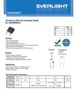
5.2 Pin Configuration and Polarity
The package has three external connections: two leads and the exposed thermal pad.
- Pin 1: Cathode.
- Pin 2: Anode.
- Case (Exposed Pad): Cathode. The exposed pad is electrically connected to the cathode. This is crucial for both electrical circuit connection and thermal management. The pad must be soldered to a cathode-connected copper area on the PCB to act as a heatsink and provide mechanical strength.
5.3 Recommended PCB Pad Layout
The datasheet provides a recommended footprint for surface mounting. This layout is optimized for solder joint reliability and thermal performance. It typically includes a large, centrally located pad for the exposed cathode, with thermal relief connections if needed for soldering, and appropriately sized pads for the anode and cathode leads. Following this recommended layout is essential for proper manufacturing yield and operational reliability.
6. Soldering and Assembly Guidelines
While specific reflow profiles are not provided in this datasheet, standard guidelines for lead-free (Pb-free) SMT assembly apply.
- Reflow Soldering: Use a standard lead-free reflow profile (e.g., IPC/JEDEC J-STD-020). The peak package body temperature should not exceed 260°C. The large thermal mass of the exposed pad may require careful profile tuning to ensure proper solder reflow under the pad without overheating other components.
- Handling: Observe standard ESD (Electrostatic Discharge) precautions, as SiC devices can be sensitive to ESD.
- Storage: Store in a dry, inert environment as per standard moisture sensitivity level (MSL) requirements for SMT packages. The device is likely rated MSL 3 or similar, meaning it must be baked before use if exposed to ambient air beyond its floor life.
7. Application Suggestions
7.1 Typical Application Circuits
This SiC Schottky diode is ideally suited for the following applications:
- Power Factor Correction (PFC) Boost Diode: In continuous conduction mode (CCM) PFC stages, the diode must switch at line frequency (50/60Hz) and high frequency (switching frequency, e.g., 100kHz). The zero reverse recovery characteristic eliminates turn-off losses and associated EMI, making it superior to silicon ultrafast diodes.
- DC-DC Converter Output Rectifier: In boost, buck, or flyback converters, especially those operating at high frequencies to reduce magnetics size.
- Solar Inverter Freewheeling/Blocking Diodes: Used to manage current flow from photovoltaic panels or within the inverter's power stages.
- Motor Drive Circuits: In inverter stages for controlling brushless DC or AC motors.
- High-Efficiency AC/DC and DC/AC Converters: For servers, telecom, and industrial power supplies.
7.2 Design Considerations
- Thermal Design: This is the most critical aspect. The PCB must be designed with a sufficient copper area (on top and bottom layers, connected with vias) under the exposed pad to act as a heatsink. Use the Rth(JC), derating curves, and estimated power losses to calculate the required thermal performance.
- Voltage Rating Selection: Choose a VRRM rating with sufficient margin. For a 400V DC bus, a 650V diode is appropriate, providing margin for voltage spikes and ringing.
- Parallel Operation: Due to the positive temperature coefficient of VF, these diodes can be paralleled to increase current capability. However, careful layout to ensure symmetrical current sharing through matched trace inductance and resistance is still recommended.
- Snubber Circuits: While the diode itself has no reverse recovery, circuit parasitics (stray inductance) can still cause voltage overshoot during turn-off. An RC snubber across the diode may be necessary to dampen these oscillations and protect the diode and the main switch.
8. Technical Comparison and Differentiation
The primary differentiation of this SiC Schottky diode is against two common alternatives:
- vs. Silicon PN Fast/Ultrafast Recovery Diodes: The SiC diode has zero reverse recovery charge (Qrr), while silicon diodes have significant Qrr (tens to hundreds of nC). This eliminates reverse recovery switching losses and associated noise, enabling higher frequency operation and greater efficiency.
- vs. Silicon Schottky Diodes: Silicon Schottky diodes also have low Qrr but are limited to lower voltage ratings (typically below 200V). This SiC device extends the benefits of the Schottky principle to the 650V class, a voltage range dominated by lossy silicon PN diodes.
9. Frequently Asked Questions (Based on Technical Parameters)
Q: The forward voltage is 1.5V, which is higher than a typical silicon Schottky. Isn't this a disadvantage?
A: For low-voltage circuits (<100V), yes, the conduction loss would be higher. However, at 650V, the switching loss savings from zero reverse recovery far outweigh the slightly higher conduction loss. The overall system efficiency is higher with the SiC diode.Q: Can I use this diode for a 400V input PFC circuit?
A: Yes, the 650V rating provides a good safety margin over the nominal 400V DC bus, accounting for line variations and transients.Q: The leakage current at 175°C is 9µA. Is this a concern?
A: For most power conversion applications, this leakage power (Pleak = V*I = 520V * 9µA ≈ 4.7mW) is negligible compared to the total power throughput. However, in very high-impedance or precision circuits, it should be considered.Q: Why is the exposed pad connected to the cathode? How do I heatsink it?
A> The cathode is typically the common or ground node in many circuits (e.g., PFC boost diode). Connecting the pad to the cathode allows it to be attached to a large ground plane on the PCB for excellent thermal dissipation without introducing electrical isolation complexity. You heatsink it by soldering it to a sufficiently large area of cathode-connected copper on the PCB.10. Practical Design Case Study
Scenario: Designing a 500W, 400V output, CCM PFC boost stage operating at 100kHz.
Selection Rationale: A silicon ultrafast diode with comparable rating might have a Qrr of 50nC. The reverse recovery loss per cycle would be Loss_rr = 0.5 * V * Qrr * fsw = 0.5 * 400V * 50nC * 100kHz = 1.0W. This loss generates heat and EMI. The SiC Schottky diode has Qrr ~ 0nC, eliminating this 1W loss entirely. Even with a slightly higher VF, the net system efficiency gain can be 0.5% or more, which is significant at this power level. The thermal design is also simplified due to lower total dissipation.11. Operating Principle
A Schottky diode is formed by a metal-semiconductor junction, unlike a PN junction diode which uses semiconductor-semiconductor. When a positive voltage is applied to the metal (anode) relative to the semiconductor (cathode), electrons flow from the semiconductor into the metal, allowing current (forward bias). Under reverse bias, the built-in potential of the metal-semiconductor barrier blocks current flow. The key distinction is that current is carried only by majority carriers (electrons in an N-type SiC substrate). There are no minority carriers (holes) injected and stored in the drift region. Therefore, when the voltage reverses, there is no stored charge that needs to be removed before the diode can block voltage—hence, zero reverse recovery.
12. Technology Trends
Silicon Carbide power devices represent a major trend in power electronics, driven by demands for higher efficiency, higher power density, and higher temperature operation. The market for SiC diodes and transistors (MOSFETs) is growing rapidly, particularly in electric vehicle onboard chargers, traction inverters, renewable energy systems, and data center power supplies. As manufacturing volumes increase and costs decrease, SiC is moving from a premium technology into broader mainstream applications. Future developments may focus on further reducing specific on-resistance (for MOSFETs), improving gate oxide reliability, and integrating SiC devices with drivers and protection in advanced modules.
LED Specification Terminology
Complete explanation of LED technical terms
Photoelectric Performance
Term Unit/Representation Simple Explanation Why Important Luminous Efficacy lm/W (lumens per watt) Light output per watt of electricity, higher means more energy efficient. Directly determines energy efficiency grade and electricity cost. Luminous Flux lm (lumens) Total light emitted by source, commonly called "brightness". Determines if the light is bright enough. Viewing Angle ° (degrees), e.g., 120° Angle where light intensity drops to half, determines beam width. Affects illumination range and uniformity. CCT (Color Temperature) K (Kelvin), e.g., 2700K/6500K Warmth/coolness of light, lower values yellowish/warm, higher whitish/cool. Determines lighting atmosphere and suitable scenarios. CRI / Ra Unitless, 0–100 Ability to render object colors accurately, Ra≥80 is good. Affects color authenticity, used in high-demand places like malls, museums. SDCM MacAdam ellipse steps, e.g., "5-step" Color consistency metric, smaller steps mean more consistent color. Ensures uniform color across same batch of LEDs. Dominant Wavelength nm (nanometers), e.g., 620nm (red) Wavelength corresponding to color of colored LEDs. Determines hue of red, yellow, green monochrome LEDs. Spectral Distribution Wavelength vs intensity curve Shows intensity distribution across wavelengths. Affects color rendering and quality. Electrical Parameters
Term Symbol Simple Explanation Design Considerations Forward Voltage Vf Minimum voltage to turn on LED, like "starting threshold". Driver voltage must be ≥Vf, voltages add up for series LEDs. Forward Current If Current value for normal LED operation. Usually constant current drive, current determines brightness & lifespan. Max Pulse Current Ifp Peak current tolerable for short periods, used for dimming or flashing. Pulse width & duty cycle must be strictly controlled to avoid damage. Reverse Voltage Vr Max reverse voltage LED can withstand, beyond may cause breakdown. Circuit must prevent reverse connection or voltage spikes. Thermal Resistance Rth (°C/W) Resistance to heat transfer from chip to solder, lower is better. High thermal resistance requires stronger heat dissipation. ESD Immunity V (HBM), e.g., 1000V Ability to withstand electrostatic discharge, higher means less vulnerable. Anti-static measures needed in production, especially for sensitive LEDs. Thermal Management & Reliability
Term Key Metric Simple Explanation Impact Junction Temperature Tj (°C) Actual operating temperature inside LED chip. Every 10°C reduction may double lifespan; too high causes light decay, color shift. Lumen Depreciation L70 / L80 (hours) Time for brightness to drop to 70% or 80% of initial. Directly defines LED "service life". Lumen Maintenance % (e.g., 70%) Percentage of brightness retained after time. Indicates brightness retention over long-term use. Color Shift Δu′v′ or MacAdam ellipse Degree of color change during use. Affects color consistency in lighting scenes. Thermal Aging Material degradation Deterioration due to long-term high temperature. May cause brightness drop, color change, or open-circuit failure. Packaging & Materials
Term Common Types Simple Explanation Features & Applications Package Type EMC, PPA, Ceramic Housing material protecting chip, providing optical/thermal interface. EMC: good heat resistance, low cost; Ceramic: better heat dissipation, longer life. Chip Structure Front, Flip Chip Chip electrode arrangement. Flip chip: better heat dissipation, higher efficacy, for high-power. Phosphor Coating YAG, Silicate, Nitride Covers blue chip, converts some to yellow/red, mixes to white. Different phosphors affect efficacy, CCT, and CRI. Lens/Optics Flat, Microlens, TIR Optical structure on surface controlling light distribution. Determines viewing angle and light distribution curve. Quality Control & Binning
Term Binning Content Simple Explanation Purpose Luminous Flux Bin Code e.g., 2G, 2H Grouped by brightness, each group has min/max lumen values. Ensures uniform brightness in same batch. Voltage Bin Code e.g., 6W, 6X Grouped by forward voltage range. Facilitates driver matching, improves system efficiency. Color Bin 5-step MacAdam ellipse Grouped by color coordinates, ensuring tight range. Guarantees color consistency, avoids uneven color within fixture. CCT Bin 2700K, 3000K etc. Grouped by CCT, each has corresponding coordinate range. Meets different scene CCT requirements. Testing & Certification
Term Standard/Test Simple Explanation Significance LM-80 Lumen maintenance test Long-term lighting at constant temperature, recording brightness decay. Used to estimate LED life (with TM-21). TM-21 Life estimation standard Estimates life under actual conditions based on LM-80 data. Provides scientific life prediction. IESNA Illuminating Engineering Society Covers optical, electrical, thermal test methods. Industry-recognized test basis. RoHS / REACH Environmental certification Ensures no harmful substances (lead, mercury). Market access requirement internationally. ENERGY STAR / DLC Energy efficiency certification Energy efficiency and performance certification for lighting. Used in government procurement, subsidy programs, enhances competitiveness.