Table of Contents
- 1. Product Overview
- 2. In-Depth Technical Parameter Analysis
- 2.1 Electrical Characteristics
- 2.2 Thermal Characteristics
- 3. Performance Curve Analysis
- 3.1 Forward Characteristics (VF-IF)
- 3.2 Reverse Characteristics and Capacitance
- 3.3 Surge and Transient Performance
- 4. Mechanical and Package Information
- 4.1 Package Outline and Dimensions
- 4.2 Pin Configuration and Polarity Identification
- 5. Soldering and Assembly Guidelines
- 6. Application Recommendations
- 6.1 Typical Application Circuits
- 6.2 Design Considerations
- 7. Technical Comparison and Advantages
- 8. Frequently Asked Questions (FAQ)
- 9. Practical Design Case Study
- 10. Operating Principle
- 11. Technology Trends
1. Product Overview
This document details the specifications for a high-performance Silicon Carbide (SiC) Schottky Barrier Diode (SBD) in a surface-mount TO-252-3L (DPAK) package. The device is engineered for high-voltage, high-frequency power conversion applications where efficiency, power density, and thermal management are critical. Utilizing SiC technology, this diode offers superior switching characteristics compared to traditional silicon PN junction diodes, enabling significant system-level improvements.
The core advantage of this SiC Schottky diode lies in its near-zero reverse recovery charge, which virtually eliminates switching losses associated with diode turn-off. This characteristic is paramount for increasing switching frequencies in power supplies and inverters, allowing for the use of smaller passive components like inductors and capacitors, thereby increasing overall power density. The low forward voltage drop further contributes to reduced conduction losses, enhancing system efficiency across the operating temperature range.
2. In-Depth Technical Parameter Analysis
2.1 Electrical Characteristics
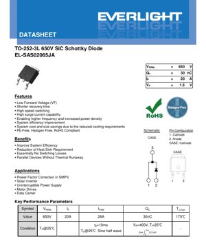
The device is rated for a maximum repetitive peak reverse voltage (VRRM) of 650V, making it suitable for applications operating from universal AC mains (85-265VAC) with sufficient design margin. The continuous forward current (IF) rating is 20A, determined at a case temperature (TC) of 25°C. It is crucial to note that this current rating is thermally limited and will derate with increasing junction temperature, as detailed in the thermal characteristics section.
A key performance parameter for switching diodes is the total capacitive charge (Qc). This device specifies a typical Qc of 30nC at a reverse voltage (VR) of 400V and a junction temperature (Tj) of 25°C. This low value confirms the minimal stored charge, which directly translates to low switching losses and enables high-frequency operation. The forward voltage (VF) is specified at a maximum of 1.85V when conducting 16A at 25°C, rising to a typical 1.9V at the maximum junction temperature of 175°C. This positive temperature coefficient of VF is a beneficial trait of SiC Schottky diodes, promoting current sharing and preventing thermal runaway when multiple devices are operated in parallel.
The reverse leakage current (IR) is exceptionally low, with a maximum of 120µA at 520V and 25°C. This low leakage contributes to high efficiency, especially in standby or light-load conditions.
2.2 Thermal Characteristics
Effective thermal management is essential for reliable operation. The primary thermal metric is the junction-to-case thermal resistance (RθJC), which is specified at a typical value of 3.6°C/W. This low value indicates efficient heat transfer from the semiconductor junction to the package case, allowing heat to be effectively dissipated via an external heatsink attached to the tab. The maximum allowable junction temperature (Tj) is 175°C, and the device can be stored within a temperature range of -55°C to +175°C.
The total power dissipation (PD) is rated at 50W at TC=25°C. In practical applications, the actual permissible power dissipation is calculated based on the maximum junction temperature, the thermal resistance (junction-to-ambient, RθJA, which includes case-to-heatsink and heatsink-to-ambient resistances), and the ambient temperature. The provided "Power Dissipation" and "Transient Thermal Resistance" curves are critical for designing for transient overload conditions and determining safe operating areas.
3. Performance Curve Analysis
3.1 Forward Characteristics (VF-IF)
The VF-IF characteristic curve illustrates the relationship between forward voltage drop and forward current at various junction temperatures. As expected for a Schottky diode, the curve shows a lower knee voltage compared to silicon PN diodes. The curve also demonstrates the positive temperature coefficient, where VF increases with Tj for a given current. This graph is essential for calculating conduction losses (Ploss = VF * IF) under different operating conditions.
3.2 Reverse Characteristics and Capacitance
The VR-IR curve shows the very low reverse leakage current over the voltage range up to the blocking voltage. The VR-Ct curve displays the junction capacitance as a function of reverse bias. Capacitance decreases with increasing reverse voltage (from ~513pF at 1V to ~46pF at 400V), which is a characteristic of the voltage-dependent depletion region width. The low and voltage-dependent capacitance impacts the switching speed and the Qc parameter.
3.3 Surge and Transient Performance
The "Maximum Ip – TC Characteristics" chart defines the permissible non-repetitive surge current (IFSM) as a function of case temperature. The device can handle a 26A surge (half-sine wave, 10ms duration) at 25°C. The "IFSM – PW Characteristics" graph further details the surge current capability versus pulse width, which is vital for designing protection against inrush currents or fault conditions. The "EC-VR Characteristics" curve plots the stored capacitive energy (EC) against reverse voltage, important for understanding losses in resonant circuits.
4. Mechanical and Package Information
4.1 Package Outline and Dimensions
The device is housed in a TO-252-3L package. Critical dimensions include an overall package length (E) of 6.60mm (typ), width (D) of 6.10mm (typ), and height (A) of 2.30mm (typ). The lead pitch (e1) is 2.28mm (basic). The large metal tab (case) serves as the primary thermal path and is electrically connected to the cathode terminal. A detailed dimensioned drawing with tolerances is provided for PCB footprint design.
4.2 Pin Configuration and Polarity Identification
The pin configuration is clearly defined: Pin 1 is the Cathode (K), Pin 2 is the Anode (A), and the CASE (the large metal tab) is also connected to the Cathode. Correct polarity identification during assembly is crucial to prevent device failure. The recommended PCB pad layout for surface mounting is provided to ensure proper solder joint formation and thermal connection to the board.
5. Soldering and Assembly Guidelines
As a surface-mount component, this diode is intended for reflow soldering processes. While specific reflow profile parameters (preheat, soak, reflow peak temperature, time above liquidus) are not listed in this datasheet, standard lead-free (Pb-Free) reflow profiles compliant with IPC/JEDEC J-STD-020 should be followed. The maximum package body temperature during soldering should not exceed the specified storage temperature maximum of 175°C for an extended period. The mounting torque for any screw used with the tab (if applicable for heatsinking) is specified as 8.8 N·cm (1 lbf·in) for M3 or 6-32 screws.
Precautions should be taken to avoid mechanical stress on the leads after soldering. The device should be stored in a dry, anti-static environment prior to use to prevent moisture absorption (which can cause "popcorning" during reflow) and electrostatic discharge damage.
6. Application Recommendations
6.1 Typical Application Circuits
This SiC Schottky diode is ideally suited for several high-performance power conversion topologies:
- Power Factor Correction (PFC) in Switch-Mode Power Supplies (SMPS): Used as the boost diode in continuous conduction mode (CCM) or critical conduction mode (CrM) PFC stages. Its fast switching and low Qc reduce switching losses at high line frequencies, improving efficiency, especially at high line voltages.
- Solar Inverters: Employed in the boost stage of photovoltaic micro-inverters or string inverters to handle high voltages and currents with minimal loss, maximizing energy harvest.
- Uninterruptible Power Supplies (UPS): Used in the inverter output stage or battery charging circuits for efficient high-frequency switching.
- Motor Drives: Can be used in freewheeling or clamp circuits within variable frequency drives (VFDs) to manage inductive kickback from motors efficiently.
- Data Center Power Supplies: Essential for achieving high efficiency (e.g., 80 Plus Titanium) in server power supplies where every percentage point of loss reduction is critical.
6.2 Design Considerations
Thermal Design: The primary design challenge is managing junction temperature. Utilize the RθJC value and the maximum Tj to calculate the required heatsinking. The metal tab must be soldered to a sufficiently large copper pad on the PCB, potentially with thermal vias to inner layers or a backside plane, to act as a heatsink. For higher power applications, an external heatsink attached to the tab may be necessary.
Parallel Operation: The positive temperature coefficient of VF facilitates current sharing among paralleled diodes. However, careful layout symmetry is still required to ensure equal parasitic inductance and resistance in each branch, preventing current imbalance during fast transients.
Snubber Circuits: While the diode has very low recovery charge, parasitic circuit inductance and capacitance can still cause voltage overshoot during turn-off. Snubber circuits (RC or RCD) may be needed to clamp these spikes and ensure reliable operation within the maximum voltage ratings.
Gate Drive Considerations (for associated switches): The fast switching of this diode can lead to high di/dt and dv/dt. This may necessitate attention to the gate drive design of the accompanying switching transistor (e.g., MOSFET) to avoid false triggering due to Miller effect or to manage electromagnetic interference (EMI).
7. Technical Comparison and Advantages
Compared to standard silicon fast recovery diodes (FRDs) or even silicon carbide junction barrier Schottky (JBS) diodes, this Schottky diode offers distinct advantages:
- Zero Reverse Recovery: The Schottky barrier mechanism has no minority carrier storage, leading to the near-zero Qc. This eliminates reverse recovery current spikes, reducing switching losses in the diode itself and the accompanying transistor, and minimizing EMI.
- High-Temperature Operation: SiC material properties allow a maximum junction temperature of 175°C, higher than typical silicon devices (150°C), offering greater design margin or allowing for smaller heatsinks.
- High Frequency Capability: The combination of low Qc and low capacitance enables efficient operation at switching frequencies well into the hundreds of kHz, surpassing the practical limits of silicon FRDs.
- Efficiency Gains: The lower VF (compared to Si PN diodes at high temperature) and absence of recovery losses directly translate to higher system efficiency, particularly at partial load and high line conditions.
8. Frequently Asked Questions (FAQ)
Q: Can this diode replace a silicon fast recovery diode directly in an existing design?
A: While electrically it may be a pin-compatible replacement, a design review is mandatory. The faster switching can exacerbate voltage spikes due to circuit parasitics. Thermal performance will also differ. Snubber values and heatsinking should be re-evaluated.
Q: Why is the case connected to the cathode? Does this require isolation?
A: Yes, the metal tab is electrically live (at cathode potential). The PCB pad it connects to must be on the cathode net. If the tab is attached to an external heatsink, that heatsink must be electrically isolated from other potentials or the system chassis, unless the chassis is also at cathode potential.
Q: How is the surge current rating (IFSM) applied?
A: The IFSM rating of 26A (10ms, half-sine) is for non-repetitive events like startup inrush or fault clearance. It should not be used for calculating continuous current capability. The "IFSM – PW" curve must be consulted for other pulse durations.
Q: What is the significance of the Capacitance Stored Energy (EC) parameter?
A: In applications like LLC resonant converters, the diode's output capacitance (Coss) is discharged each switching cycle, causing loss. EC quantifies this loss. Lower EC means lower capacitive switching loss.
9. Practical Design Case Study
Scenario: Designing a 1kW, 80 Plus Titanium efficiency PFC stage for a server power supply.
The design uses a interleaved critical conduction mode (CrM) topology switching at 100kHz. Each phase handles 500W. The boost diode must block up to 400VDC and carry a peak current of approximately 10A. A silicon ultrafast diode was initially considered but calculated to have over 5W of recovery-related loss per phase at high line.
By substituting this 650V SiC Schottky diode, the recovery loss is eliminated. The remaining losses are primarily conduction loss (based on VF and RMS current) and a small capacitive loss (based on EC). The thermal calculation, using RθJC=3.6°C/W and a designed Tj max of 125°C, shows the diode junction temperature rise is manageable with the PCB copper area as the primary heatsink. This substitution directly contributes to meeting the >96% efficiency requirement at 230VAC input for the Titanium standard, while also allowing the magnetics to be smaller due to the high, clean switching frequency.
10. Operating Principle
A Schottky diode is formed by a metal-semiconductor junction, as opposed to the p-n semiconductor junction of a standard diode. In this SiC Schottky diode, a metal contact is made to n-type Silicon Carbide. This creates a Schottky barrier which allows current to flow easily in the forward direction when a positive bias is applied to the metal (anode) relative to the semiconductor (cathode). In reverse bias, the barrier widens, blocking current flow.
The critical distinction is that current transport is dominated by majority carriers (electrons in n-type SiC). There is no injection, storage, and subsequent removal of minority carriers (holes) as in a PN junction diode. Therefore, when the diode is switched from forward conduction to reverse blocking, there is no reverse recovery current spike or associated delay time. The diode turns off almost instantaneously, limited only by the charging of its junction capacitance. This fundamental principle is the source of its high-speed switching performance and low switching losses.
11. Technology Trends
Silicon Carbide power devices represent a significant trend in power electronics, enabling higher efficiency, power density, and operating temperatures than silicon-based devices. For diodes, the evolution is towards higher voltage ratings (now commonly 650V and 1200V, with 1700V and 3300V emerging), lower forward voltage drops, and reduced capacitance. The TO-252-3L (DPAK) package used here is a workhorse for surface-mount power, but there is a parallel trend towards even lower-inductance, better-thermally-performing packages like TOLL (TO-leadless) and D2PAK-7L for the highest performance applications. Integration is another trend, with co-packaged SiC MOSFET and Schottky diode "half-bridge" modules becoming available to minimize parasitic inductance in switching cells. The continued reduction in the cost of SiC substrates is making this technology accessible for a broader range of applications beyond premium server and telecom power supplies, including automotive onboard chargers, industrial motor drives, and consumer appliances seeking higher efficiency standards.
LED Specification Terminology
Complete explanation of LED technical terms
Photoelectric Performance
| Term | Unit/Representation | Simple Explanation | Why Important |
|---|---|---|---|
| Luminous Efficacy | lm/W (lumens per watt) | Light output per watt of electricity, higher means more energy efficient. | Directly determines energy efficiency grade and electricity cost. |
| Luminous Flux | lm (lumens) | Total light emitted by source, commonly called "brightness". | Determines if the light is bright enough. |
| Viewing Angle | ° (degrees), e.g., 120° | Angle where light intensity drops to half, determines beam width. | Affects illumination range and uniformity. |
| CCT (Color Temperature) | K (Kelvin), e.g., 2700K/6500K | Warmth/coolness of light, lower values yellowish/warm, higher whitish/cool. | Determines lighting atmosphere and suitable scenarios. |
| CRI / Ra | Unitless, 0–100 | Ability to render object colors accurately, Ra≥80 is good. | Affects color authenticity, used in high-demand places like malls, museums. |
| SDCM | MacAdam ellipse steps, e.g., "5-step" | Color consistency metric, smaller steps mean more consistent color. | Ensures uniform color across same batch of LEDs. |
| Dominant Wavelength | nm (nanometers), e.g., 620nm (red) | Wavelength corresponding to color of colored LEDs. | Determines hue of red, yellow, green monochrome LEDs. |
| Spectral Distribution | Wavelength vs intensity curve | Shows intensity distribution across wavelengths. | Affects color rendering and quality. |
Electrical Parameters
| Term | Symbol | Simple Explanation | Design Considerations |
|---|---|---|---|
| Forward Voltage | Vf | Minimum voltage to turn on LED, like "starting threshold". | Driver voltage must be ≥Vf, voltages add up for series LEDs. |
| Forward Current | If | Current value for normal LED operation. | Usually constant current drive, current determines brightness & lifespan. |
| Max Pulse Current | Ifp | Peak current tolerable for short periods, used for dimming or flashing. | Pulse width & duty cycle must be strictly controlled to avoid damage. |
| Reverse Voltage | Vr | Max reverse voltage LED can withstand, beyond may cause breakdown. | Circuit must prevent reverse connection or voltage spikes. |
| Thermal Resistance | Rth (°C/W) | Resistance to heat transfer from chip to solder, lower is better. | High thermal resistance requires stronger heat dissipation. |
| ESD Immunity | V (HBM), e.g., 1000V | Ability to withstand electrostatic discharge, higher means less vulnerable. | Anti-static measures needed in production, especially for sensitive LEDs. |
Thermal Management & Reliability
| Term | Key Metric | Simple Explanation | Impact |
|---|---|---|---|
| Junction Temperature | Tj (°C) | Actual operating temperature inside LED chip. | Every 10°C reduction may double lifespan; too high causes light decay, color shift. |
| Lumen Depreciation | L70 / L80 (hours) | Time for brightness to drop to 70% or 80% of initial. | Directly defines LED "service life". |
| Lumen Maintenance | % (e.g., 70%) | Percentage of brightness retained after time. | Indicates brightness retention over long-term use. |
| Color Shift | Δu′v′ or MacAdam ellipse | Degree of color change during use. | Affects color consistency in lighting scenes. |
| Thermal Aging | Material degradation | Deterioration due to long-term high temperature. | May cause brightness drop, color change, or open-circuit failure. |
Packaging & Materials
| Term | Common Types | Simple Explanation | Features & Applications |
|---|---|---|---|
| Package Type | EMC, PPA, Ceramic | Housing material protecting chip, providing optical/thermal interface. | EMC: good heat resistance, low cost; Ceramic: better heat dissipation, longer life. |
| Chip Structure | Front, Flip Chip | Chip electrode arrangement. | Flip chip: better heat dissipation, higher efficacy, for high-power. |
| Phosphor Coating | YAG, Silicate, Nitride | Covers blue chip, converts some to yellow/red, mixes to white. | Different phosphors affect efficacy, CCT, and CRI. |
| Lens/Optics | Flat, Microlens, TIR | Optical structure on surface controlling light distribution. | Determines viewing angle and light distribution curve. |
Quality Control & Binning
| Term | Binning Content | Simple Explanation | Purpose |
|---|---|---|---|
| Luminous Flux Bin | Code e.g., 2G, 2H | Grouped by brightness, each group has min/max lumen values. | Ensures uniform brightness in same batch. |
| Voltage Bin | Code e.g., 6W, 6X | Grouped by forward voltage range. | Facilitates driver matching, improves system efficiency. |
| Color Bin | 5-step MacAdam ellipse | Grouped by color coordinates, ensuring tight range. | Guarantees color consistency, avoids uneven color within fixture. |
| CCT Bin | 2700K, 3000K etc. | Grouped by CCT, each has corresponding coordinate range. | Meets different scene CCT requirements. |
Testing & Certification
| Term | Standard/Test | Simple Explanation | Significance |
|---|---|---|---|
| LM-80 | Lumen maintenance test | Long-term lighting at constant temperature, recording brightness decay. | Used to estimate LED life (with TM-21). |
| TM-21 | Life estimation standard | Estimates life under actual conditions based on LM-80 data. | Provides scientific life prediction. |
| IESNA | Illuminating Engineering Society | Covers optical, electrical, thermal test methods. | Industry-recognized test basis. |
| RoHS / REACH | Environmental certification | Ensures no harmful substances (lead, mercury). | Market access requirement internationally. |
| ENERGY STAR / DLC | Energy efficiency certification | Energy efficiency and performance certification for lighting. | Used in government procurement, subsidy programs, enhances competitiveness. |