Table of Contents
- 1. Product Overview
- 2. In-Depth Technical Parameter Analysis
- 2.1 Electrical Characteristics
- 2.2 Maximum Ratings and Thermal Characteristics
- 3. Performance Curve Analysis
- 3.1 Forward Characteristics (VF-IF)
- 3.2 Reverse Characteristics (VR-IR)
- 3.3 Capacitance Characteristics (VR-Ct)
- 3.4 Surge Current Derating (IFSM – PW)
- 3.5 Transient Thermal Impedance (ZθJC)
- 4. Mechanical and Package Information
- 4.1 Package Outline and Dimensions
- 4.2 Pin Configuration and Polarity
- 4.3 Recommended PCB Pad Layout
- 5. Soldering and Assembly Guidelines
- 6. Application Suggestions
- 6.1 Typical Application Circuits
- 6.2 Design Considerations
- 7. Technical Comparison and Advantages
- 8. Frequently Asked Questions (FAQs)
- 9. Practical Design Case Study
- 10. Operating Principle
- 11. Technology Trends
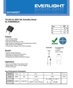
1. Product Overview
This document details the specifications for a high-performance Silicon Carbide (SiC) Schottky Barrier Diode (SBD) housed in a TO-252-3L (DPAK) surface-mount package. The device is engineered for high-voltage, high-frequency power conversion applications where efficiency, thermal performance, and switching speed are critical. The core technology leverages the superior material properties of Silicon Carbide, which enables operation at higher temperatures, voltages, and switching frequencies compared to traditional silicon-based diodes.
The primary positioning of this component is as a rectifier or freewheeling diode in advanced power supply topologies. Its inherent characteristics make it an ideal choice for modern, high-density power designs aiming to minimize losses and reduce the size of passive components and heat sinks.
2. In-Depth Technical Parameter Analysis
2.1 Electrical Characteristics
The electrical parameters define the operational boundaries and performance under specific conditions.
- Repetitive Peak Reverse Voltage (VRRM): 650V. This is the maximum instantaneous reverse voltage the diode can withstand repeatedly. It defines the voltage class of the device and is crucial for selecting diodes in circuits like Power Factor Correction (PFC) or inverter bridges operating from rectified mains voltage.
- Continuous Forward Current (IF): 8A at a case temperature (TC) of 135°C. This rating indicates the diode's current-carrying capability under continuous conduction, limited by its thermal dissipation. The specification at a high case temperature highlights its robust thermal performance.
- Forward Voltage (VF): Typically 1.5V at 8A and 25°C junction temperature (TJ), with a maximum of 1.85V. This parameter directly impacts conduction losses. The relatively low VF for a SiC device contributes to higher system efficiency. Note that VF has a negative temperature coefficient, meaning it decreases as the junction temperature rises, which is a characteristic of Schottky diodes.
- Reverse Current (IR): Maximum 40 µA at 520V and 25°C. This leakage current is exceptionally low, even at high reverse voltages and elevated temperatures (max 20 µA at 175°C), minimizing off-state losses.
- Total Capacitive Charge (QC): 12 nC typical at 400V. This is a key figure of merit for switching performance. A lower QC means less charge needs to be displaced during each switching cycle, leading to lower switching losses and enabling higher frequency operation.
2.2 Maximum Ratings and Thermal Characteristics
These parameters define the absolute limits for safe operation and the device's ability to manage heat.
- Surge Non-Repetitive Forward Current (IFSM): 14.4A for a 10ms half-sine wave. This rating is vital for surviving short-circuit events, inrush currents, or other transient overload conditions.
- Junction Temperature (TJ): Maximum 175°C. The high maximum operating temperature is a direct benefit of the SiC material, allowing for operation in harsh environments or enabling more compact designs with higher power density.
- Thermal Resistance, Junction-to-Case (RθJC): 3.7 °C/W typical. This low thermal resistance indicates efficient heat transfer from the semiconductor junction to the package case. It is a critical parameter for thermal management design, as it determines how much the junction temperature will rise for a given power dissipation. A lower RθJC allows for higher power handling or the use of a smaller heat sink.
- Total Power Dissipation (PD): 40W. This is the maximum power the device can dissipate, governed by the thermal resistance and maximum junction temperature.
3. Performance Curve Analysis
The datasheet includes several characteristic curves essential for detailed design and simulation.
3.1 Forward Characteristics (VF-IF)
This graph plots forward voltage drop against forward current at various junction temperatures. Designers use this to accurately calculate conduction losses under different operating conditions. The curve will show the typical exponential relationship, with the voltage drop being lower at higher temperatures for a given current.
3.2 Reverse Characteristics (VR-IR)
This curve illustrates the reverse leakage current as a function of the applied reverse voltage. It confirms the low leakage current specified in the table across the operating voltage range.
3.3 Capacitance Characteristics (VR-Ct)
This plot shows the junction capacitance (Ct) versus reverse voltage (VR). Capacitance decreases non-linearly as reverse voltage increases. This information is critical for predicting switching behavior, as the stored charge (QC) is the integral of this capacitance over voltage. The decreasing capacitance with voltage is a favorable trait for high-voltage switching.
3.4 Surge Current Derating (IFSM – PW)
This characteristic shows how the allowable surge current (IFSM) decreases as the pulse width (PW) increases. It provides guidance for designing protection circuits or assessing fault condition survivability beyond the standard 10ms rating.
3.5 Transient Thermal Impedance (ZθJC)
This curve is crucial for evaluating thermal performance under pulsed power conditions. It shows the effective thermal resistance from junction to case for single pulses of varying duration. For short pulses, the thermal impedance is much lower than the steady-state RθJC, meaning the junction can handle higher instantaneous power without overheating. This is key for applications with high peak currents.
4. Mechanical and Package Information
4.1 Package Outline and Dimensions
The device uses the industry-standard TO-252-3L (DPAK) surface-mount package. Key dimensions from the datasheet include:
- Package body length (D): 6.10 mm (typ)
- Package body width (E): 6.60 mm (typ)
- Overall height (H): 9.84 mm (typ)
- Lead pitch (e1): 2.28 mm (basic)
- Lead length (L): 1.52 mm (typ)
Detailed mechanical drawings with minimum, typical, and maximum values for all critical dimensions are provided to ensure proper PCB footprint design and assembly clearance.
4.2 Pin Configuration and Polarity
The TO-252-3L package has three connection points: two leads and the exposed metal tab (case).
- Pin 1: Cathode (K)
- Pin 2: Anode (A)
- Case (Tab): Connected to the Cathode (K)
Important Note: The case is electrically connected to the cathode. This must be considered during PCB layout to prevent accidental short circuits. The tab provides the primary path for heat dissipation and must be soldered to an appropriately sized copper pad on the PCB.
4.3 Recommended PCB Pad Layout
A suggested footprint for the surface-mount pads is included. This layout is optimized for solder joint reliability and thermal performance. It typically features a large central pad for the thermal tab (cathode) to maximize heat transfer into the PCB copper, with two smaller pads for the anode and cathode leads. Following this recommendation helps achieve proper solder fillets and minimizes thermal stress.
5. Soldering and Assembly Guidelines
While specific reflow profiles are not detailed in this excerpt, general guidelines for surface-mount devices in TO-252 packages apply.
- Reflow Soldering: Standard lead-free (Pb-free) reflow profiles with a peak temperature not exceeding 260°C are typically suitable. The large thermal mass of the tab may require careful profile tuning to ensure all solder joints reach proper reflow temperature.
- Handling: Standard ESD (Electrostatic Discharge) precautions should be observed, as with all semiconductor devices.
- Storage: Devices should be stored in a dry, controlled environment. The specified storage temperature range is -55°C to +175°C.
6. Application Suggestions
6.1 Typical Application Circuits
- Boost Diode in PFC Stages: Its fast switching and low QC minimize switching losses at high frequencies (e.g., 65-100 kHz), improving PFC efficiency. The high VRRM is suitable for universal input (85-265VAC) designs.
- Output Rectifier in LLC Resonant Converters: The zero reverse recovery characteristic eliminates reverse recovery losses, which is a major advantage in high-frequency resonant topologies, leading to cooler operation and higher efficiency.
- Freewheeling/Clamping Diode in Motor Drives and Inverters: Used in parallel with switching MOSFETs or IGBTs to provide a path for inductive load current. Fast switching prevents voltage spikes and reduces stress on the main switch.
- Solar Micro-inverters and String Inverters: Benefits from high efficiency and high-temperature operation in outdoor environments.
- High-Density AC/DC and DC/DC Converters: The combination of high frequency capability and high-temperature rating allows for smaller magnetics and heat sinks, increasing power density.
6.2 Design Considerations
- Thermal Management: Despite its low RθJC, proper heatsinking is essential. The PCB pad for the tab must be connected to large copper planes or an external heatsink to utilize the full current and power ratings. Thermal vias under the pad can help transfer heat to inner or bottom layers.
- Paralleling Devices: The datasheet mentions the benefit of "Parallel Devices Without Thermal Runaway." This is due to the positive temperature coefficient of the forward voltage in SiC Schottky diodes. As one device gets hotter, its VF increases slightly, causing current to be shared more evenly with cooler parallel devices, promoting stable current sharing.
- Snubber Circuits: While the diode itself is very fast, circuit parasitics (stray inductance) can still cause voltage overshoot during turn-off. Snubber circuits (RC or RCD) may be necessary in some high-di/dt applications to clamp these spikes and protect the diode and other components.
- Gate Drive Considerations (for associated switches): The fast switching of this diode can lead to high di/dt and dv/dt. This may require attention to the gate drive design of the companion MOSFET/IGBT to avoid issues like false triggering due to Miller effect.
7. Technical Comparison and Advantages
Compared to standard silicon fast recovery diodes (FRDs) or even silicon carbide MOSFET body diodes, this SiC Schottky diode offers distinct advantages:
- Zero Reverse Recovery Current (Qrr=0): This is its most significant advantage over silicon PN junction diodes. It completely eliminates reverse recovery losses and associated switching noise, enabling higher efficiency and frequency.
- Lower Forward Voltage than Early SiC Diodes: Modern SiC Schottky diodes have significantly reduced VF, closing the gap with silicon diodes while retaining all high-speed and high-temperature benefits.
- Higher Operating Temperature: 175°C max junction temperature vs. typically 150°C for silicon, offering greater design margin and reliability in hot environments.
- Superior Surge Capability: Good IFSM rating for its size, providing robustness.
- Vs. SiC MOSFET Body Diode: While a SiC MOSFET's body diode is also a PIN diode with poor reverse recovery, using a separate SiC Schottky as the freewheeling diode is often preferred in hard-switching circuits to avoid the body diode's losses.
8. Frequently Asked Questions (FAQs)
Q: What does "Zero Reverse Recovery" practically mean for my design?
A: It means you can ignore reverse recovery losses in your efficiency calculations. It also simplifies snubber design and reduces electromagnetic interference (EMI) generated during diode turn-off.
Q: The case is connected to the cathode. How do I isolate it if needed?
A: Electrical isolation requires using an insulating thermal pad (e.g., mica, silicone) between the diode tab and the heatsink, along with an insulating shoulder washer for the mounting screw. This adds thermal resistance, so the trade-off must be calculated.
Q: Can I use this diode at its full 8A rating continuously?
A: Only if you can maintain the case temperature at or below 135°C. The actual continuous current will be lower if the thermal design results in a higher case temperature. Use the power dissipation (PD) and thermal resistance (RθJC) to calculate the maximum allowable power loss for your specific heatsink and ambient conditions, then derive the current from the VF curve.
Q: Why is the QC parameter important?
A: QC represents the energy stored in the diode's junction capacitance. During turn-on of the opposing switch in a circuit, this charge must be removed, causing a current spike. Lower QC reduces this spike, lowering switching losses in the control switch and reducing stress on both components.
9. Practical Design Case Study
Scenario: Designing a 500W, 80Plus Titanium efficiency server power supply unit (PSU) with a bridgeless totem-pole PFC stage operating at 100 kHz.
Challenge: Traditional silicon ultrafast diodes in the PFC boost position exhibit significant reverse recovery losses at 100 kHz, limiting efficiency and causing thermal management issues.
Solution: Implementing the 650V SiC Schottky diode as the boost diode.
Implementation & Outcome:
1. The diode is placed in the standard boost diode position.
2. Due to its zero reverse recovery, the turn-off switching loss is virtually eliminated.
3. The low Qc reduces the turn-on loss of the complementary MOSFET.
4. The high 175°C rating allows it to be placed close to other hot components.
5. Result: Measured PFC stage efficiency increases by ~0.7% at full load compared to the best silicon alternative. This directly contributes to meeting the stringent Titanium efficiency standard. Furthermore, the diode runs cooler, allowing for a more compact layout or reduced airflow requirement, increasing power density.
10. Operating Principle
A Schottky diode is formed by a metal-semiconductor junction, unlike a standard PN junction diode which uses a semiconductor-semiconductor junction. In a Silicon Carbide Schottky diode, the semiconductor is SiC. The metal-SiC junction creates a Schottky barrier which allows for majority carrier conduction only (electrons in an N-type SiC). This is in contrast to a PN diode, where conduction involves both majority and minority carriers (diffusion current).
The absence of minority carrier injection and storage is the fundamental reason for the lack of reverse recovery. When the voltage across a Schottky diode reverses, there is no stored minority charge that needs to be swept out of the drift region; the current simply ceases almost instantaneously once the carriers are depleted from the junction. This results in the "zero reverse recovery" characteristic. The fast switching is a direct consequence of this unipolar conduction mechanism.
11. Technology Trends
Silicon Carbide power devices are a key enabling technology for the ongoing trend towards higher efficiency, higher frequency, and higher power density across all segments of power electronics. The market for SiC diodes is driven by several factors:
- Electric Vehicles (EVs): Demand for faster on-board chargers (OBCs), more efficient DC-DC converters, and traction inverters with higher switching frequencies.
- Renewable Energy: Solar and wind inverters benefit from the higher efficiency, which increases energy yield, and the higher temperature capability, which improves reliability in outdoor installations.
- Data Centers & Telecom: The push for higher efficiency (e.g., 80Plus Titanium) and increased rack power density necessitates the use of advanced components like SiC diodes in server PSUs and rectifiers.
- Industrial Motor Drives: Seeking higher control bandwidth and efficiency.
The trend for SiC Schottky diodes specifically is towards lower forward voltage drop (reducing conduction loss), higher current density (smaller die size for a given rating), and improved reliability and cost reduction through manufacturing scale and process maturity. Integration with SiC MOSFETs in multi-chip modules is also a growing trend.
LED Specification Terminology
Complete explanation of LED technical terms
Photoelectric Performance
| Term | Unit/Representation | Simple Explanation | Why Important |
|---|---|---|---|
| Luminous Efficacy | lm/W (lumens per watt) | Light output per watt of electricity, higher means more energy efficient. | Directly determines energy efficiency grade and electricity cost. |
| Luminous Flux | lm (lumens) | Total light emitted by source, commonly called "brightness". | Determines if the light is bright enough. |
| Viewing Angle | ° (degrees), e.g., 120° | Angle where light intensity drops to half, determines beam width. | Affects illumination range and uniformity. |
| CCT (Color Temperature) | K (Kelvin), e.g., 2700K/6500K | Warmth/coolness of light, lower values yellowish/warm, higher whitish/cool. | Determines lighting atmosphere and suitable scenarios. |
| CRI / Ra | Unitless, 0–100 | Ability to render object colors accurately, Ra≥80 is good. | Affects color authenticity, used in high-demand places like malls, museums. |
| SDCM | MacAdam ellipse steps, e.g., "5-step" | Color consistency metric, smaller steps mean more consistent color. | Ensures uniform color across same batch of LEDs. |
| Dominant Wavelength | nm (nanometers), e.g., 620nm (red) | Wavelength corresponding to color of colored LEDs. | Determines hue of red, yellow, green monochrome LEDs. |
| Spectral Distribution | Wavelength vs intensity curve | Shows intensity distribution across wavelengths. | Affects color rendering and quality. |
Electrical Parameters
| Term | Symbol | Simple Explanation | Design Considerations |
|---|---|---|---|
| Forward Voltage | Vf | Minimum voltage to turn on LED, like "starting threshold". | Driver voltage must be ≥Vf, voltages add up for series LEDs. |
| Forward Current | If | Current value for normal LED operation. | Usually constant current drive, current determines brightness & lifespan. |
| Max Pulse Current | Ifp | Peak current tolerable for short periods, used for dimming or flashing. | Pulse width & duty cycle must be strictly controlled to avoid damage. |
| Reverse Voltage | Vr | Max reverse voltage LED can withstand, beyond may cause breakdown. | Circuit must prevent reverse connection or voltage spikes. |
| Thermal Resistance | Rth (°C/W) | Resistance to heat transfer from chip to solder, lower is better. | High thermal resistance requires stronger heat dissipation. |
| ESD Immunity | V (HBM), e.g., 1000V | Ability to withstand electrostatic discharge, higher means less vulnerable. | Anti-static measures needed in production, especially for sensitive LEDs. |
Thermal Management & Reliability
| Term | Key Metric | Simple Explanation | Impact |
|---|---|---|---|
| Junction Temperature | Tj (°C) | Actual operating temperature inside LED chip. | Every 10°C reduction may double lifespan; too high causes light decay, color shift. |
| Lumen Depreciation | L70 / L80 (hours) | Time for brightness to drop to 70% or 80% of initial. | Directly defines LED "service life". |
| Lumen Maintenance | % (e.g., 70%) | Percentage of brightness retained after time. | Indicates brightness retention over long-term use. |
| Color Shift | Δu′v′ or MacAdam ellipse | Degree of color change during use. | Affects color consistency in lighting scenes. |
| Thermal Aging | Material degradation | Deterioration due to long-term high temperature. | May cause brightness drop, color change, or open-circuit failure. |
Packaging & Materials
| Term | Common Types | Simple Explanation | Features & Applications |
|---|---|---|---|
| Package Type | EMC, PPA, Ceramic | Housing material protecting chip, providing optical/thermal interface. | EMC: good heat resistance, low cost; Ceramic: better heat dissipation, longer life. |
| Chip Structure | Front, Flip Chip | Chip electrode arrangement. | Flip chip: better heat dissipation, higher efficacy, for high-power. |
| Phosphor Coating | YAG, Silicate, Nitride | Covers blue chip, converts some to yellow/red, mixes to white. | Different phosphors affect efficacy, CCT, and CRI. |
| Lens/Optics | Flat, Microlens, TIR | Optical structure on surface controlling light distribution. | Determines viewing angle and light distribution curve. |
Quality Control & Binning
| Term | Binning Content | Simple Explanation | Purpose |
|---|---|---|---|
| Luminous Flux Bin | Code e.g., 2G, 2H | Grouped by brightness, each group has min/max lumen values. | Ensures uniform brightness in same batch. |
| Voltage Bin | Code e.g., 6W, 6X | Grouped by forward voltage range. | Facilitates driver matching, improves system efficiency. |
| Color Bin | 5-step MacAdam ellipse | Grouped by color coordinates, ensuring tight range. | Guarantees color consistency, avoids uneven color within fixture. |
| CCT Bin | 2700K, 3000K etc. | Grouped by CCT, each has corresponding coordinate range. | Meets different scene CCT requirements. |
Testing & Certification
| Term | Standard/Test | Simple Explanation | Significance |
|---|---|---|---|
| LM-80 | Lumen maintenance test | Long-term lighting at constant temperature, recording brightness decay. | Used to estimate LED life (with TM-21). |
| TM-21 | Life estimation standard | Estimates life under actual conditions based on LM-80 data. | Provides scientific life prediction. |
| IESNA | Illuminating Engineering Society | Covers optical, electrical, thermal test methods. | Industry-recognized test basis. |
| RoHS / REACH | Environmental certification | Ensures no harmful substances (lead, mercury). | Market access requirement internationally. |
| ENERGY STAR / DLC | Energy efficiency certification | Energy efficiency and performance certification for lighting. | Used in government procurement, subsidy programs, enhances competitiveness. |