1. Product Overview
The EL827 series represents a family of phototransistor-based photocouplers (optocouplers) housed in an industry-standard 8-pin Dual In-line Package (DIP). These devices are designed to provide electrical isolation and signal transmission between circuits operating at different voltage potentials or impedances. The core function is achieved through an infrared emitting diode (IRED) optically coupled to a silicon phototransistor detector. This configuration allows control signals to pass from the input side to the output side while maintaining a high degree of electrical isolation, which is critical for safety and noise immunity in many electronic systems.
The primary advantage of this series lies in its combination of a high current transfer ratio (CTR) range and a robust isolation voltage rating. The compact DIP package is available in several lead form options, including standard, wide-lead spacing, and surface-mount types, providing flexibility for different PCB assembly processes. The devices are compliant with major international safety and environmental standards, making them suitable for a wide range of global applications.
1.1 Core Features and Target Applications
The EL827 series is engineered with several key features that define its performance envelope and application suitability. A high Current Transfer Ratio (CTR) ranging from 50% to 600% (at IF=5mA, VCE=5V) ensures efficient signal transfer with good sensitivity. The isolation voltage between the input and output sections is rated at 5000 Vrms, providing a strong barrier against high-voltage transients and enhancing system safety.
The product is compliant with RoHS and EU REACH regulations. It has received safety approvals from several renowned international agencies including UL, cUL (file E214129), VDE (file 132249), SEMKO, NEMKO, DEMKO, FIMKO, and CQC. These certifications are essential for products destined for markets with strict safety requirements.
Typical applications for the EL827 series include:
- Programmable Logic Controllers (PLCs) and industrial automation systems.
- System appliances and precision measuring instruments requiring noise-free signal acquisition.
- Telecommunication equipment for signal isolation and interface protection.
- Home appliances, such as fan heaters and other control systems.
- General-purpose signal transmission between circuits of different potentials and impedances, serving as a fundamental isolation component.
2. Technical Specifications and In-Depth Interpretation
This section provides a detailed breakdown of the device's electrical and optical parameters. Understanding these specifications is crucial for proper circuit design and ensuring reliable long-term operation.
2.1 Absolute Maximum Ratings
The Absolute Maximum Ratings define the stress limits beyond which permanent damage to the device may occur. Operation under or at these limits is not guaranteed and should be avoided in normal use. The ratings are specified at an ambient temperature (Ta) of 25°C.
- Input (Diode) Side: The continuous forward current (IF) must not exceed 60 mA. A brief peak forward current (IFP) of 1 A for 1 microsecond is permissible. The maximum reverse voltage (VR) applied to the diode is 6 V. The power dissipation on the input side (PD) is limited to 100 mW.
- Output (Transistor) Side: The maximum collector current (IC) is 50 mA. The collector-emitter voltage (VCEO) can be up to 80 V, while the emitter-collector voltage (VECO) is limited to 7 V. The output power dissipation (PC) is 150 mW.
- Device Totals and Environmental: The total device power dissipation (PTOT) is 200 mW. The isolation voltage (VISO) between the input and output sections is 5000 Vrms (tested for 1 minute at 40-60% relative humidity). The operating temperature range (TOPR) is from -55°C to +110°C, and the storage temperature (TSTG) ranges from -55°C to +125°C. The soldering temperature (TSOL) should not exceed 260°C for 10 seconds during assembly.
2.2 Electro-Optical Characteristics
These parameters define the device's performance under normal operating conditions, typically at Ta=25°C. They are essential for calculating circuit performance.
Input Characteristics (Infrared Emitting Diode):
- Forward Voltage (VF): Typically 1.2V, with a maximum of 1.4V when a forward current (IF) of 20 mA is applied. This parameter is used to size the current-limiting resistor for the input side.
- Reverse Current (IR): Maximum of 10 µA when a reverse voltage (VR) of 4V is applied, indicating the diode's leakage in the off state.
- Input Capacitance (Cin): Typically 30 pF, with a maximum of 250 pF (measured at 0V, 1 kHz). This affects high-frequency switching performance.
Output Characteristics (Phototransistor):
- Collector-Emitter Dark Current (ICEO): Maximum of 100 nA when VCE=20V and IF=0mA. This is the leakage current of the phototransistor when no light is incident.
- Breakdown Voltages: The collector-emitter breakdown voltage (BVCEO) is a minimum of 80V (IC=0.1mA). The emitter-collector breakdown voltage (BVECO) is a minimum of 7V (IE=0.1mA).
Transfer Characteristics (Coupling Performance):
- Current Transfer Ratio (CTR): This is the key parameter, defined as (IC / IF) * 100%. For the EL827 series, it ranges from a minimum of 50% to a maximum of 600% under the standard test condition of IF=5mA and VCE=5V. This wide range may indicate different grades or production spreads. Designers must account for the minimum CTR to ensure the output transistor saturates properly.
- Collector-Emitter Saturation Voltage (VCE(sat)): Typically 0.1V, with a maximum of 0.2V when IF=20mA and IC=1mA. A low VCE(sat) is desirable for output switching applications to minimize voltage drop.
- Isolation Resistance (RIO): Minimum of 5 x 10^10 Ω when 500V DC is applied between the isolated sides. This indicates excellent DC isolation.
- Floating Capacitance (CIO): Typically 0.6 pF, maximum 1.0 pF (VIO=0V, f=1MHz). This small capacitance contributes to high common-mode transient immunity.
- Cut-off Frequency (fc): Typically 80 kHz (VCE=5V, IC=2mA, RL=100Ω, -3dB point). This defines the small-signal bandwidth of the device.
- Switching Times: Rise time (tr) is typically 3 µs (max 18 µs), and fall time (tf) is typically 4 µs (max 18 µs) under the specified test conditions (VCE=2V, IC=2mA, RL=100Ω). These times determine the maximum digital switching speed.
3. Performance Curve Analysis
The datasheet references typical electro-optical characteristic curves. While the specific graphs are not reproduced in the provided text, their purpose is to illustrate how key parameters vary with operating conditions. Designers should consult the full datasheet for these graphs.
Typical Curves would include:
- CTR vs. Forward Current (IF): Shows how the current transfer ratio changes with the input diode current. CTR often peaks at a specific IF and may decrease at very high currents due to heating or other effects.
- CTR vs. Ambient Temperature (Ta): Illustrates the temperature dependence of the coupling efficiency. CTR typically decreases as temperature increases.
- Output Current (IC) vs. Collector-Emitter Voltage (VCE): Family of curves with IF as a parameter, similar to a standard transistor's output characteristics. This shows the operating regions (saturation, active).
- Saturation Voltage (VCE(sat)) vs. Forward Current (IF): Shows the relationship between input drive and output transistor saturation.
3.1 Switching Time Test Circuit
Figure 10 in the datasheet details the standard test circuit and waveform definitions for measuring switching times (ton, toff, tr, tf). The test is conducted with a pulsed input current driving the IRED. The output is monitored across a load resistor (RL) connected between the collector and a supply voltage (VCC). The rise time (tr) is measured from 10% to 90% of the output pulse's final value, and the fall time (tf) is measured from 90% to 10%. Understanding this test setup helps designers replicate conditions if they need to characterize the device in their specific application circuit.
4. Mechanical and Package Information
The EL827 is offered in an 8-pin DIP package with several lead form options to accommodate different PCB designs and assembly methods.
4.1 Pin Configuration and Schematic
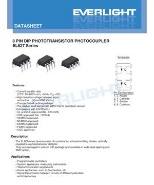
The internal schematic shows an infrared emitting diode connected between pins 1/3 (anode) and 2/4 (cathode). The phototransistor's emitter is connected to pins 5/7, and its collector is connected to pins 6/8. Pins with the same function are internally connected to provide mechanical strength and potentially lower lead inductance. The standard connection is to use one pin from each pair.
Pin Assignment:
- Pin 1, 3: Anode (A)
- Pin 2, 4: Cathode (K)
- Pin 5, 7: Emitter (E)
- Pin 6, 8: Collector (C)
4.2 Package Dimensions and Options
Detailed mechanical drawings are provided for each package variant:
- Standard DIP Type: The conventional through-hole package.
- Option M Type: Features a \"wide lead bend\" providing a 0.4-inch (approx. 10.16mm) lead spacing, which may be useful for breadboarding or specific layout requirements.
- Option S Type: Surface-mount lead form for reflow soldering.
- Option S1 Type: A \"low profile\" surface-mount lead form, likely with a reduced stand-off height compared to the S option.
The datasheet also includes a recommended pad layout for the surface-mount options (S and S1), which is critical for achieving reliable solder joints and proper mechanical alignment during reflow soldering.
4.3 Device Marking
Devices are marked on the top with \"EL827\" denoting the series, followed by a one-digit year code (Y), a two-digit week code (WW), and an optional \"V\" suffix if the unit is VDE-approved. This marking allows for traceability of manufacturing date and variant.
5. Soldering and Assembly Guidelines
5.1 Soldering Conditions
The datasheet provides critical information for the assembly process, particularly for surface-mount variants. The maximum allowable body temperature during soldering is defined by a reflow profile referenced to IPC/JEDEC J-STD-020D. Key parameters of this profile include:
- Preheat Temperature: Minimum (Tsmin) 150°C, Maximum (Tsmax) 200°C.
- Time in Preheat: The profile shows a specific time (ts) in this temperature range to gradually heat the component and board, minimizing thermal shock.
- Peak Temperature & Time: The profile must not exceed the maximum soldering temperature (TSOL) of 260°C, and the time above 260°C should be limited (typically to 10 seconds as noted in the Absolute Maximum Ratings).
Adhering to this profile is essential to prevent damage to the plastic package, the internal wire bonds, or the semiconductor die itself. For through-hole parts, wave soldering or hand soldering should also respect the 260°C for 10 seconds limit.
6. Packaging and Ordering Information
6.1 Ordering Part Number Structure
The part number follows the format: EL827X(Z)-V
- X: Lead form option: None (Standard DIP), M (Wide lead bend), S (Surface mount), S1 (Low profile surface mount).
- Z: Tape and reel option: None (tube packed), TA, or TB (different tape feed directions).
- V: Optional VDE safety approval marking.
6.2 Packing Quantities
- Standard DIP and Option M: 45 units per tube.
- Options S(TA), S(TB), S1(TA), S1(TB): 1000 units per reel.
6.3 Tape and Reel Specifications
Detailed dimensions for the carrier tape are provided for the S and S1 options (TA and TB). Parameters include pocket dimensions (A, B, Do, D1), tape pitch (Po, P1), tape thickness (t), and overall tape width (W). Options TA and TB differ in the direction of feed from the reel, which must be correctly configured in the pick-and-place machine. Diagrams show the orientation of the device within the tape pocket.
7. Application Suggestions and Design Considerations
When designing with the EL827 photocoupler, several factors must be considered to ensure optimal performance and reliability.
Input Circuit Design: A current-limiting resistor must be placed in series with the input IRED. Its value is calculated based on the supply voltage (Vcc_in), the desired forward current (IF), and the diode's forward voltage (VF): R_in = (Vcc_in - VF) / IF. The chosen IF affects CTR, switching speed, and device longevity. Operating at or below the recommended 20mA for continuous operation is advisable.
Output Circuit Design: The phototransistor can be used in either a switching (saturation) mode or a linear (active) mode. For digital switching, a pull-up resistor (RL) is connected between the collector and the output-side supply voltage (Vcc_out). The value of RL influences switching speed (lower RL = faster, but higher IC) and current consumption. Ensure the output current (IC) does not exceed the 50mA maximum. For linear applications, the device operates in its active region, but the nonlinear CTR and temperature dependence must be carefully accounted for.
Isolation and Layout: To maintain the high isolation rating, maintain adequate creepage and clearance distances on the PCB between the input and output side copper traces, as per relevant safety standards (e.g., IEC 60950-1, IEC 62368-1). Place the photocoupler straddling the isolation barrier in the layout.
Bypassing and Noise: For noise-sensitive applications or to improve stability in switching circuits, consider placing a small bypass capacitor (e.g., 0.1 µF) close to the supply pins on both the input and output sides of the device.
8. Technical Comparison and Common Questions
8.1 Differentiation from Other Photocouplers
The EL827's primary differentiators are its high 5000Vrms isolation voltage and wide CTR range (50-600%). Compared to basic 4-pin photocouplers, the 8-pin DIP offers dual pins for each terminal, which can improve mechanical board retention and potentially offer slightly better thermal performance. The availability of surface-mount (S, S1) and wide-lead (M) options provides more flexibility than many single-package offerings. The comprehensive set of international safety approvals (UL, VDE, etc.) is a significant advantage for commercial and industrial products requiring certification.
8.2 Frequently Asked Questions (Based on Parameters)
Q: What does a CTR range of 50-600% mean for my design?
A: It indicates production variation. You must design your circuit to work reliably with the minimum guaranteed CTR (50% in this case) to ensure the output switches properly under all conditions. If your design requires a specific sensitivity, you may need to select devices based on measured CTR (binning) or use a circuit that compensates for the variation.
Q: Can I use this for analog signal isolation?
A: While possible (using it in linear mode), it is not ideal due to the nonlinearity of CTR with respect to IF and its strong temperature dependence. For precision analog isolation, dedicated linear optocouplers or isolation amplifiers are recommended.
Q: How do I choose between the S and S1 surface-mount options?
A: The S1 \"low profile\" option is designed for applications with strict height restrictions on the PCB assembly. Consult the package dimension drawings in the datasheet to compare the standoff height and overall dimensions. The electrical characteristics are identical.
Q: The switching times seem slow (up to 18µs). Is this suitable for my high-speed digital communication?
A> For standard digital I/O isolation in PLCs or microcontroller interfaces, these speeds are typically sufficient. For high-speed serial communication (e.g., USB, RS-485 isolation), much faster digital isolators (based on capacitive or magnetic coupling) or high-speed optocouplers specifically designed for data rates in the Mbps range should be considered.
9. Operational Principles and Trends
9.1 Basic Operating Principle
A photocoupler operates by converting an electrical signal into light, transmitting that light across an electrically insulating gap, and then converting the light back into an electrical signal. In the EL827, an electrical current applied to the input Infrared Emitting Diode (IRED) causes it to emit photons (light) at an infrared wavelength. This light travels through a transparent insulating mold compound and strikes the base region of the silicon phototransistor on the output side. The incident light generates electron-hole pairs in the base, effectively acting as a base current, which allows a much larger collector current to flow. This collector current is proportional to the intensity of the incident light, which in turn is proportional to the input diode current, establishing the current transfer ratio (CTR). The key point is that the only connection between the input and output is the beam of light, providing the electrical isolation.
9.2 Industry Trends
The market for optocouplers continues to evolve. Key trends include a push for higher data rates to accommodate faster industrial communication protocols and digital power supply control. There is also a demand for higher integration, such as combining multiple isolation channels in a single package or integrating additional functions like gate drivers for IGBTs/MOSFETs. Furthermore, the need for enhanced reliability, particularly in automotive and industrial applications, drives improvements in high-temperature performance and long-term stability of the CTR. While traditional phototransistor-based couplers like the EL827 remain workhorses for basic isolation due to their simplicity, cost-effectiveness, and high voltage capability, newer technologies like capacitive and magnetic (giant magnetoresistance) isolators are gaining share in applications requiring very high speed, low power consumption, and robust noise immunity.
LED Specification Terminology
Complete explanation of LED technical terms
Photoelectric Performance
| Term | Unit/Representation | Simple Explanation | Why Important |
|---|---|---|---|
| Luminous Efficacy | lm/W (lumens per watt) | Light output per watt of electricity, higher means more energy efficient. | Directly determines energy efficiency grade and electricity cost. |
| Luminous Flux | lm (lumens) | Total light emitted by source, commonly called "brightness". | Determines if the light is bright enough. |
| Viewing Angle | ° (degrees), e.g., 120° | Angle where light intensity drops to half, determines beam width. | Affects illumination range and uniformity. |
| CCT (Color Temperature) | K (Kelvin), e.g., 2700K/6500K | Warmth/coolness of light, lower values yellowish/warm, higher whitish/cool. | Determines lighting atmosphere and suitable scenarios. |
| CRI / Ra | Unitless, 0–100 | Ability to render object colors accurately, Ra≥80 is good. | Affects color authenticity, used in high-demand places like malls, museums. |
| SDCM | MacAdam ellipse steps, e.g., "5-step" | Color consistency metric, smaller steps mean more consistent color. | Ensures uniform color across same batch of LEDs. |
| Dominant Wavelength | nm (nanometers), e.g., 620nm (red) | Wavelength corresponding to color of colored LEDs. | Determines hue of red, yellow, green monochrome LEDs. |
| Spectral Distribution | Wavelength vs intensity curve | Shows intensity distribution across wavelengths. | Affects color rendering and quality. |
Electrical Parameters
| Term | Symbol | Simple Explanation | Design Considerations |
|---|---|---|---|
| Forward Voltage | Vf | Minimum voltage to turn on LED, like "starting threshold". | Driver voltage must be ≥Vf, voltages add up for series LEDs. |
| Forward Current | If | Current value for normal LED operation. | Usually constant current drive, current determines brightness & lifespan. |
| Max Pulse Current | Ifp | Peak current tolerable for short periods, used for dimming or flashing. | Pulse width & duty cycle must be strictly controlled to avoid damage. |
| Reverse Voltage | Vr | Max reverse voltage LED can withstand, beyond may cause breakdown. | Circuit must prevent reverse connection or voltage spikes. |
| Thermal Resistance | Rth (°C/W) | Resistance to heat transfer from chip to solder, lower is better. | High thermal resistance requires stronger heat dissipation. |
| ESD Immunity | V (HBM), e.g., 1000V | Ability to withstand electrostatic discharge, higher means less vulnerable. | Anti-static measures needed in production, especially for sensitive LEDs. |
Thermal Management & Reliability
| Term | Key Metric | Simple Explanation | Impact |
|---|---|---|---|
| Junction Temperature | Tj (°C) | Actual operating temperature inside LED chip. | Every 10°C reduction may double lifespan; too high causes light decay, color shift. |
| Lumen Depreciation | L70 / L80 (hours) | Time for brightness to drop to 70% or 80% of initial. | Directly defines LED "service life". |
| Lumen Maintenance | % (e.g., 70%) | Percentage of brightness retained after time. | Indicates brightness retention over long-term use. |
| Color Shift | Δu′v′ or MacAdam ellipse | Degree of color change during use. | Affects color consistency in lighting scenes. |
| Thermal Aging | Material degradation | Deterioration due to long-term high temperature. | May cause brightness drop, color change, or open-circuit failure. |
Packaging & Materials
| Term | Common Types | Simple Explanation | Features & Applications |
|---|---|---|---|
| Package Type | EMC, PPA, Ceramic | Housing material protecting chip, providing optical/thermal interface. | EMC: good heat resistance, low cost; Ceramic: better heat dissipation, longer life. |
| Chip Structure | Front, Flip Chip | Chip electrode arrangement. | Flip chip: better heat dissipation, higher efficacy, for high-power. |
| Phosphor Coating | YAG, Silicate, Nitride | Covers blue chip, converts some to yellow/red, mixes to white. | Different phosphors affect efficacy, CCT, and CRI. |
| Lens/Optics | Flat, Microlens, TIR | Optical structure on surface controlling light distribution. | Determines viewing angle and light distribution curve. |
Quality Control & Binning
| Term | Binning Content | Simple Explanation | Purpose |
|---|---|---|---|
| Luminous Flux Bin | Code e.g., 2G, 2H | Grouped by brightness, each group has min/max lumen values. | Ensures uniform brightness in same batch. |
| Voltage Bin | Code e.g., 6W, 6X | Grouped by forward voltage range. | Facilitates driver matching, improves system efficiency. |
| Color Bin | 5-step MacAdam ellipse | Grouped by color coordinates, ensuring tight range. | Guarantees color consistency, avoids uneven color within fixture. |
| CCT Bin | 2700K, 3000K etc. | Grouped by CCT, each has corresponding coordinate range. | Meets different scene CCT requirements. |
Testing & Certification
| Term | Standard/Test | Simple Explanation | Significance |
|---|---|---|---|
| LM-80 | Lumen maintenance test | Long-term lighting at constant temperature, recording brightness decay. | Used to estimate LED life (with TM-21). |
| TM-21 | Life estimation standard | Estimates life under actual conditions based on LM-80 data. | Provides scientific life prediction. |
| IESNA | Illuminating Engineering Society | Covers optical, electrical, thermal test methods. | Industry-recognized test basis. |
| RoHS / REACH | Environmental certification | Ensures no harmful substances (lead, mercury). | Market access requirement internationally. |
| ENERGY STAR / DLC | Energy efficiency certification | Energy efficiency and performance certification for lighting. | Used in government procurement, subsidy programs, enhances competitiveness. |