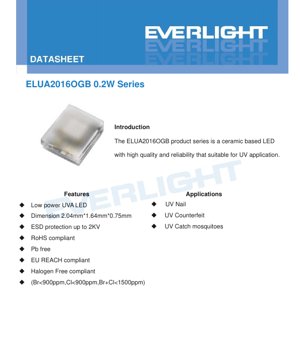
1. Product Overview
The ELUA2016OGB product series represents a high-reliability, ceramic-based LED solution specifically engineered for ultraviolet (UVA) applications. This series is designed to deliver consistent performance in demanding environments, leveraging a robust Al2O3 ceramic package for superior thermal management and longevity. The primary positioning of this product is within the low-to-mid power UVA segment, targeting applications where a compact form factor, reliability, and specific spectral output are critical. Its core advantages include a very small footprint of 2.04mm x 1.64mm, making it suitable for space-constrained designs, integrated ESD protection enhancing durability, and compliance with major environmental and safety standards including RoHS, REACH, and halogen-free requirements. The target markets are diverse, encompassing consumer electronics, industrial curing systems, and specialized detection equipment.
2. Technical Parameter Deep Dive
2.1 Photometric and Electrical Characteristics
The ELUA2016OGB series operates within a forward current (IF) range, with a maximum DC rating of 100mA and a typical operating point of 60mA. The forward voltage (VF) is specified between 3.0V and 4.0V at this 60mA drive current, which is a key parameter for driver circuit design. The radiant flux, which measures the optical power output in milliwatts (mW), varies by model. For instance, the 360-370nm variant has a minimum radiant flux of 50mW, typical of 80mW, and maximum of 110mW. The 380-390nm model starts at 65mW, the 390-400nm and 400-410nm models start at 70mW. The peak wavelength bins are clearly defined: Group U36 (360-370nm), U38 (380-390nm), U39 (390-400nm), and U40 (400-410nm), with a measurement tolerance of ±1nm.
2.2 Absolute Maximum Ratings and Thermal Properties
To ensure device reliability, absolute maximum ratings must not be exceeded. The maximum junction temperature (TJ) is 105°C. The device is rated for an operating temperature (TOpr) range of -40°C to +85°C and an identical storage temperature (TStg) range. The maximum ESD resistance (Human Body Model) is 2000V, providing a good level of protection against electrostatic discharge during handling and assembly. Proper thermal design is essential to maintain the junction temperature below its maximum limit, as exceeding it will accelerate degradation and reduce operational lifetime.
3. Binning System Explanation
The product utilizes a comprehensive binning system to categorize LEDs based on key performance parameters, ensuring consistency for the end-user.
3.1 Radiant Flux Binning
Radiant flux is binned according to the peak wavelength group. For the 365nm group (U36), bin code R1 covers 50-75mW and R2 covers 75-110mW. For the 385nm group (U38), R4 covers 65-85mW and R5 covers 85-110mW. For the 395-405nm groups (U39/U40), R5 covers 70-90mW and R6 covers 90-110mW. A measurement tolerance of ±10% applies.
3.2 Peak Wavelength Binning
As mentioned, peak wavelength is grouped into four primary bins: U36, U38, U39, and U40, corresponding to 10nm ranges starting from 360nm. This allows designers to select LEDs with the precise spectral output required for their application, such as optimal curing for specific resins or peak sensitivity for detectors.
3.3 Forward Voltage Binning
Forward voltage is binned in 0.2V increments from 3.0V to 4.0V (e.g., 3032 for 3.0-3.2V, 3234 for 3.2-3.4V, etc.). This binning is defined at the standard operating current of 60mA with a measurement tolerance of ±2%. Selecting LEDs from a tight voltage bin can help in designing more uniform driver circuits and achieving consistent performance across an array of LEDs.
4. Performance Curve Analysis
4.1 Spectral Distribution
The spectrum curves provided show the relative emission intensity across wavelengths for the four peak wavelength variants (365nm, 385nm, 395nm, 405nm). Each curve displays a distinct peak within its bin range with a typical full width at half maximum (FWHM) characteristic of nitride-based UVA LEDs. The 365nm LED shows emission primarily in the 350-380nm range, while the 405nm LED's emission extends further into the visible violet region.
4.2 Current vs. Radiant Flux and Voltage
The relative radiant flux versus forward current curve demonstrates a sub-linear relationship. Output increases with current but may exhibit saturation effects at higher currents due to efficiency droop and thermal effects. The forward voltage versus forward current curve shows the typical diode characteristic, with voltage increasing logarithmically with current. It is crucial to operate within the specified current range to avoid excessive junction temperature rise.
4.3 Temperature Dependence
The performance versus ambient temperature curves are critical for real-world design. The relative radiant flux decreases as ambient temperature increases, a phenomenon common to all LEDs. For example, at 60mA, the output may drop to approximately 82% of its value at 25°C when the ambient reaches 85°C. The peak wavelength also exhibits a slight shift with temperature, typically increasing by a few nanometers over the operating range. The forward voltage decreases linearly with increasing temperature, which must be accounted for in constant-current driver designs.
4.4 Derating Curve
The derating curve defines the maximum allowable forward current as a function of ambient temperature. To maintain the junction temperature below 105°C, the maximum permissible current must be reduced when operating in high ambient temperatures. This curve is essential for ensuring long-term reliability and preventing thermal runaway.
5. Mechanical and Package Information
The LED is housed in a compact surface-mount device (SMD) package with dimensions of 2.04mm (length) x 1.64mm (width) x 0.75mm (height). The package is constructed from alumina ceramic (Al2O3), which offers excellent thermal conductivity compared to plastic packages, aiding in heat dissipation from the chip. The lens provides a typical viewing angle of 120 degrees. The cathode is identified on the package. A detailed dimensioned drawing is provided in the datasheet, specifying pad locations and tolerances (typically ±0.2mm). A critical note is that the thermal pad is electrically connected to the cathode. The mechanical design emphasizes that the device should not be handled by the lens, as mechanical stress can cause failure.
6. Soldering and Assembly Guidelines
The ELUA2016OGB is suitable for standard surface-mount technology (SMT) processes, including reflow soldering. Key guidelines include: the reflow soldering process should not be performed more than twice to minimize thermal stress on the package and internal bonds. During the heating phase of soldering, mechanical stress on the LEDs must be avoided. After the soldering process is complete, bending of the printed circuit board (PCB) should be avoided to prevent cracking of the solder joints or the ceramic package itself. Adhesive curing, if used, must follow standard process flows. These precautions are vital for maintaining the structural integrity and long-term reliability of the LED.
7. Ordering Information and Model Nomenclature
The product ordering code follows a detailed structure: ELUA2016OGB-PXXXXYY3040060-V21M. Each segment has a specific meaning: \"EL\" represents the manufacturer, \"UA\" indicates UVA type, \"2016\" denotes the 2.0x1.6mm package size, \"O\" specifies Al2O3 ceramic material, \"G\" indicates a silver coating, and \"B\" denotes a 120-degree beam angle. The \"PXXXX\" section defines the peak wavelength range (e.g., 6070 for 360-370nm). The \"YY\" section specifies the minimum radiant flux bin (e.g., R1 for 50mW). \"3040\" indicates the forward voltage range of 3.0-4.0V, and \"060\" specifies the forward current of 60mA. The suffix \"V21M\" indicates a vertical chip type, 20mil chip size, single chip, and molding process type.
8. Application Recommendations
8.1 Typical Application Scenarios
The datasheet lists several key applications: UV nail curing, UV counterfeit detection, and UV mosquito traps. In UV curing, the 365nm or 385nm variants are typically used to initiate photopolymerization in gels and adhesives. For counterfeit detection, specific wavelengths (often 365nm or 395nm) are used to excite security inks or materials that fluoresce under UV light. In insect traps, shorter UVA wavelengths around 365nm are highly attractive to many flying insects.
8.2 Design Considerations
When designing with this LED, several factors are paramount. Thermal management is critical; ensure adequate PCB copper area or heatsinking to dissipate heat, especially when operating at or near maximum current. Use a constant-current driver circuit to ensure stable light output and protect the LED from current spikes. Consider the forward voltage binning when designing driver circuits for multi-LED arrays to ensure uniform current distribution. Account for the temperature dependence of both output and wavelength in the final application environment. Always adhere to the absolute maximum ratings to guarantee reliability.
9. Technical Comparison and Differentiation
Compared to standard plastic-packaged UVA LEDs, the ceramic package of the ELUA2016OGB offers significantly better thermal performance, leading to higher maximum drive currents potential, better lumen maintenance, and longer lifetime in high-temperature or high-power-density applications. The integrated 2kV ESD protection is a notable advantage for improving robustness in manufacturing and field use. The precise binning across wavelength, flux, and voltage allows for higher consistency in application performance compared to unbinned or loosely binned products. The small 2016 footprint enables miniaturization not possible with larger package types.
10. Frequently Asked Questions (Based on Technical Parameters)
Q: What is the difference between the various wavelength models (e.g., 365nm vs 405nm)?
A: The primary difference is the peak emission wavelength. 365nm emits in the shorter UVA range, often used for curing specific chemistries and insect attraction. 405nm is at the border of UVA and visible violet, useful for applications requiring some visible cue or where specific materials respond better to longer wavelengths.
Q: Can I drive this LED at 100mA continuously?
A: No. The maximum DC forward current is an absolute maximum rating. The typical operating condition is 60mA. Continuous operation at 100mA would exceed the junction temperature rating unless exceptional cooling is provided, as shown by the derating curve. This would severely reduce lifetime and may cause immediate failure.
Q: How do I interpret the radiant flux values (Min/Typ/Max)?
A: The minimum value is the guaranteed lower limit for the bin. The typical value is the average or expected performance. The maximum is the upper limit. Designers should use the minimum value for worst-case scenario calculations to ensure their application receives sufficient UV intensity.
Q: Is the thermal pad electrically isolated?
A: No. The datasheet explicitly states the thermal pad is electrically unified with the cathode. This must be considered during PCB layout to avoid short circuits.
11. Practical Design and Usage Examples
Example 1: Portable UV Curing Pen: A designer creates a handheld device for curing dental fillings or nail gel. They select the ELUA2016OGB-P8090R43040060-V21M (385nm, 65mW min) for its balance of output and wavelength suitability. They design a small PCB with a copper pour under the LED as a heatsink, driven by a boost converter from a 3.7V Li-ion battery providing a constant 60mA. The compact size of the LED allows for a sleek pen design.
Example 2: Banknote Validator Module: For a counterfeit detection system, an engineer needs a stable UV source. They choose the ELUA2016OGB-P6070R13040060-V21M (365nm) for its effectiveness on security features. They design an array of 4 LEDs on a small module. By selecting LEDs from the same forward voltage bin (e.g., 3234), they connect them in series with a single constant-current driver set to 60mA, ensuring uniform brightness across the array and simplifying the driver design.
12. Operating Principle Introduction
UVA LEDs, like the ELUA2016OGB, are semiconductor devices based on aluminum gallium nitride (AlGaN) material systems. When a forward voltage is applied across the p-n junction, electrons and holes are injected into the active region. Their recombination releases energy in the form of photons. The specific wavelength of these photons (in the UVA range, 315-400nm) is determined by the bandgap energy of the semiconductor materials in the active region, which is engineered during the epitaxial growth process. The ceramic package serves to extract the light, provide mechanical protection, and most importantly, conduct heat away from the semiconductor chip to the external environment, which is critical for maintaining efficiency and lifespan.
13. Technology Trends and Developments
The UVA LED market is driven by trends towards higher efficiency (more radiant flux per electrical watt), longer device lifetimes, and reduced cost per milliwatt. There is ongoing research into improving the internal quantum efficiency (IQE) of AlGaN materials and enhancing light extraction from the chip. Packaging trends include the development of even more thermally efficient substrates and novel lens designs for specific beam patterns. Furthermore, there is a push for tighter wavelength control and narrower spectral emission for applications requiring very specific photon energies, such as advanced medical and industrial curing processes. The miniaturization trend, exemplified by packages like the 2016, continues to enable new applications in wearable and ultra-compact devices.
LED Specification Terminology
Complete explanation of LED technical terms
Photoelectric Performance
| Term | Unit/Representation | Simple Explanation | Why Important |
|---|---|---|---|
| Luminous Efficacy | lm/W (lumens per watt) | Light output per watt of electricity, higher means more energy efficient. | Directly determines energy efficiency grade and electricity cost. |
| Luminous Flux | lm (lumens) | Total light emitted by source, commonly called "brightness". | Determines if the light is bright enough. |
| Viewing Angle | ° (degrees), e.g., 120° | Angle where light intensity drops to half, determines beam width. | Affects illumination range and uniformity. |
| CCT (Color Temperature) | K (Kelvin), e.g., 2700K/6500K | Warmth/coolness of light, lower values yellowish/warm, higher whitish/cool. | Determines lighting atmosphere and suitable scenarios. |
| CRI / Ra | Unitless, 0–100 | Ability to render object colors accurately, Ra≥80 is good. | Affects color authenticity, used in high-demand places like malls, museums. |
| SDCM | MacAdam ellipse steps, e.g., "5-step" | Color consistency metric, smaller steps mean more consistent color. | Ensures uniform color across same batch of LEDs. |
| Dominant Wavelength | nm (nanometers), e.g., 620nm (red) | Wavelength corresponding to color of colored LEDs. | Determines hue of red, yellow, green monochrome LEDs. |
| Spectral Distribution | Wavelength vs intensity curve | Shows intensity distribution across wavelengths. | Affects color rendering and quality. |
Electrical Parameters
| Term | Symbol | Simple Explanation | Design Considerations |
|---|---|---|---|
| Forward Voltage | Vf | Minimum voltage to turn on LED, like "starting threshold". | Driver voltage must be ≥Vf, voltages add up for series LEDs. |
| Forward Current | If | Current value for normal LED operation. | Usually constant current drive, current determines brightness & lifespan. |
| Max Pulse Current | Ifp | Peak current tolerable for short periods, used for dimming or flashing. | Pulse width & duty cycle must be strictly controlled to avoid damage. |
| Reverse Voltage | Vr | Max reverse voltage LED can withstand, beyond may cause breakdown. | Circuit must prevent reverse connection or voltage spikes. |
| Thermal Resistance | Rth (°C/W) | Resistance to heat transfer from chip to solder, lower is better. | High thermal resistance requires stronger heat dissipation. |
| ESD Immunity | V (HBM), e.g., 1000V | Ability to withstand electrostatic discharge, higher means less vulnerable. | Anti-static measures needed in production, especially for sensitive LEDs. |
Thermal Management & Reliability
| Term | Key Metric | Simple Explanation | Impact |
|---|---|---|---|
| Junction Temperature | Tj (°C) | Actual operating temperature inside LED chip. | Every 10°C reduction may double lifespan; too high causes light decay, color shift. |
| Lumen Depreciation | L70 / L80 (hours) | Time for brightness to drop to 70% or 80% of initial. | Directly defines LED "service life". |
| Lumen Maintenance | % (e.g., 70%) | Percentage of brightness retained after time. | Indicates brightness retention over long-term use. |
| Color Shift | Δu′v′ or MacAdam ellipse | Degree of color change during use. | Affects color consistency in lighting scenes. |
| Thermal Aging | Material degradation | Deterioration due to long-term high temperature. | May cause brightness drop, color change, or open-circuit failure. |
Packaging & Materials
| Term | Common Types | Simple Explanation | Features & Applications |
|---|---|---|---|
| Package Type | EMC, PPA, Ceramic | Housing material protecting chip, providing optical/thermal interface. | EMC: good heat resistance, low cost; Ceramic: better heat dissipation, longer life. |
| Chip Structure | Front, Flip Chip | Chip electrode arrangement. | Flip chip: better heat dissipation, higher efficacy, for high-power. |
| Phosphor Coating | YAG, Silicate, Nitride | Covers blue chip, converts some to yellow/red, mixes to white. | Different phosphors affect efficacy, CCT, and CRI. |
| Lens/Optics | Flat, Microlens, TIR | Optical structure on surface controlling light distribution. | Determines viewing angle and light distribution curve. |
Quality Control & Binning
| Term | Binning Content | Simple Explanation | Purpose |
|---|---|---|---|
| Luminous Flux Bin | Code e.g., 2G, 2H | Grouped by brightness, each group has min/max lumen values. | Ensures uniform brightness in same batch. |
| Voltage Bin | Code e.g., 6W, 6X | Grouped by forward voltage range. | Facilitates driver matching, improves system efficiency. |
| Color Bin | 5-step MacAdam ellipse | Grouped by color coordinates, ensuring tight range. | Guarantees color consistency, avoids uneven color within fixture. |
| CCT Bin | 2700K, 3000K etc. | Grouped by CCT, each has corresponding coordinate range. | Meets different scene CCT requirements. |
Testing & Certification
| Term | Standard/Test | Simple Explanation | Significance |
|---|---|---|---|
| LM-80 | Lumen maintenance test | Long-term lighting at constant temperature, recording brightness decay. | Used to estimate LED life (with TM-21). |
| TM-21 | Life estimation standard | Estimates life under actual conditions based on LM-80 data. | Provides scientific life prediction. |
| IESNA | Illuminating Engineering Society | Covers optical, electrical, thermal test methods. | Industry-recognized test basis. |
| RoHS / REACH | Environmental certification | Ensures no harmful substances (lead, mercury). | Market access requirement internationally. |
| ENERGY STAR / DLC | Energy efficiency certification | Energy efficiency and performance certification for lighting. | Used in government procurement, subsidy programs, enhances competitiveness. |