1. Product Overview
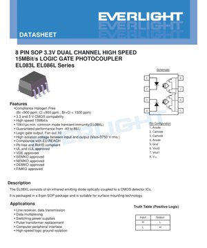
The EL08XL series represents a family of dual-channel, high-speed logic gate photocouplers (opto-isolators) designed for modern digital isolation applications. These devices integrate an infrared emitting diode optically coupled to a CMOS detector integrated circuit within a compact 8-pin Small Outline Package (SOP). The primary function is to provide galvanic isolation between input and output circuits while transmitting high-speed digital signals with minimal distortion.
The core advantage of this series lies in its combination of high-speed performance (up to 15 Megabits per second), compatibility with low-voltage 3.3V and 5V CMOS logic families, and robust isolation characteristics. The devices are engineered to replace pulse transformers and other isolation methods in demanding applications, offering a reliable, compact, and surface-mountable solution. Target markets include industrial automation, telecommunications, power supply control, computer peripherals, and any system requiring noise-immune data transmission across voltage domains.
2. Technical Parameter Deep Dive
2.1 Absolute Maximum Ratings
The device is specified for reliable operation within defined limits. Key absolute maximum ratings include: a forward current (IF) of 20 mA for the input LED, a reverse voltage (VR) of 5V, and power dissipation limits of 35 mW for the input and 85 mW for the output. The supply voltage (VCC) and output voltage (VO) must not exceed 5.5V. A critical parameter is the isolation voltage (VISO) of 3750 Vrms for one minute, tested under specific humidity conditions with input and output pins shorted separately. The operating temperature range is from -40°C to +85°C.
2.2 Electrical Characteristics
Detailed DC parameters ensure compatibility with system design. The input LED has a typical forward voltage (VF) of 1.4V at 8mA, with a maximum of 1.8V. The output characteristics are defined for both 3.3V and 5V supply operation. The high-level output voltage (VOH) is guaranteed to be within 1V of VCC (min) when sinking 4mA. The low-level output voltage (VOL) is typically 0.21V (3.3V) or 0.17V (5V) when sourcing 4mA with the input LED driven at 8mA, ensuring strong logic levels. The input threshold current (IFT) for a valid low output is typically 2.5 mA, with a maximum of 5 mA.
2.3 Switching Characteristics
This section defines the dynamic performance. Propagation delay times (tPHL and tPLH) are typically 38-41 ns for a 3.3V supply and 35-46 ns for a 5V supply, with a maximum of 60 ns under specified test conditions (IF=8mA, CL=15pF). Pulse width distortion (|tPHL – tPLH|), which impacts signal integrity, is typically 6-8 ns with a maximum of 30 ns. Output rise and fall times (tr, tf) are typically 5.5-6 ns. A key differentiator is the Common Mode Transient Immunity (CMTI). The EL086L variant guarantees a minimum of 10,000 V/µs for both high and low output states, while the EL083L guarantees 5,000 V/µs. This parameter is critical in noisy environments with fast-changing ground potentials.
3. Performance Curve Analysis
The datasheet references typical electro-optical characteristic curves. While specific graphs are not detailed in the provided text, such curves typically illustrate the relationship between forward current and forward voltage for the input LED, propagation delay versus temperature, and common-mode transient immunity performance. These curves are essential for designers to understand device behavior under non-standard conditions and to optimize the operating point for speed, power, and reliability.
4. Mechanical and Package Information
4.1 Package Dimensions
The device is housed in an 8-pin SOP package. The dimensional drawing provides critical measurements for PCB footprint design, including overall package length, width, height, lead pitch (typically 1.27mm), and lead dimensions. Adherence to these dimensions is necessary for proper soldering and mechanical fit.
4.2 Pin Configuration and Polarity
The pinout is as follows: Pin 1 (Anode 1), Pin 2 (Cathode 1), Pin 3 (Cathode 2), Pin 4 (Anode 2), Pin 5 (Ground), Pin 6 (VOUT2), Pin 7 (VOUT1), Pin 8 (VCC). This configuration supports two independent channels. Correct polarity connection for the input LEDs (Anode/Cathode) and the output supply (VCC/GND) is mandatory to prevent device damage.
4.3 Recommended PCB Pad Layout
A suggested surface-mount pad layout is provided. The note emphasizes that this is a reference design and should be modified based on specific PCB manufacturing processes and thermal requirements. The pad design aims to ensure reliable solder fillets and mechanical strength after reflow soldering.
5. Soldering and Assembly Guidelines
The absolute maximum ratings specify a soldering temperature (TSOL) of 260°C for 10 seconds. This aligns with typical lead-free reflow profiles. It is crucial to follow the recommended reflow profile for the specific PCB assembly to avoid thermal damage. The device must be stored under appropriate conditions (TSTG: -55°C to +125°C) before use to maintain solderability.
6. Application Suggestions
6.1 Typical Application Circuits
The primary applications listed are line receivers, data transmission systems, data multiplexing, switching power supply feedback isolation, pulse transformer replacement, computer peripheral interfaces, and high-speed logic ground isolation. In a typical circuit, the input side is driven by a logic signal through a current-limiting resistor to set IF. The output side requires a bypass capacitor (0.1µF or larger, with good high-frequency characteristics) connected as close as possible between the VCC and GND pins to ensure stable operation and minimize noise.
6.2 Design Considerations
- Power Supply Decoupling: The mandatory use of a local bypass capacitor on the output side is critical for achieving the specified high-speed performance and immunity to noise.
- Input Current Setting: The forward current (IF) should be set based on the required speed and the guaranteed IFT. Operating at the recommended 8mA ensures proper noise margin and switching speed.
- Load Considerations: The output can drive up to 10 standard CMOS loads. The datasheet specifies test conditions with IO = ±4mA for VOH/VOL.
- Channel Selection: Choose between EL083L (5kV/µs CMTI) and EL086L (10kV/µs CMTI) based on the electrical noise environment of the application.
7. Technical Comparison and Differentiation
The EL08XL series differentiates itself through its dual-channel design in a standard SOP-8 package, offering board space savings compared to two single-channel devices. The guaranteed 15Mbit/s speed at 3.3V/5V is a key performance marker for modern digital interfaces. The high Common Mode Transient Immunity, especially the 10kV/µs rating of the EL086L, provides superior performance in high-noise industrial and power conversion environments compared to standard optocouplers. Compliance with halogen-free, RoHS, REACH, and major international safety standards (UL, cUL, VDE, etc.) makes it suitable for global markets.
8. Frequently Asked Questions (Based on Technical Parameters)
Q: Can I use a 5V supply for the output if my logic is 3.3V?
A: The output stage is compatible with both 3.3V and 5V CMOS levels. However, you must ensure the receiving logic device is 5V tolerant if you use a 5V VCC. The VOH will be near 5V.
Q: What is the purpose of the CMTI specification?
A: CMTI measures the device's ability to reject fast voltage transients between the input and output grounds. A high CMTI (e.g., 10kV/µs) prevents these transients from causing erroneous output switching, which is vital in motor drives, power supplies, and industrial PLCs.
Q: How do I calculate the input series resistor?
A: Rseries = (Vdriver - VF) / IF. Use VF from the datasheet (max 1.8V) and choose IF (e.g., 8mA for full performance). Ensure the driver can source the required current.
Q: Is external pull-up/pull-down required on the output?
A: No. The output is an active CMOS push-pull stage, providing both sourcing and sinking current capability.
9. Practical Design Case
Scenario: Isolating a 3.3V UART (115200 baud) signal between a microcontroller on a noisy motor control board and a communication module on a clean logic board.
Implementation: Use one channel of an EL086L. On the microcontroller side, connect the TX pin via a 180Ω resistor (for ~8mA IF with a 3.3V driver) to the photocoupler input (Anode). Connect the cathode to ground. On the isolated side, power the VCC pin (Pin 8) with 3.3V from the communication module's supply. Place a 0.1µF ceramic capacitor directly between Pin 8 (VCC) and Pin 5 (GND). Connect the output (Pin 7, VOUT1) to the RX pin of the communication module. The high CMTI of the EL086L ensures data integrity despite ground noise from the motor driver.
10. Operating Principle
The device operates on the principle of optical isolation. An electrical current applied to the input infrared Light Emitting Diode (LED) causes it to emit light. This light traverses an optically transparent isolation barrier (typically a molded polymer). On the other side, a monolithic CMOS integrated circuit photodetector converts the received light intensity back into an electrical signal. This CMOS IC includes amplification, shaping, and a push-pull output stage to produce a clean digital waveform. The optical path provides the galvanic isolation, as there is no electrical connection between the input and output, only a light beam.
11. Industry Trends
The trend in digital isolation is towards higher speeds, lower power consumption, smaller packages, and higher integration. While traditional optocouplers like this series remain popular for their simplicity and high isolation voltage, alternative technologies based on capacitive (using SiO2 barriers) or magnetic (giant magnetoresistance) coupling are emerging. These can offer higher speeds, better timing accuracy, and longer lifetime as they have no LED to degrade. However, high-voltage optocouplers continue to dominate in applications requiring very high working isolation voltages (several kV) and proven reliability. The integration of additional functions like power delivery across the barrier (isolated DC-DC converters) or multiple channels with enhanced safety ratings is also a key development direction.
LED Specification Terminology
Complete explanation of LED technical terms
Photoelectric Performance
| Term | Unit/Representation | Simple Explanation | Why Important |
|---|---|---|---|
| Luminous Efficacy | lm/W (lumens per watt) | Light output per watt of electricity, higher means more energy efficient. | Directly determines energy efficiency grade and electricity cost. |
| Luminous Flux | lm (lumens) | Total light emitted by source, commonly called "brightness". | Determines if the light is bright enough. |
| Viewing Angle | ° (degrees), e.g., 120° | Angle where light intensity drops to half, determines beam width. | Affects illumination range and uniformity. |
| CCT (Color Temperature) | K (Kelvin), e.g., 2700K/6500K | Warmth/coolness of light, lower values yellowish/warm, higher whitish/cool. | Determines lighting atmosphere and suitable scenarios. |
| CRI / Ra | Unitless, 0–100 | Ability to render object colors accurately, Ra≥80 is good. | Affects color authenticity, used in high-demand places like malls, museums. |
| SDCM | MacAdam ellipse steps, e.g., "5-step" | Color consistency metric, smaller steps mean more consistent color. | Ensures uniform color across same batch of LEDs. |
| Dominant Wavelength | nm (nanometers), e.g., 620nm (red) | Wavelength corresponding to color of colored LEDs. | Determines hue of red, yellow, green monochrome LEDs. |
| Spectral Distribution | Wavelength vs intensity curve | Shows intensity distribution across wavelengths. | Affects color rendering and quality. |
Electrical Parameters
| Term | Symbol | Simple Explanation | Design Considerations |
|---|---|---|---|
| Forward Voltage | Vf | Minimum voltage to turn on LED, like "starting threshold". | Driver voltage must be ≥Vf, voltages add up for series LEDs. |
| Forward Current | If | Current value for normal LED operation. | Usually constant current drive, current determines brightness & lifespan. |
| Max Pulse Current | Ifp | Peak current tolerable for short periods, used for dimming or flashing. | Pulse width & duty cycle must be strictly controlled to avoid damage. |
| Reverse Voltage | Vr | Max reverse voltage LED can withstand, beyond may cause breakdown. | Circuit must prevent reverse connection or voltage spikes. |
| Thermal Resistance | Rth (°C/W) | Resistance to heat transfer from chip to solder, lower is better. | High thermal resistance requires stronger heat dissipation. |
| ESD Immunity | V (HBM), e.g., 1000V | Ability to withstand electrostatic discharge, higher means less vulnerable. | Anti-static measures needed in production, especially for sensitive LEDs. |
Thermal Management & Reliability
| Term | Key Metric | Simple Explanation | Impact |
|---|---|---|---|
| Junction Temperature | Tj (°C) | Actual operating temperature inside LED chip. | Every 10°C reduction may double lifespan; too high causes light decay, color shift. |
| Lumen Depreciation | L70 / L80 (hours) | Time for brightness to drop to 70% or 80% of initial. | Directly defines LED "service life". |
| Lumen Maintenance | % (e.g., 70%) | Percentage of brightness retained after time. | Indicates brightness retention over long-term use. |
| Color Shift | Δu′v′ or MacAdam ellipse | Degree of color change during use. | Affects color consistency in lighting scenes. |
| Thermal Aging | Material degradation | Deterioration due to long-term high temperature. | May cause brightness drop, color change, or open-circuit failure. |
Packaging & Materials
| Term | Common Types | Simple Explanation | Features & Applications |
|---|---|---|---|
| Package Type | EMC, PPA, Ceramic | Housing material protecting chip, providing optical/thermal interface. | EMC: good heat resistance, low cost; Ceramic: better heat dissipation, longer life. |
| Chip Structure | Front, Flip Chip | Chip electrode arrangement. | Flip chip: better heat dissipation, higher efficacy, for high-power. |
| Phosphor Coating | YAG, Silicate, Nitride | Covers blue chip, converts some to yellow/red, mixes to white. | Different phosphors affect efficacy, CCT, and CRI. |
| Lens/Optics | Flat, Microlens, TIR | Optical structure on surface controlling light distribution. | Determines viewing angle and light distribution curve. |
Quality Control & Binning
| Term | Binning Content | Simple Explanation | Purpose |
|---|---|---|---|
| Luminous Flux Bin | Code e.g., 2G, 2H | Grouped by brightness, each group has min/max lumen values. | Ensures uniform brightness in same batch. |
| Voltage Bin | Code e.g., 6W, 6X | Grouped by forward voltage range. | Facilitates driver matching, improves system efficiency. |
| Color Bin | 5-step MacAdam ellipse | Grouped by color coordinates, ensuring tight range. | Guarantees color consistency, avoids uneven color within fixture. |
| CCT Bin | 2700K, 3000K etc. | Grouped by CCT, each has corresponding coordinate range. | Meets different scene CCT requirements. |
Testing & Certification
| Term | Standard/Test | Simple Explanation | Significance |
|---|---|---|---|
| LM-80 | Lumen maintenance test | Long-term lighting at constant temperature, recording brightness decay. | Used to estimate LED life (with TM-21). |
| TM-21 | Life estimation standard | Estimates life under actual conditions based on LM-80 data. | Provides scientific life prediction. |
| IESNA | Illuminating Engineering Society | Covers optical, electrical, thermal test methods. | Industry-recognized test basis. |
| RoHS / REACH | Environmental certification | Ensures no harmful substances (lead, mercury). | Market access requirement internationally. |
| ENERGY STAR / DLC | Energy efficiency certification | Energy efficiency and performance certification for lighting. | Used in government procurement, subsidy programs, enhances competitiveness. |