1. Product Overview
The EL253X series comprises dual-channel, high-speed transistor photocouplers. Each device integrates an infrared emitting diode optically coupled to a high-speed photodetector transistor. A key architectural feature is the separate connection for the photodiode bias and the output-transistor collector. This design significantly enhances operational speed by reducing the base-collector capacitance of the input transistor compared to conventional phototransistor couplers. The devices are offered in a standard 8-pin Dual In-line Package (DIP) and are available with options for wide-lead spacing and surface-mount configurations.
1.1 Core Advantages and Target Market
The primary advantage of the EL253X series is its combination of high-speed data transmission capability (up to 1 Megabit per second) and robust electrical isolation. This makes it suitable for applications requiring reliable signal transfer between circuits with different ground potentials or voltage levels. Key features supporting this include a high common-mode transient immunity (CMTI) of 10kV/μs minimum for the EL2611 variant, ensuring stable operation in noisy electrical environments, and a high isolation voltage of 5000 Vrms between input and output. The devices are guaranteed to perform across a wide temperature range from -40°C to +85°C, catering to industrial and automotive applications. The logic gate output simplifies interface with digital circuits. Compliance with Pb-free and RoHS directives, along with approvals from major international safety agencies (UL, cUL, VDE, SEMKO, NEMKO, DEMKO, FIMKO), underscores their reliability and suitability for global markets. Target applications include line receivers, telecommunications equipment, isolation for power transistors in motor drives, feedback loops in switch-mode power supplies (SMPS), home appliances, and as upgrades for lower-speed phototransistor couplers.
2. In-Depth Technical Parameter Analysis
This section provides a detailed, objective interpretation of the electrical and performance characteristics specified in the datasheet.
2.1 Absolute Maximum Ratings
These ratings define the stress limits beyond which permanent damage to the device may occur. They are not recommended operating conditions. Critical limits include: a continuous forward current (I_F) of 25mA, a peak forward current (I_FP) of 50mA (50% duty cycle, 1ms pulse width), and a very high peak transient current (I_Ftrans) of 1A for very short pulses (≤1μs). The output can withstand a voltage (V_O) from -0.5V to 20V, and the supply voltage (V_CC) can range from -0.5V to 30V. The isolation voltage (V_ISO) is rated at 5000 Vrms for one minute, tested under specific humidity conditions. The device can be operated in ambient temperatures (T_OPR) from -40°C to +100°C and stored (T_STG) from -40°C to +125°C. The soldering temperature (T_SOL) is specified as 260°C for 10 seconds, which is a standard lead-free reflow profile.
2.2 Electrical Characteristics
These parameters define the device's performance under normal operating conditions, typically at 25°C unless otherwise noted.
2.2.1 Input Characteristics
The forward voltage (V_F) is typically 1.45V at a forward current (I_F) of 16mA. It has a negative temperature coefficient of approximately -1.9 mV/°C, meaning V_F decreases slightly as temperature increases. The maximum reverse voltage (V_R) is 5V. The input capacitance (C_IN) is typically 60pF, which is a factor in high-speed switching performance.
2.2.2 Output Characteristics
The logic high output current (I_OH) is very low (typ. 0.001µA at V_CC=5.5V), indicating excellent output leakage characteristics in the off-state. The supply current differs significantly between logic states: the logic low supply current (I_CCL) is typically 140µA when the input LED is driven (I_F=16mA), while the logic high supply current (I_CCH) is typically only 0.01µA when the input is off. This highlights the low power consumption in the idle state.
2.3 Transfer Characteristics
This defines the relationship between input and output.
2.3.1 Current Transfer Ratio (CTR)
The CTR, a key parameter for photocouplers, is the ratio of output collector current to input LED current, expressed as a percentage. The EL2530 has a CTR range of 7% to 50%, while the EL2531 has a higher range of 19% to 50% (both at I_F=16mA, V_O=0.4V, V_CC=4.5V, 25°C). The EL2531 is therefore the higher-gain variant. Minimum CTR values are guaranteed at 5% for EL2530 and 15% for EL2531 under slightly different conditions (V_O=0.5V).
2.3.2 Logic Low Output Voltage (V_OL)
This is the voltage at the output when the device is in the 'on' or low state. For the EL2530, V_OL is typically 0.18V with an output current (I_O) of 1.1mA. For the EL2531, it is typically 0.25V with I_O=3mA. The maximum V_OL for both is 0.5V under their respective test conditions, ensuring solid logic-low levels for interfacing.
2.4 Switching Characteristics
These parameters are critical for high-speed applications. Tests are conducted at I_F=16mA and V_CC=5V.
2.4.1 Propagation Delay
Propagation delay to logic low (t_PHL) and to logic high (t_PLH) are measured. For the EL2530 with a 4.1kΩ load resistor (R_L), t_PHL is typically 0.35µs (max 2.0µs) and t_PLH is typically 0.5µs (max 2.0µs). For the EL2531 with a 1.9kΩ R_L, both delays are typically 0.35µs and 0.3µs respectively (max 1.0µs). The EL2531 demonstrates faster switching times, partly due to its higher CTR allowing the use of a smaller pull-up resistor.
2.4.2 Common Mode Transient Immunity (CMTI)
CMTI measures the device's ability to reject fast voltage transients between the input and output grounds. It is specified in Volts per microsecond (V/µs). Both EL2530 and EL2531 have a minimum CMTI of 1000 V/µs and a typical value of 10,000 V/µs for both logic high (CM_H) and logic low (CM_L) states. The test conditions differ: EL2530 uses a 10V p-p common-mode pulse, while EL2531 uses a 1000V p-p pulse, indicating potentially more robust testing for the latter variant in this aspect.
3. Performance Curve Analysis
The datasheet references typical electro-optical characteristic curves. While the specific graphs are not reproduced in the provided text, they typically include plots of Current Transfer Ratio (CTR) vs. Forward Current (I_F), CTR vs. Ambient Temperature (T_A), Propagation Delay vs. Load Resistance (R_L), and Forward Voltage (V_F) vs. I_F. These curves are essential for designers to understand how parameters shift under non-ideal or varying conditions, such as lower drive currents, higher temperatures, or different load configurations, allowing for robust circuit design across the specified operating range.
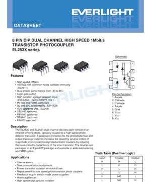
4. Mechanical and Package Information
The device uses an 8-pin DIP package. The pin configuration is as follows: Pin 1: Anode (Channel 1), Pin 2: Cathode (Channel 1), Pin 3: Cathode (Channel 2), Pin 4: Anode (Channel 2), Pin 5: Ground (GND), Pin 6: Output 2 (V_OUT2), Pin 7: Output 1 (V_OUT1), Pin 8: Supply Voltage (V_CC). The package is available in several lead form options: standard DIP, wide-lead bend (0.4-inch spacing, option 'M'), and surface-mount lead forms (options 'S' and low-profile 'S1').
5. Soldering and Assembly Guidelines
The absolute maximum rating for soldering temperature is 260°C for 10 seconds. This aligns with typical lead-free reflow soldering profiles. For wave soldering or hand soldering, standard practices for through-hole or SMD components should be followed, respecting the maximum temperature and time limits to prevent package damage or degradation of internal materials. Devices should be stored in conditions within the storage temperature range (-40°C to +125°C) and in moisture-sensitive packaging if applicable for SMD variants to prevent 'popcorning' during reflow.
6. Packaging and Ordering Information
The part number follows the format: EL253XY(Z)-V. 'X' denotes the part number (0 for EL2530, 1 for EL2531). 'Y' indicates the lead form option: blank for standard DIP, 'M' for wide lead bend, 'S' for surface mount, 'S1' for low-profile surface mount. 'Z' specifies the tape and reel option: 'TA' or 'TB' (different reel types), or blank for tube packaging. 'V' is an optional suffix for VDE approval. Packing quantities are 45 units per tube for through-hole versions and 1000 units per reel for tape-and-reel SMD versions.
7. Application Recommendations
7.1 Typical Application Scenarios
- Line Receivers: Isolating digital communication lines (e.g., RS-485, RS-422) to prevent ground loops and noise.
- Motor Drive Isolation: Providing gate drive signals to power transistors (IGBTs, MOSFETs) in variable frequency drives, isolating the low-voltage control logic from the high-voltage power stage.
- Switch-Mode Power Supply (SMPS) Feedback: Isolating the feedback error signal from the secondary (output) side to the primary (input) side controller, a critical safety and functional requirement.
- Logic Ground Isolation: Separating grounds between noisy digital subsystems (e.g., between a microcontroller and a motor driver IC) to prevent noise coupling.
- Telecom Equipment: Signal isolation in ringing circuits, line interfaces, or data line protection.
7.2 Design Considerations
- Current Limiting Resistor: An external resistor must be used in series with the input LED to set the forward current (I_F), typically to the recommended 16mA for optimal speed and CTR.
- Pull-Up Resistor: The output requires a pull-up resistor (R_L) to V_CC. Its value affects switching speed and power consumption. The datasheet specifies test conditions with 4.1kΩ for EL2530 and 1.9kΩ for EL2531.
- Power Supply Decoupling: Place a bypass capacitor (e.g., 0.1µF) close to the V_CC pin (Pin 8) and ground to ensure stable operation and minimize switching noise.
- Layout for High CMTI: To maintain the high CMTI, minimize the parasitic capacitance between the input and output sections of the PCB layout. Provide adequate creepage and clearance distances as per safety standards.
- Choosing EL2530 vs. EL2531: Select EL2531 for applications requiring faster switching speeds or where a lower-value pull-up resistor is acceptable. EL2530 may be chosen for applications with less stringent speed requirements or where lower supply current in the on-state (due to higher R_L) is a priority.
8. Technical Comparison and Differentiation
The EL253X series differentiates itself from standard phototransistor couplers primarily through its high speed (1Mbit/s vs. typically <100kbit/s for standard types). The separate photodiode bias connection is the key architectural difference enabling this. Compared to other high-speed optocouplers (like those with integrated logic gates or higher-speed digital isolators), the EL253X offers a simple, robust transistor output, which can be advantageous in certain analog or level-shifting applications, and typically comes at a lower cost. Its dual-channel configuration in a single 8-pin package saves board space compared to using two single-channel devices.
9. Frequently Asked Questions (Based on Technical Parameters)
Q: What is the main difference between EL2530 and EL2531?
A: The primary difference is the guaranteed minimum Current Transfer Ratio (CTR). EL2531 has a higher minimum CTR (15-19% depending on test condition) compared to EL2530 (5-7%). This generally allows the EL2531 to switch faster with a given load resistor or to use a larger pull-up resistor for the same speed, affecting power consumption and drive capability.
Q: Can I drive the input LED with a voltage source directly?
A: No. The LED must be driven with a current-limited source, typically implemented with a series resistor from a voltage supply. The datasheet provides forward voltage (V_F) characteristics to help calculate the appropriate resistor value for the desired I_F (e.g., 16mA).
Q: What does a Common Mode Transient Immunity (CMTI) of 10kV/µs mean?
A: It means the output state will remain correct (not falsely toggle) even if the voltage difference between the input and output circuit grounds changes at a rate as high as 10,000 volts per microsecond. This is crucial in motor drives or power supplies where fast high-voltage switching creates large ground transients.
Q: Is a heatsink required?
A: Under normal operating conditions within the absolute maximum ratings for power dissipation (P_IN=45mW, P_O=35mW), a heatsink is not required. The power dissipated is relatively low. Proper PCB layout for thermal dissipation is usually sufficient.
10. Practical Design and Usage Examples
Case 1: Isolated GPIO Expander. A microcontroller needs to monitor 12V limit switches in an industrial panel. Using six EL2531 channels, the microcontroller's 3.3V GPIOs can drive the LEDs via current-limiting resistors. The outputs, pulled up to 12V, provide a clean logic signal to the switches. The 5000Vrms isolation protects the microcontroller from potential transients on the 12V industrial lines.
Case 2: Gate Driver for a Half-Bridge MOSFET. In a low-power DC motor controller, a single EL2531 channel can be used to drive the high-side MOSFET. The input is driven by the PWM signal from the controller. The output, connected to the MOSFET gate via a suitable gate resistor and pulled up to a bootstrap supply, provides the isolated gate drive. The high CMTI ensures the gate signal remains stable during the rapid switching of the half-bridge.
11. Operating Principle
The fundamental principle is opto-electronic conversion. An electrical current applied to the input Infrared Emitting Diode (IRED) causes it to emit light. This light traverses an optically transparent but electrically insulating barrier (typically silicone or similar material). The light strikes the photodiode of the integrated detector, generating a photocurrent. In the EL253X, this photocurrent directly biases the base of the output NPN transistor, turning it on and pulling the output pin (collector) low. The separate connection for the photodiode allows the photocurrent to be used more efficiently for switching, rather than being partially shunted by the transistor's base-collector capacitance, which is the speed-limiting factor in traditional phototransistors.
12. Technology Trends
The field of signal isolation is evolving. While transistor-output photocouplers like the EL253X remain highly relevant for their simplicity, robustness, and cost-effectiveness, several trends are notable. There is a move towards higher integration, such as devices with integrated drivers for IGBTs/GaN FETs. Digital isolators based on CMOS technology and RF or capacitive coupling offer significantly higher data rates (tens to hundreds of Mbps), lower power consumption, and higher reliability (no LED aging). However, photocouplers maintain advantages in certain areas: very high isolation voltage capability, excellent common-mode transient immunity, and inherent immunity to magnetic fields. The development focus for photocouplers includes improving speed further, reducing package size (especially for SMD), enhancing high-temperature performance, and increasing reliability metrics like long-term CTR stability.
LED Specification Terminology
Complete explanation of LED technical terms
Photoelectric Performance
| Term | Unit/Representation | Simple Explanation | Why Important |
|---|---|---|---|
| Luminous Efficacy | lm/W (lumens per watt) | Light output per watt of electricity, higher means more energy efficient. | Directly determines energy efficiency grade and electricity cost. |
| Luminous Flux | lm (lumens) | Total light emitted by source, commonly called "brightness". | Determines if the light is bright enough. |
| Viewing Angle | ° (degrees), e.g., 120° | Angle where light intensity drops to half, determines beam width. | Affects illumination range and uniformity. |
| CCT (Color Temperature) | K (Kelvin), e.g., 2700K/6500K | Warmth/coolness of light, lower values yellowish/warm, higher whitish/cool. | Determines lighting atmosphere and suitable scenarios. |
| CRI / Ra | Unitless, 0–100 | Ability to render object colors accurately, Ra≥80 is good. | Affects color authenticity, used in high-demand places like malls, museums. |
| SDCM | MacAdam ellipse steps, e.g., "5-step" | Color consistency metric, smaller steps mean more consistent color. | Ensures uniform color across same batch of LEDs. |
| Dominant Wavelength | nm (nanometers), e.g., 620nm (red) | Wavelength corresponding to color of colored LEDs. | Determines hue of red, yellow, green monochrome LEDs. |
| Spectral Distribution | Wavelength vs intensity curve | Shows intensity distribution across wavelengths. | Affects color rendering and quality. |
Electrical Parameters
| Term | Symbol | Simple Explanation | Design Considerations |
|---|---|---|---|
| Forward Voltage | Vf | Minimum voltage to turn on LED, like "starting threshold". | Driver voltage must be ≥Vf, voltages add up for series LEDs. |
| Forward Current | If | Current value for normal LED operation. | Usually constant current drive, current determines brightness & lifespan. |
| Max Pulse Current | Ifp | Peak current tolerable for short periods, used for dimming or flashing. | Pulse width & duty cycle must be strictly controlled to avoid damage. |
| Reverse Voltage | Vr | Max reverse voltage LED can withstand, beyond may cause breakdown. | Circuit must prevent reverse connection or voltage spikes. |
| Thermal Resistance | Rth (°C/W) | Resistance to heat transfer from chip to solder, lower is better. | High thermal resistance requires stronger heat dissipation. |
| ESD Immunity | V (HBM), e.g., 1000V | Ability to withstand electrostatic discharge, higher means less vulnerable. | Anti-static measures needed in production, especially for sensitive LEDs. |
Thermal Management & Reliability
| Term | Key Metric | Simple Explanation | Impact |
|---|---|---|---|
| Junction Temperature | Tj (°C) | Actual operating temperature inside LED chip. | Every 10°C reduction may double lifespan; too high causes light decay, color shift. |
| Lumen Depreciation | L70 / L80 (hours) | Time for brightness to drop to 70% or 80% of initial. | Directly defines LED "service life". |
| Lumen Maintenance | % (e.g., 70%) | Percentage of brightness retained after time. | Indicates brightness retention over long-term use. |
| Color Shift | Δu′v′ or MacAdam ellipse | Degree of color change during use. | Affects color consistency in lighting scenes. |
| Thermal Aging | Material degradation | Deterioration due to long-term high temperature. | May cause brightness drop, color change, or open-circuit failure. |
Packaging & Materials
| Term | Common Types | Simple Explanation | Features & Applications |
|---|---|---|---|
| Package Type | EMC, PPA, Ceramic | Housing material protecting chip, providing optical/thermal interface. | EMC: good heat resistance, low cost; Ceramic: better heat dissipation, longer life. |
| Chip Structure | Front, Flip Chip | Chip electrode arrangement. | Flip chip: better heat dissipation, higher efficacy, for high-power. |
| Phosphor Coating | YAG, Silicate, Nitride | Covers blue chip, converts some to yellow/red, mixes to white. | Different phosphors affect efficacy, CCT, and CRI. |
| Lens/Optics | Flat, Microlens, TIR | Optical structure on surface controlling light distribution. | Determines viewing angle and light distribution curve. |
Quality Control & Binning
| Term | Binning Content | Simple Explanation | Purpose |
|---|---|---|---|
| Luminous Flux Bin | Code e.g., 2G, 2H | Grouped by brightness, each group has min/max lumen values. | Ensures uniform brightness in same batch. |
| Voltage Bin | Code e.g., 6W, 6X | Grouped by forward voltage range. | Facilitates driver matching, improves system efficiency. |
| Color Bin | 5-step MacAdam ellipse | Grouped by color coordinates, ensuring tight range. | Guarantees color consistency, avoids uneven color within fixture. |
| CCT Bin | 2700K, 3000K etc. | Grouped by CCT, each has corresponding coordinate range. | Meets different scene CCT requirements. |
Testing & Certification
| Term | Standard/Test | Simple Explanation | Significance |
|---|---|---|---|
| LM-80 | Lumen maintenance test | Long-term lighting at constant temperature, recording brightness decay. | Used to estimate LED life (with TM-21). |
| TM-21 | Life estimation standard | Estimates life under actual conditions based on LM-80 data. | Provides scientific life prediction. |
| IESNA | Illuminating Engineering Society | Covers optical, electrical, thermal test methods. | Industry-recognized test basis. |
| RoHS / REACH | Environmental certification | Ensures no harmful substances (lead, mercury). | Market access requirement internationally. |
| ENERGY STAR / DLC | Energy efficiency certification | Energy efficiency and performance certification for lighting. | Used in government procurement, subsidy programs, enhances competitiveness. |