Table of Contents
- 1. Product Overview
- 2. Technical Parameter Deep Dive
- 2.1 Absolute Maximum Ratings
- 2.2 Electrical & Transfer Characteristics
- 2.3 Switching Characteristics
- 3. Performance Curve Analysis
- 4. Mechanical & Package Information
- 5. Soldering & Assembly Guidelines
- 6. Packaging & Ordering Information
- 7. Application Suggestions
- 7.1 Typical Application Circuits
- 7.2 Design Considerations
- 8. Technical Comparison & Advantages
- 9. Frequently Asked Questions (FAQ)
- 10. Design & Usage Case Study
- 11. Operating Principle
- 12. Technology Trends
- LED Specification Terminology
- Photoelectric Performance
- Electrical Parameters
- Thermal Management & Reliability
- Packaging & Materials
- Quality Control & Binning
- Testing & Certification
1. Product Overview
The EL053X series represents a family of dual-channel, high-speed transistor photocouplers designed for reliable signal isolation in demanding electronic applications. Each device integrates an infrared emitting diode optically coupled to a high-speed photodetector transistor within a compact 8-pin Small Outline Package (SOP). The primary function is to provide electrical isolation between input and output circuits, preventing ground loops, noise transmission, and high-voltage surges from damaging sensitive components.
The core advantage of this series lies in its architecture. By providing separate connections for the photodiode bias and the output transistor's collector, the base-collector capacitance of the input transistor is significantly reduced. This design innovation increases the switching speed by several orders of magnitude compared to conventional phototransistor couplers, enabling reliable data transmission at rates up to 1 Megabit per second (1Mbit/s).
The target market for the EL053X includes industrial automation, telecommunications, power supply design, and motor control systems where noise immunity, safety isolation, and fast signal transmission are critical requirements.
2. Technical Parameter Deep Dive
2.1 Absolute Maximum Ratings
These ratings define the stress limits beyond which permanent damage to the device may occur. Operating the device continuously at or near these limits is not recommended.
- Input Forward Current (IF): 25 mA (continuous). This is the maximum steady-state current that can be driven through the input LED.
- Peak Forward Current (IFP): 50 mA. This higher current is permissible under pulsed conditions (50% duty cycle, 1ms pulse width) for brief periods.
- Reverse Voltage (VR): 5 V. The maximum voltage that can be applied in reverse bias across the input LED.
- Output Voltage (VO): -0.5 to 20 V. The allowable voltage range on the output collector pin relative to the emitter (ground).
- Supply Voltage (VCC): -0.5 to 30 V. The voltage supplied to the photodiode bias pin (Pin 8).
- Isolation Voltage (VISO): 3750 Vrms. This is a critical safety parameter. It indicates the maximum AC voltage (applied for 1 minute) that can be sustained between the input side (pins 1-4) and the output side (pins 5-8) without breakdown, ensuring user safety and system integrity.
- Operating Temperature (TOPR): -55°C to +100°C. The ambient temperature range over which the device is guaranteed to function, though some electrical parameters are specified from 0°C to 70°C.
2.2 Electrical & Transfer Characteristics
These parameters define the device's performance under normal operating conditions (Ta=0°C to 70°C unless noted).
Input Characteristics:
- Forward Voltage (VF): Typically 1.4V at a forward current (IF) of 16mA, with a maximum of 1.8V. This is used to calculate the required current-limiting resistor for the input side.
- Temperature Coefficient (ΔVF/ΔTA): Approximately -1.6 mV/°C. The LED's forward voltage decreases as temperature increases, which is a typical characteristic of semiconductor diodes.
Output & Transfer Characteristics: The series includes two part number variants, EL0530 and EL0531, which differ primarily in their Current Transfer Ratio (CTR).
- Current Transfer Ratio (CTR): This is the ratio of the output transistor's collector current to the input LED's forward current, expressed as a percentage. It is a measure of the device's sensitivity.
- EL0530: CTR min. 7%, typ. up to 50% at 25°C.
- EL0531: CTR min. 19%, typ. up to 50% at 25°C.
- Logic Low Output Voltage (VOL): The voltage at the output when the device is in the \"on\" state (LED energized). For example, the EL0531 has a typical VOL of 0.3V and a maximum of 0.4V when IF=16mA and IO=3mA. A low VOL is essential for clean logic-low signaling.
- Supply Currents (ICCL, ICCH): ICCL is the current drawn by the VCC pin when the input LED is on (typ. 120µA). ICCH is the current when the LED is off (typ. 0.01µA). These are important for calculating the total power consumption of the isolation stage.
2.3 Switching Characteristics
These parameters define the speed performance, measured under standard test conditions (IF=16mA, Vcc=5V).
- Propagation Delay (tPHL, tPLH): The time delay between the input signal edge and the corresponding output response.
- EL0530: Maximum 2.0 µs (with RL=4.1kΩ).
- EL0531: Maximum 1.0 µs (with RL=1.9kΩ).
- Common Mode Transient Immunity (CMH, CML): This is a crucial parameter for noise immunity in isolated systems. It measures the maximum rate of change (dV/dt) of a voltage spike that appears equally on both sides of the isolation barrier that the device can tolerate without causing an erroneous output glitch.
- For the EL0531, the minimum guaranteed immunity is 1000 V/µs for both high and low output states when subjected to common-mode pulses (VCM). High CMTI values (10,000 V/µs typical for EL0530) ensure reliable operation in noisy environments like motor drives or switch-mode power supplies.
- Current Transfer Ratio (CTR) vs. Forward Current (IF): Shows how sensitivity changes with drive current. CTR often decreases slightly at very high IF.
- CTR vs. Ambient Temperature (TA): Illustrates the temperature dependence of the device's sensitivity. CTR generally decreases as temperature increases.
- Propagation Delay vs. Load Resistor (RL): Demonstrates the trade-off between switching speed and power consumption; smaller RL gives faster speed but higher output current.
- Forward Voltage (VF) vs. Forward Current (IF): The standard diode IV curve for the input LED.
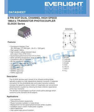
- Anode (Channel 1 Input)
- Cathode (Channel 1 Input) <3>Cathode (Channel 2 Input)<4>Anode (Channel 2 Input)<5>Ground (GND) - Output side common<6>Vout 2 (Channel 2 Output Collector)<7>Vout 1 (Channel 1 Output Collector)<8>VCC (Photodiode Bias Supply)
- Tube Packaging: 100 units per tube. Options are standard (no suffix) or standard with VDE approval (\"-V\" suffix).
- Tape and Reel Packaging: 2000 units per reel. Designed for high-volume automated assembly. Two reel option codes are available: TA and TB. These can also be combined with the VDE option (e.g., \"(TA)-V\").
- Input Current Limiting: An external resistor must be connected in series with the input LED to set the forward current (IF). The value is calculated based on the supply voltage, the LED's forward voltage (VF ~1.4V), and the desired IF (e.g., 16mA for rated performance).
- Output Pull-Up Resistor: A resistor (RL) is required between the output collector (Vout) and the output supply voltage. Its value affects both switching speed (smaller RL = faster) and power consumption (smaller RL = higher current). The datasheet provides test conditions (RL=4.1kΩ for EL0530, 1.9kΩ for EL0531) that guarantee the specified propagation delays.
- Bypass Capacitor: A small ceramic capacitor (e.g., 0.1µF) should be placed close to the VCC pin (8) and GND pin (5) to stabilize the bias supply for the internal photodiode and minimize noise.
- Noise Immunity: To maximize the benefit of the high CMTI, ensure a clean layout. Minimize the parasitic capacitance between the input and output sides of the isolation barrier on the PCB. Keep the traces to the input and output pins short.
- Higher Speeds: Demand for faster data isolation in industrial Ethernet, servo drives, and advanced power supplies is pushing speeds beyond 10 Mbit/s and even into the 100 Mbit/s range, often using more advanced architectures like digital isolators or specialized high-speed couplers.
- Higher Integration: Integration of multiple channels (like the dual-channel EL053X), and even combining isolation with other functions like gate drivers or ADC interfaces in a single package.
- Improved Reliability & Lifetime: Focus on longer operational lifetime, especially for LED degradation, and higher reliability metrics like FIT rates for automotive and industrial applications.
- Miniaturization: Development of smaller package footprints while maintaining or improving isolation ratings to save PCB space in compact designs.
- Enhanced Safety Standards: Compliance with increasingly stringent international safety standards (UL, VDE, CQC) and environmental regulations (RoHS, REACH) remains a fundamental requirement.
3. Performance Curve Analysis
The datasheet references \"Typical Electro-Optical Characteristics Curves.\" While the specific graphs are not provided in the text excerpt, such curves typically include:
These curves are essential for designers to optimize performance across the intended operating temperature and current ranges.
4. Mechanical & Package Information
The device is housed in a standard 8-pin Small Outline Package (SOP). This surface-mount package conforms to the common SO-8 footprint, making it compatible with standard PCB layouts and automated assembly processes. The pin configuration is as follows:
Detailed mechanical drawings specifying package dimensions, pin spacing, and recommended PCB land pattern (footprint) are typically included in the full datasheet but are not present in the provided text.
5. Soldering & Assembly Guidelines
The Absolute Maximum Ratings specify a soldering temperature (TSOL) of 260°C for 10 seconds. This refers to the peak temperature experienced by the device body during reflow soldering processes. Designers must ensure their reflow profile complies with this limit to prevent package damage or degradation of internal bonds. Standard IPC/JEDEC guidelines for surface-mount devices should be followed for handling, moisture sensitivity (if applicable), and storage.
6. Packaging & Ordering Information
The EL053X series offers flexible packaging options to suit different production scales:
Part Numbering Rule: EL053X(Z)-V
Where:
- X = Part number variant (0 for EL0530, 1 for EL0531).
- Z = Tape and reel option (TA, TB, or omitted for tube).
- V = Optional VDE approval marking (included if \"-V\" is present).
7. Application Suggestions
7.1 Typical Application Circuits
Line Receivers & Logic Isolation: The high speed and good CMTI make the EL053X ideal for isolating digital communication lines (e.g., RS-485, CAN, SPI) in industrial networks to break ground loops and protect controllers from transients.
Feedback in Switch-Mode Power Supplies (SMPS): Used to transfer the feedback error signal from the secondary (output) side to the primary-side controller across the isolation barrier, a key requirement in isolated converters.
Gate Drive Isolation for Motor Drives: Provides isolated signal paths to drive the high-side and low-side power transistors (IGBTs/MOSFETs) in motor inverter bridges, ensuring safe and reliable operation.
Replacement for Low-Speed Phototransistor Couplers: Offers a direct upgrade path in existing designs requiring higher data rates or better noise immunity.
7.2 Design Considerations
8. Technical Comparison & Advantages
The EL053X series differentiates itself from standard phototransistor couplers through its dedicated speed-optimized architecture. Traditional phototransistor couplers have the phototransistor's base terminal unconnected, leading to high base-collector capacitance which severely limits bandwidth (often to below 100 kHz). By bringing out the photodiode bias separately, the EL053X effectively uses the photodiode in a photovoltaic mode to drive the transistor base with low impedance, drastically reducing the Miller capacitance effect and enabling operation at 1Mbit/s.
Compared to more complex and expensive digital isolators (which use CMOS technology and RF modulation), the EL053X offers a robust, analog solution with high intrinsic noise immunity, simplicity, and proven reliability in high-voltage environments, often at a lower cost for applications where its speed is sufficient.
9. Frequently Asked Questions (FAQ)
Q1: What is the main difference between EL0530 and EL0531?
A1: The primary difference is the guaranteed minimum Current Transfer Ratio (CTR). EL0531 has a higher minimum CTR (19% vs. 7%), making it more sensitive. This may allow the use of a slightly higher pull-up resistor (RL) for the same output current, potentially saving power, or it provides more design margin. The switching speed specifications are also tested with different RL values accordingly.
Q2: Can I operate the device at the full 100°C ambient temperature?
A2: The operating temperature range is -55°C to +100°C. However, the electrical characteristics tables are specified for 0°C to 70°C. For operation up to 100°C, you must consult the typical performance curves (like CTR vs. Temperature) to derate the parameters, as performance (like CTR and speed) will degrade at higher temperatures. The device will still function, but with reduced margins.
Q3: How do I ensure good Common Mode Transient Immunity in my design?
A3: First, choose a part with a high CMTI specification like the EL053X. Second, implement good PCB layout practices: minimize the overlap and parallel routing of traces on opposite sides of the isolation barrier, create a clear isolation gap on the PCB (typically >8mm for 3750Vrms), and use guard rings or isolation trenches if necessary. Proper bypassing of the VCC pin is also critical.
Q4: Is an external base resistor needed for the output transistor?
A4: No. Unlike a discrete phototransistor, the internal connection between the photodiode and the transistor base is optimized within the package. You only need to provide the VCC bias and the external collector pull-up resistor (RL).
10. Design & Usage Case Study
Scenario: Isolated SPI Communication for a Sensor Module.
A sensor is located in a high-noise motor environment (with 24V logic) and needs to communicate with a central 3.3V microcontroller located 2 meters away. Ground potential differences and motor noise are concerns.
Solution: Use two channels of an EL0531 device. The SPI clock (SCK) and Master-Out-Slave-In (MOSI) lines from the microcontroller (3.3V side) drive the input LEDs of two couplers via current-limiting resistors. The outputs, pulled up to 3.3V on the sensor board side, recreate the signals for the sensor's SPI interface. Similarly, the sensor's MISO line is sent back through another coupler channel. The 3750Vrms isolation breaks the ground connection between the two boards, eliminating ground loops. The 1Mbit/s speed is sufficient for most sensor data rates, and the high CMTI ensures the SPI communication is not corrupted by motor switching noise coupled as common-mode transients.
11. Operating Principle
The EL053X operates on the principle of optoelectronic conversion and isolation. When a current flows through the input Infrared Emitting Diode (IRED), it emits light proportional to the current. This light crosses a transparent isolation barrier (typically made of mold compound or silica) and strikes the photosensitive area of a silicon photodiode. The photodiode generates a current. This photocurrent is used to directly bias the base of an integrated NPN transistor. When the IRED is on, the photocurrent turns the transistor on, pulling the output collector (Vout) low towards the emitter (GND). When the IRED is off, no photocurrent flows, the transistor turns off, and the external pull-up resistor pulls Vout high to VCC (or the logic supply). The electrical connection is thus replaced by a light beam, providing the isolation.
12. Technology Trends
The market for optocouplers continues to evolve. Key trends include:
Devices like the EL053X series occupy a vital niche, offering an optimal balance of speed, cost, noise immunity, and reliability for a wide range of mainstream industrial and power applications.
LED Specification Terminology
Complete explanation of LED technical terms
Photoelectric Performance
| Term | Unit/Representation | Simple Explanation | Why Important |
|---|---|---|---|
| Luminous Efficacy | lm/W (lumens per watt) | Light output per watt of electricity, higher means more energy efficient. | Directly determines energy efficiency grade and electricity cost. |
| Luminous Flux | lm (lumens) | Total light emitted by source, commonly called "brightness". | Determines if the light is bright enough. |
| Viewing Angle | ° (degrees), e.g., 120° | Angle where light intensity drops to half, determines beam width. | Affects illumination range and uniformity. |
| CCT (Color Temperature) | K (Kelvin), e.g., 2700K/6500K | Warmth/coolness of light, lower values yellowish/warm, higher whitish/cool. | Determines lighting atmosphere and suitable scenarios. |
| CRI / Ra | Unitless, 0–100 | Ability to render object colors accurately, Ra≥80 is good. | Affects color authenticity, used in high-demand places like malls, museums. |
| SDCM | MacAdam ellipse steps, e.g., "5-step" | Color consistency metric, smaller steps mean more consistent color. | Ensures uniform color across same batch of LEDs. |
| Dominant Wavelength | nm (nanometers), e.g., 620nm (red) | Wavelength corresponding to color of colored LEDs. | Determines hue of red, yellow, green monochrome LEDs. |
| Spectral Distribution | Wavelength vs intensity curve | Shows intensity distribution across wavelengths. | Affects color rendering and quality. |
Electrical Parameters
| Term | Symbol | Simple Explanation | Design Considerations |
|---|---|---|---|
| Forward Voltage | Vf | Minimum voltage to turn on LED, like "starting threshold". | Driver voltage must be ≥Vf, voltages add up for series LEDs. |
| Forward Current | If | Current value for normal LED operation. | Usually constant current drive, current determines brightness & lifespan. |
| Max Pulse Current | Ifp | Peak current tolerable for short periods, used for dimming or flashing. | Pulse width & duty cycle must be strictly controlled to avoid damage. |
| Reverse Voltage | Vr | Max reverse voltage LED can withstand, beyond may cause breakdown. | Circuit must prevent reverse connection or voltage spikes. |
| Thermal Resistance | Rth (°C/W) | Resistance to heat transfer from chip to solder, lower is better. | High thermal resistance requires stronger heat dissipation. |
| ESD Immunity | V (HBM), e.g., 1000V | Ability to withstand electrostatic discharge, higher means less vulnerable. | Anti-static measures needed in production, especially for sensitive LEDs. |
Thermal Management & Reliability
| Term | Key Metric | Simple Explanation | Impact |
|---|---|---|---|
| Junction Temperature | Tj (°C) | Actual operating temperature inside LED chip. | Every 10°C reduction may double lifespan; too high causes light decay, color shift. |
| Lumen Depreciation | L70 / L80 (hours) | Time for brightness to drop to 70% or 80% of initial. | Directly defines LED "service life". |
| Lumen Maintenance | % (e.g., 70%) | Percentage of brightness retained after time. | Indicates brightness retention over long-term use. |
| Color Shift | Δu′v′ or MacAdam ellipse | Degree of color change during use. | Affects color consistency in lighting scenes. |
| Thermal Aging | Material degradation | Deterioration due to long-term high temperature. | May cause brightness drop, color change, or open-circuit failure. |
Packaging & Materials
| Term | Common Types | Simple Explanation | Features & Applications |
|---|---|---|---|
| Package Type | EMC, PPA, Ceramic | Housing material protecting chip, providing optical/thermal interface. | EMC: good heat resistance, low cost; Ceramic: better heat dissipation, longer life. |
| Chip Structure | Front, Flip Chip | Chip electrode arrangement. | Flip chip: better heat dissipation, higher efficacy, for high-power. |
| Phosphor Coating | YAG, Silicate, Nitride | Covers blue chip, converts some to yellow/red, mixes to white. | Different phosphors affect efficacy, CCT, and CRI. |
| Lens/Optics | Flat, Microlens, TIR | Optical structure on surface controlling light distribution. | Determines viewing angle and light distribution curve. |
Quality Control & Binning
| Term | Binning Content | Simple Explanation | Purpose |
|---|---|---|---|
| Luminous Flux Bin | Code e.g., 2G, 2H | Grouped by brightness, each group has min/max lumen values. | Ensures uniform brightness in same batch. |
| Voltage Bin | Code e.g., 6W, 6X | Grouped by forward voltage range. | Facilitates driver matching, improves system efficiency. |
| Color Bin | 5-step MacAdam ellipse | Grouped by color coordinates, ensuring tight range. | Guarantees color consistency, avoids uneven color within fixture. |
| CCT Bin | 2700K, 3000K etc. | Grouped by CCT, each has corresponding coordinate range. | Meets different scene CCT requirements. |
Testing & Certification
| Term | Standard/Test | Simple Explanation | Significance |
|---|---|---|---|
| LM-80 | Lumen maintenance test | Long-term lighting at constant temperature, recording brightness decay. | Used to estimate LED life (with TM-21). |
| TM-21 | Life estimation standard | Estimates life under actual conditions based on LM-80 data. | Provides scientific life prediction. |
| IESNA | Illuminating Engineering Society | Covers optical, electrical, thermal test methods. | Industry-recognized test basis. |
| RoHS / REACH | Environmental certification | Ensures no harmful substances (lead, mercury). | Market access requirement internationally. |
| ENERGY STAR / DLC | Energy efficiency certification | Energy efficiency and performance certification for lighting. | Used in government procurement, subsidy programs, enhances competitiveness. |