Table of Contents
- 1. Product Overview
- 1.1 Core Advantages and Target Market
- 2. In-Depth Technical Parameter Analysis
- 2.1 Absolute Maximum Ratings
- 2.2 Electro-Optical Characteristics
- 2.2.1 Input (LED) Characteristics
- 2.2.2 Output (Phototransistor) Characteristics
- 2.3 Transfer Characteristics
- 2.3.1 Current Transfer Ratio (CTR) Grading System
- 2.3.2 Switching and Other Parameters
- 3. Performance Curve Analysis
- 4. Mechanical and Package Information
- 4.1 Pin Configuration and Polarity
- 4.2 Package Dimensions and Recommended Pad Layout
- 4.3 Device Marking
- 5. Soldering and Assembly Guidelines
- 6. Packaging and Ordering Information
- 6.1 Model Numbering Rule
- 6.2 Packaging Specifications
- 7. Application Suggestions
- 7.1 Typical Application Circuits
- 7.2 Design Considerations and Notes
- 8. Technical Comparison and Differentiation
- 9. Frequently Asked Questions (Based on Technical Parameters)
- 10. Practical Design and Usage Case
- 11. Operating Principle
- 12. Technology Trends
- LED Specification Terminology
- Photoelectric Performance
- Electrical Parameters
- Thermal Management & Reliability
- Packaging & Materials
- Quality Control & Binning
- Testing & Certification
1. Product Overview
The ELD20X and ELD21X series are dual-channel optocouplers, each integrating two independent infrared light-emitting diodes (LEDs) optically coupled to two silicon phototransistor detectors. These components are housed in a compact 8-pin Small Outline Package (SOP) that adheres to the standard SO-8 footprint, making them suitable for high-density PCB designs. The primary function is to provide electrical isolation and signal transmission between two circuits of different potentials, preventing ground loops and protecting sensitive components from voltage spikes.
1.1 Core Advantages and Target Market
The core advantages of this series stem from its dual-channel architecture and robust specifications. The high isolation voltage of 3750Vrms ensures reliable operation in environments with significant potential differences. The wide operating temperature range of -55°C to +110°C makes it suitable for industrial, automotive, and harsh environment applications. The availability of Current Transfer Ratio (CTR) in narrow, specified ranges (e.g., 40-80%, 63-125%) allows for more precise design and predictable performance in feedback control loops. These optocouplers are ideal for applications requiring multiple isolated signal paths, such as in motor drives, power supply feedback, industrial automation interfaces, and communication line isolation.
2. In-Depth Technical Parameter Analysis
This section provides a detailed, objective interpretation of the key electrical, optical, and thermal parameters specified in the datasheet.
2.1 Absolute Maximum Ratings
These ratings define the stress limits beyond which permanent damage may occur. The input LED has a continuous forward current (IF) rating of 60mA and a high peak current (IFM) of 1A for 10µs pulses, useful for driving brief, high-intensity signals. The output phototransistor can withstand a collector-emitter voltage (VCEO) of 80V, providing good headroom for various switching applications. The total device power dissipation (PTOT) is 250mW. Crucially, the isolation voltage (VISO) is 3750Vrms for one minute, tested under specific humidity conditions with input and output pins shorted separately. The device can survive soldering at 260°C for 10 seconds.
2.2 Electro-Optical Characteristics
These parameters define performance under normal operating conditions at 25°C.
2.2.1 Input (LED) Characteristics
- Forward Voltage (
VF): Typically 1.2V, with a maximum of 1.5V at a forward current of 10mA. This low voltage is efficient for driving. - Reverse Current (
IR): Maximum 100µA at a reverse voltage of 6V, indicating the diode's leakage in the off state. - Input Capacitance (
Cin): Typically 25pF. This affects high-frequency switching performance.
2.2.2 Output (Phototransistor) Characteristics
- Dark Current (
ICEO): The leakage current from collector to emitter when the LED is off, typically 5nA (max 50nA) at VCE=10V. A low value is critical for good off-state isolation. - Breakdown Voltages:
BVCEOis 80V (min), andBVECOis 7V (min), defining the maximum sustainable voltages in different bias configurations. - Collector-Emitter Capacitance (
CCE): Typically 10pF, influencing switching speed.
2.3 Transfer Characteristics
These are the most critical parameters for an optocoupler, defining the relationship between input and output.
2.3.1 Current Transfer Ratio (CTR) Grading System
The CTR is the ratio of output transistor collector current to input LED forward current, expressed as a percentage. This series offers several distinct grades, allowing designers to select based on gain and signal level requirements:
- ELD205: CTR = 40% to 80% (at IF=10mA, VCE=5V). A medium-gain, tightly specified part.
- ELD206: CTR = 63% to 125%. A higher-gain version.
- ELD207: CTR = 100% to 200%. The highest gain in the ELD20X series.
- ELD211: CTR > 20% (minimum). A lower-gain option.
- ELD213/ELD217: CTR > 100% (minimum). The ELD217 also specifies a typical CTR of 120% at a lower drive current (IF=1mA).
This grading allows for optimization in circuits where gain consistency or a specific minimum gain is required, impacting the choice of current-limiting resistor for the LED.
2.3.2 Switching and Other Parameters
- Saturation Voltage (
VCE(sat)): Maximum 0.4V at IF=10mA, IC=2.5mA. A low value is desirable when the transistor is used as a switch in the on state to minimize voltage drop. - Isolation Resistance (
RIO): Typically 1011 Ω, indicating excellent DC isolation between input and output. - Input-Output Capacitance (
CIO): Typically 0.5pF. This very low capacitance is key to achieving high common-mode transient immunity (CMTI), allowing the device to reject fast voltage spikes across the isolation barrier. - Switching Times: Typical turn-on time (
ton) is 5.0µs, turn-off time (toff) is 4.0µs, rise time (tr) is 1.6µs, and fall time (tf) is 2.2µs under specified test conditions (VCC=10V, IC=2mA, RL=100Ω). These times define the maximum digital signal frequency the device can handle effectively.
3. Performance Curve Analysis
While specific graphical data is not detailed in the provided text, typical performance curves for such optocouplers would include:
- CTR vs. Forward Current (IF): Shows how gain varies with LED drive level, often peaking at a specific current.
- CTR vs. Temperature: Demonstrates the negative temperature coefficient of CTR; gain typically decreases as temperature increases, a critical factor for thermal design.
- Forward Voltage (VF) vs. Forward Current (IF): The diode's IV characteristic.
- Collector Current (IC) vs. Collector-Emitter Voltage (VCE): The output transistor's characteristic curves for different LED currents, showing the saturation region.
- Switching Time vs. Load Resistance (RL): Shows how external load affects speed.
Designers should consult the full datasheet for these graphs to understand device behavior across its operational range.
4. Mechanical and Package Information
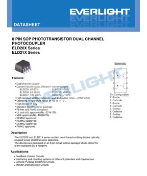
4.1 Pin Configuration and Polarity
The 8-pin SOP package has the following pinout (viewed from the top):
- Anode (Channel 1 LED)
- Cathode (Channel 1 LED)
- Anode (Channel 2 LED)
- Cathode (Channel 2 LED)
- Emitter (Channel 1 Phototransistor)
- Collector (Channel 1 Phototransistor)
- Emitter (Channel 2 Phototransistor)
- Collector (Channel 2 Phototransistor)
This symmetrical layout simplifies PCB routing for dual-channel designs.
4.2 Package Dimensions and Recommended Pad Layout
The package has a body size of approximately 4.9mm x 6.0mm with a height of 1.75mm. The datasheet includes a detailed dimensional drawing and a recommended pad layout for surface mount assembly. Following this land pattern is crucial for reliable soldering, preventing tombstoning, and ensuring proper mechanical stability. The design typically includes thermal reliefs and appropriate pad sizes to match the SOP-8 footprint.
4.3 Device Marking
Devices are marked on the top with a laser or ink code: "EL" prefix, followed by the part number (e.g., D217), a one-digit year code, a two-digit week code, and an optional "V" suffix for VDE-approved versions. This allows for traceability of manufacturing date and variant.
5. Soldering and Assembly Guidelines
The device is rated for soldering at 260°C for 10 seconds. Standard reflow profiles for lead-free (Pb-free) components should be followed. It is critical to avoid excessive thermal stress or multiple reflow cycles to prevent damage to the internal die and the plastic package. The moisture sensitivity level (MSL) should be confirmed from the full datasheet or packaging, and if required, devices should be baked before use if the packaging has been exposed to ambient humidity beyond its rated duration.
6. Packaging and Ordering Information
6.1 Model Numbering Rule
The part number follows the format: ELD2XX(Y)-V
- XX: Part number (05, 06, 07, 11, 13, 17) corresponding to the CTR grade.
- Y: Tape and reel option (TA, TB, or none). TA and TB likely differ in tape orientation or packaging specifics.
- -V: Optional suffix denoting VDE safety approval.
6.2 Packaging Specifications
The device is available in two main packaging forms:
- Tube: 100 units per tube.
- Tape and Reel: 2000 units per reel. The datasheet provides detailed tape dimensions (carrier tape width, pocket size, pitch) for both TA and TB options, which is essential for automated pick-and-place machine setup.
7. Application Suggestions
7.1 Typical Application Circuits
- Feedback Control in Switched-Mode Power Supplies (SMPS): Isolating the feedback signal from the secondary side to the primary side controller. The high CTR and speed are beneficial.
- Digital Logic Level Shifting and Interfacing: Connecting microcontrollers or logic circuits operating at different voltage levels or ground references.
- Input/Output (I/O) Isolation in PLCs and Industrial Controls: Protecting sensitive logic circuits from noisy or high-voltage field signals.
- General Purpose Switching: Driving relays, triacs, or other loads where electrical isolation is required between the control signal and the load.
7.2 Design Considerations and Notes
- LED Current Limiting: An external resistor must be used in series with the input LED to set the forward current (
IF). The value is calculated based on the supply voltage, LED forward voltage (VF), and desiredIF. The CTR is specified at specificIFpoints (1mA, 10mA). - Output Biasing: The phototransistor typically requires a pull-up resistor at the collector to VCC (output side supply). The value of this load resistor (
RL) affects both the output voltage swing and the switching speed (higher RL slows down the device). - CTR Degradation: Over very long operational lifetimes and under high temperature/current stress, the CTR of optocouplers can gradually decrease. Designs should incorporate a safety margin, especially for critical feedback loops.
- Noise Immunity: The low
CIOprovides good immunity to fast common-mode transients. For maximum noise rejection in harsh environments, keep the isolation gap on the PCB clear of copper and contaminants.
8. Technical Comparison and Differentiation
The key differentiating factors of the ELD20X/21X series compared to generic single-channel optocouplers are:
- Dual Independent Channels: Saves board space and cost compared to using two single-channel devices.
- High and Graded CTR: Offers multiple, specified gain bins for design precision, unlike parts with very wide CTR ranges.
- High Isolation Voltage (3750Vrms): Exceeds the typical 2500Vrms or 5000Vrms found in many standard optocouplers, suitable for more demanding isolation requirements.
- Wide Temperature Range: Operation from -55°C to +110°C is broader than the common commercial range (0°C to 70°C), enabling industrial and automotive use.
- Comprehensive Safety Approvals: UL, cUL, VDE, SEMKO, NEMKO, DEMKO, FIMKO approvals facilitate use in end products requiring global safety certifications.
9. Frequently Asked Questions (Based on Technical Parameters)
Q1: What is the main difference between ELD20X (e.g., ELD205) and ELD21X (e.g., ELD213) series?
A: The primary difference is in how the CTR is specified. The ELD20X series (05,06,07) provides a minimum and maximum CTR range (e.g., 40-80%), offering tighter control. The ELD21X series (11,13,17) typically specifies only a minimum CTR (e.g., >100%), which may have a wider possible upper limit.
Q2: Can I use this optocoupler for analog signal transmission?
A: While possible, phototransistor optocouplers are non-linear and their CTR varies with temperature and current. They are best suited for digital switching or "on/off" feedback signals. For linear analog isolation, a dedicated linear optocoupler or an isolation amplifier is recommended.
Q3: How do I choose the right CTR grade for my application?
A: For digital signals, choose a grade that provides sufficient output current to drive your load (e.g., pull-up resistor, logic gate input) at your chosen LED drive current, with some margin. For feedback loops where gain stability is important, a narrower range grade (like ELD205) is preferable. Lower gain parts (like ELD211) can be useful where high input current is available and output current needs to be limited.
Q4: What is the purpose of the "-V" suffix in the part number?
A: The "-V" suffix indicates that the specific unit has been tested and certified to meet VDE (German Association for Electrical, Electronic & Information Technologies) safety standards. This is often required for products sold in the European market.
10. Practical Design and Usage Case
Case: Isolated GPIO Expander for Microcontroller.
A system requires a microcontroller (3.3V logic) to monitor two digital status signals from a 24V industrial sensor module. The grounds of the two systems must be isolated. Two channels of an ELD206 optocoupler can be used. The sensor's open-collector output pulls the LED cathode (via a current-limiting resistor) to the 24V ground when active. The LED anode is connected to a 3.3V supply on the microcontroller side through a resistor. On the output, the phototransistor's collector is pulled up to the microcontroller's 3.3V supply. When the sensor is active, the LED turns on, the phototransistor saturates, pulling the collector (connected to a microcontroller GPIO pin configured as input with pull-up) low. The 3750V isolation protects the microcontroller from any faults on the 24V side. The dual channel in one package simplifies layout.
11. Operating Principle
An optocoupler's operation is based on light transmission. An electrical current applied to the input side causes an infrared Light Emitting Diode (LED) to emit photons. These photons travel across a transparent isolation gap within the package and strike the base region of a silicon phototransistor on the output side. This light energy generates electron-hole pairs in the base, effectively acting as a base current and turning the transistor on, allowing a proportional collector current to flow. The key point is that the signal is transferred by light, not by an electrical connection, thereby achieving galvanic isolation determined by the physical and dielectric properties of the isolation gap.
12. Technology Trends
The trend in optocoupler technology is towards higher speed, lower power consumption, and greater integration. While traditional phototransistor couplers like this one are workhorses for medium-speed digital isolation, newer technologies are emerging:
- Digital Isolators: Use CMOS chips and RF or capacitive coupling to achieve much higher data rates (>>1 Mbps), lower power, and longer lifetime, but may have different isolation material characteristics.
- Higher Integration: Combining multiple isolation channels with other functions like gate drivers or ADC/DAC converters.
- Improved Robustness: Ongoing development of packaging and materials to enhance reliability, thermal performance, and immunity to harsh environmental factors like humidity.
Phototransistor optocouplers remain highly relevant due to their simplicity, cost-effectiveness, high voltage capability, and well-understood characteristics, especially in power electronics and industrial control applications where very high speeds are not the primary requirement.
LED Specification Terminology
Complete explanation of LED technical terms
Photoelectric Performance
| Term | Unit/Representation | Simple Explanation | Why Important |
|---|---|---|---|
| Luminous Efficacy | lm/W (lumens per watt) | Light output per watt of electricity, higher means more energy efficient. | Directly determines energy efficiency grade and electricity cost. |
| Luminous Flux | lm (lumens) | Total light emitted by source, commonly called "brightness". | Determines if the light is bright enough. |
| Viewing Angle | ° (degrees), e.g., 120° | Angle where light intensity drops to half, determines beam width. | Affects illumination range and uniformity. |
| CCT (Color Temperature) | K (Kelvin), e.g., 2700K/6500K | Warmth/coolness of light, lower values yellowish/warm, higher whitish/cool. | Determines lighting atmosphere and suitable scenarios. |
| CRI / Ra | Unitless, 0–100 | Ability to render object colors accurately, Ra≥80 is good. | Affects color authenticity, used in high-demand places like malls, museums. |
| SDCM | MacAdam ellipse steps, e.g., "5-step" | Color consistency metric, smaller steps mean more consistent color. | Ensures uniform color across same batch of LEDs. |
| Dominant Wavelength | nm (nanometers), e.g., 620nm (red) | Wavelength corresponding to color of colored LEDs. | Determines hue of red, yellow, green monochrome LEDs. |
| Spectral Distribution | Wavelength vs intensity curve | Shows intensity distribution across wavelengths. | Affects color rendering and quality. |
Electrical Parameters
| Term | Symbol | Simple Explanation | Design Considerations |
|---|---|---|---|
| Forward Voltage | Vf | Minimum voltage to turn on LED, like "starting threshold". | Driver voltage must be ≥Vf, voltages add up for series LEDs. |
| Forward Current | If | Current value for normal LED operation. | Usually constant current drive, current determines brightness & lifespan. |
| Max Pulse Current | Ifp | Peak current tolerable for short periods, used for dimming or flashing. | Pulse width & duty cycle must be strictly controlled to avoid damage. |
| Reverse Voltage | Vr | Max reverse voltage LED can withstand, beyond may cause breakdown. | Circuit must prevent reverse connection or voltage spikes. |
| Thermal Resistance | Rth (°C/W) | Resistance to heat transfer from chip to solder, lower is better. | High thermal resistance requires stronger heat dissipation. |
| ESD Immunity | V (HBM), e.g., 1000V | Ability to withstand electrostatic discharge, higher means less vulnerable. | Anti-static measures needed in production, especially for sensitive LEDs. |
Thermal Management & Reliability
| Term | Key Metric | Simple Explanation | Impact |
|---|---|---|---|
| Junction Temperature | Tj (°C) | Actual operating temperature inside LED chip. | Every 10°C reduction may double lifespan; too high causes light decay, color shift. |
| Lumen Depreciation | L70 / L80 (hours) | Time for brightness to drop to 70% or 80% of initial. | Directly defines LED "service life". |
| Lumen Maintenance | % (e.g., 70%) | Percentage of brightness retained after time. | Indicates brightness retention over long-term use. |
| Color Shift | Δu′v′ or MacAdam ellipse | Degree of color change during use. | Affects color consistency in lighting scenes. |
| Thermal Aging | Material degradation | Deterioration due to long-term high temperature. | May cause brightness drop, color change, or open-circuit failure. |
Packaging & Materials
| Term | Common Types | Simple Explanation | Features & Applications |
|---|---|---|---|
| Package Type | EMC, PPA, Ceramic | Housing material protecting chip, providing optical/thermal interface. | EMC: good heat resistance, low cost; Ceramic: better heat dissipation, longer life. |
| Chip Structure | Front, Flip Chip | Chip electrode arrangement. | Flip chip: better heat dissipation, higher efficacy, for high-power. |
| Phosphor Coating | YAG, Silicate, Nitride | Covers blue chip, converts some to yellow/red, mixes to white. | Different phosphors affect efficacy, CCT, and CRI. |
| Lens/Optics | Flat, Microlens, TIR | Optical structure on surface controlling light distribution. | Determines viewing angle and light distribution curve. |
Quality Control & Binning
| Term | Binning Content | Simple Explanation | Purpose |
|---|---|---|---|
| Luminous Flux Bin | Code e.g., 2G, 2H | Grouped by brightness, each group has min/max lumen values. | Ensures uniform brightness in same batch. |
| Voltage Bin | Code e.g., 6W, 6X | Grouped by forward voltage range. | Facilitates driver matching, improves system efficiency. |
| Color Bin | 5-step MacAdam ellipse | Grouped by color coordinates, ensuring tight range. | Guarantees color consistency, avoids uneven color within fixture. |
| CCT Bin | 2700K, 3000K etc. | Grouped by CCT, each has corresponding coordinate range. | Meets different scene CCT requirements. |
Testing & Certification
| Term | Standard/Test | Simple Explanation | Significance |
|---|---|---|---|
| LM-80 | Lumen maintenance test | Long-term lighting at constant temperature, recording brightness decay. | Used to estimate LED life (with TM-21). |
| TM-21 | Life estimation standard | Estimates life under actual conditions based on LM-80 data. | Provides scientific life prediction. |
| IESNA | Illuminating Engineering Society | Covers optical, electrical, thermal test methods. | Industry-recognized test basis. |
| RoHS / REACH | Environmental certification | Ensures no harmful substances (lead, mercury). | Market access requirement internationally. |
| ENERGY STAR / DLC | Energy efficiency certification | Energy efficiency and performance certification for lighting. | Used in government procurement, subsidy programs, enhances competitiveness. |