Table of Contents
- 1. Product Overview
- 1.1 Core Advantages and Target Market
- 2. In-Depth Technical Parameter Analysis
- 2.1 Absolute Maximum Ratings
- 2.2 Recommended Operating Conditions
- 2.3 Electro-Optical Characteristics
- 3. Performance Curve Analysis
- 3.1 Power Supply Voltage vs. Minimum Receiver Power
- 3.2 Transfer Rate vs. Minimum Receiver Power
- 4. Mechanical and Package Information
- 4.1 Package Dimension and Pinout
- 5. Application and Design Guidelines
- 5.1 Typical Application Circuit
- 5.2 Measuring Methods
- 6. Packaging and Ordering Information
- 6.1 Label Explanation and Packing
- 7. Compliance and Reliability Notes
- 8. Design Considerations and FAQs
- 8.1 Key Design Considerations
- 8.2 Frequently Asked Questions (Based on Technical Parameters)
- 9. Principle of Operation
- 10. Application Scenarios and Use Cases
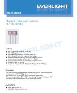
1. Product Overview
The PLR137 series represents a high-performance fiber optic receiver module designed for digital optical data transmission. It is engineered to convert optical signals into electrical TTL-compatible outputs, facilitating reliable data communication over plastic optical fiber (POF) cables. The core of the device is a proprietary CMOS Photodetector Integrated Circuit (PDIC), which enables high sensitivity and low power consumption. This product is optimized for use with red light sources, typically around 650nm wavelength, making it suitable for a range of consumer and industrial digital interface applications where noise immunity and extended battery life are critical.
1.1 Core Advantages and Target Market
The PLR137 series offers several key advantages that position it favorably in the market. Its high photodetector sensitivity, optimized for red light, allows for longer transmission distances or the use of lower-power transmitters. The built-in threshold control circuit significantly improves the noise margin, enhancing signal integrity in electrically noisy environments. Furthermore, its low power consumption is a decisive factor for portable and battery-operated devices. The primary target markets include digital audio interfaces (such as Dolby AC-3), industrial data links, and any application requiring a robust, short-to-medium range optical communication link that is immune to electromagnetic interference.
2. In-Depth Technical Parameter Analysis
This section provides a detailed, objective interpretation of the key technical parameters specified in the datasheet. Understanding these parameters is crucial for proper circuit design and system integration.
2.1 Absolute Maximum Ratings
The absolute maximum ratings define the stress limits beyond which permanent damage to the device may occur. The supply voltage (Vcc) must never exceed 5.5V or go below -0.5V. The output pin voltage should not be forced above Vcc + 0.3V. The device can be stored in temperatures from -40°C to 85°C but operates within a narrower range of -20°C to 70°C. A critical parameter for assembly is the soldering temperature, rated at 260°C for a maximum duration of 10 seconds, which is typical for lead-free reflow processes. Electrostatic discharge (ESD) protection is 2000V (Human Body Model) and 100V (Machine Model), indicating standard handling precautions are necessary.
2.2 Recommended Operating Conditions
For reliable operation, the device should be powered within the recommended supply voltage range of 2.4V to 5.5V, with a typical value of 3.0V. Operating outside this range may lead to degraded performance or failure to meet other specified characteristics.
2.3 Electro-Optical Characteristics
These parameters, measured at 25°C, Vcc=3V, and a load capacitance of 5pF, define the receiver's performance.
- Peak Sensitivity Wavelength (λp): 650 nm. The receiver is most sensitive to red light at this wavelength.
- Transmission Distance (d): 0.2 to 5 meters. This range is typical for standard plastic optical fiber.
- Receiver Power (Pc): The minimum required optical power (sensitivity) is -27 dBm (minimum) at 16 Mbps. The maximum allowable input power before potential damage or distortion is -14 dBm. The difference between these values is the dynamic range.
- Dissipation Current (Icc): Typically 4 mA, with a maximum of 12 mA. This low current is key for battery life.
- Output Voltage Levels: The TTL-compatible output provides a high level (VOH) of typically 2.5V (min 2.1V) and a low level (VOL) of typically 0.2V (max 0.4V).
- Timing Parameters: Rise and fall times (tr, tf) are typically 10 ns (max 20 ns). Propagation delays (tPLH, tPHL) are up to 120 ns. Pulse width distortion (Δtw) is within ±25 ns, and jitter (Δtj) ranges from 1-20 ns depending on input power.
- Transfer Rate (T): Supports Non-Return-to-Zero (NRZ) signals from 0.1 Mbps up to 16 Mbps.
3. Performance Curve Analysis
The datasheet includes typical performance curves that provide insight into behavior under varying conditions.
3.1 Power Supply Voltage vs. Minimum Receiver Power
Figure 4 illustrates how the minimum receiver power (sensitivity) changes with the operating voltage. Generally, sensitivity may improve slightly at higher voltages within the operating range. This curve is essential for designers to confirm adequate link margin when operating at voltages other than the typical 3.3V.
3.2 Transfer Rate vs. Minimum Receiver Power
Figure 5 shows the relationship between data rate and required optical input power. As the data rate increases, the receiver typically requires more optical power (less negative dBm) to maintain a low bit error rate. This curve is critical for determining the maximum achievable distance at a desired data rate or for selecting an appropriate transmitter power.
4. Mechanical and Package Information
4.1 Package Dimension and Pinout
The device comes in a standard 3-pin package. The pin functions are: Pin 1: Vout (Output), Pin 2: GND (Ground), Pin 3: Vcc (Supply Voltage). The critical mechanical dimension is the pin length (A1), which varies by device variant (e.g., PLR137, PLR137/S, PLR137/S9, etc.), ranging from 8.00 mm to 16.00 mm. All dimensions have a general tolerance of ±0.10 mm. The specific variant must be selected based on the mechanical requirements of the host connector or PCB mounting.
5. Application and Design Guidelines
5.1 Typical Application Circuit
The datasheet provides two general application circuits for 3V and 5V operation. Both circuits require external decoupling and filtering components. A 0.1µF capacitor (C1) must be placed close to the Vcc and GND pins (within 7mm for good coupling) to decouple high-frequency noise. An optional 30pF capacitor (C2) across the output can help reduce ringing. A 47µH inductor (L2) in series with the power supply may be used for additional noise filtering. The choice between the 3V and 5V circuit depends on the available system voltage and the desired output swing.
5.2 Measuring Methods
The document outlines standard methods for characterizing the device. Figure 1 details how to measure maximum and minimum input power using a control circuit, transmitter, standard POF cable, and an optical power meter. Figure 2 shows the setup for measuring supply current. Figure 3 illustrates the test circuit and definitions for output voltage, pulse timing parameters (rise/fall time, propagation delay), and jitter.
6. Packaging and Ordering Information
6.1 Label Explanation and Packing
The product label contains several codes: CPN (Customer's Product Number), P/N (Product Number), QTY (Packing Quantity), LOT No (Lot Number), and reference codes for various ranks (not typically used for this digital receiver). The standard packing options are 500 pieces per bag or 2000 pieces per bag, with 4 bags per box.
7. Compliance and Reliability Notes
The product is designed to comply with key environmental regulations. It is stated to remain within RoHS (Restriction of Hazardous Substances) compliant versions, complies with EU REACH regulations, and is Halogen-Free (Bromine <900ppm, Chlorine <900ppm, Br+Cl <1500ppm). These compliances are important for meeting global environmental standards in electronic products.
8. Design Considerations and FAQs
8.1 Key Design Considerations
- Link Budget: Always calculate the link budget by comparing your transmitter's output power (coupled into the fiber) with the receiver's sensitivity at your operating data rate and voltage. Include connector losses and margin for aging.
- Power Supply Decoupling: The 0.1µF capacitor must be placed as close as possible to the receiver pins to ensure stable operation and minimize noise.
- Fiber Alignment: Proper mechanical alignment between the fiber and the receiver's photodetector is critical for maximizing coupled optical power.
- Signal Integrity: For high-speed operation near 16 Mbps, consider the effects of jitter and pulse width distortion on your system's timing margins.
8.2 Frequently Asked Questions (Based on Technical Parameters)
Q: Can I use this receiver with an 850nm infrared light source?
A: No. The receiver is optimized for a peak sensitivity wavelength of 650nm (red light). Its sensitivity will be significantly lower at 850nm, potentially rendering the link non-functional.
Q: What is the maximum data rate supported?
A: The guaranteed maximum data rate for NRZ signaling is 16 Mbps under the specified conditions. Operation beyond this rate is not characterized.
Q: How do I select the correct device variant (e.g., PLR137/S vs. PLR137/S9)?
A: The selection is based solely on the required pin length (A1 dimension) for your specific mechanical housing or connector. Refer to the Device Selection Table in the Package Dimension section.
Q: Is an external amplifier needed?
A: No. The device integrates a sensitive photodetector and a threshold-controlled amplifier on a single CMOS PDIC, providing a direct TTL-level output.
9. Principle of Operation
The PLR137 operates on the principle of internal photoelectric effect. Incoming photons of light, typically at 650nm, strike the integrated photodetector within the CMOS PDIC. This generates electron-hole pairs, resulting in a small photocurrent proportional to the optical power. This current is then amplified and processed by the integrated circuitry. A key feature is the built-in threshold control circuit, which sets a decision level to distinguish between logical '0' and '1' states, improving immunity to noise and variations in average optical power. The final output is a regenerated, TTL-compatible digital signal.
10. Application Scenarios and Use Cases
Digital Audio Interface: A primary application is in Dolby AC-3 digital audio interfaces, where it provides an electrically isolated, high-fidelity link between components like DVD players and audio receivers, eliminating ground loops and hum.
Industrial Data-Link: In factory automation, the receiver can be used in sensor networks or control links where high levels of electromagnetic interference (EMI) from motors and drives would corrupt electrical cables.
Medical Equipment: For non-critical data monitoring within medical devices, the optical isolation can enhance patient safety by breaking galvanic connections.
Consumer Electronics: Potential use in high-end gaming consoles or VR systems for low-latency, interference-free data transfer between modules.
LED Specification Terminology
Complete explanation of LED technical terms
Photoelectric Performance
| Term | Unit/Representation | Simple Explanation | Why Important |
|---|---|---|---|
| Luminous Efficacy | lm/W (lumens per watt) | Light output per watt of electricity, higher means more energy efficient. | Directly determines energy efficiency grade and electricity cost. |
| Luminous Flux | lm (lumens) | Total light emitted by source, commonly called "brightness". | Determines if the light is bright enough. |
| Viewing Angle | ° (degrees), e.g., 120° | Angle where light intensity drops to half, determines beam width. | Affects illumination range and uniformity. |
| CCT (Color Temperature) | K (Kelvin), e.g., 2700K/6500K | Warmth/coolness of light, lower values yellowish/warm, higher whitish/cool. | Determines lighting atmosphere and suitable scenarios. |
| CRI / Ra | Unitless, 0–100 | Ability to render object colors accurately, Ra≥80 is good. | Affects color authenticity, used in high-demand places like malls, museums. |
| SDCM | MacAdam ellipse steps, e.g., "5-step" | Color consistency metric, smaller steps mean more consistent color. | Ensures uniform color across same batch of LEDs. |
| Dominant Wavelength | nm (nanometers), e.g., 620nm (red) | Wavelength corresponding to color of colored LEDs. | Determines hue of red, yellow, green monochrome LEDs. |
| Spectral Distribution | Wavelength vs intensity curve | Shows intensity distribution across wavelengths. | Affects color rendering and quality. |
Electrical Parameters
| Term | Symbol | Simple Explanation | Design Considerations |
|---|---|---|---|
| Forward Voltage | Vf | Minimum voltage to turn on LED, like "starting threshold". | Driver voltage must be ≥Vf, voltages add up for series LEDs. |
| Forward Current | If | Current value for normal LED operation. | Usually constant current drive, current determines brightness & lifespan. |
| Max Pulse Current | Ifp | Peak current tolerable for short periods, used for dimming or flashing. | Pulse width & duty cycle must be strictly controlled to avoid damage. |
| Reverse Voltage | Vr | Max reverse voltage LED can withstand, beyond may cause breakdown. | Circuit must prevent reverse connection or voltage spikes. |
| Thermal Resistance | Rth (°C/W) | Resistance to heat transfer from chip to solder, lower is better. | High thermal resistance requires stronger heat dissipation. |
| ESD Immunity | V (HBM), e.g., 1000V | Ability to withstand electrostatic discharge, higher means less vulnerable. | Anti-static measures needed in production, especially for sensitive LEDs. |
Thermal Management & Reliability
| Term | Key Metric | Simple Explanation | Impact |
|---|---|---|---|
| Junction Temperature | Tj (°C) | Actual operating temperature inside LED chip. | Every 10°C reduction may double lifespan; too high causes light decay, color shift. |
| Lumen Depreciation | L70 / L80 (hours) | Time for brightness to drop to 70% or 80% of initial. | Directly defines LED "service life". |
| Lumen Maintenance | % (e.g., 70%) | Percentage of brightness retained after time. | Indicates brightness retention over long-term use. |
| Color Shift | Δu′v′ or MacAdam ellipse | Degree of color change during use. | Affects color consistency in lighting scenes. |
| Thermal Aging | Material degradation | Deterioration due to long-term high temperature. | May cause brightness drop, color change, or open-circuit failure. |
Packaging & Materials
| Term | Common Types | Simple Explanation | Features & Applications |
|---|---|---|---|
| Package Type | EMC, PPA, Ceramic | Housing material protecting chip, providing optical/thermal interface. | EMC: good heat resistance, low cost; Ceramic: better heat dissipation, longer life. |
| Chip Structure | Front, Flip Chip | Chip electrode arrangement. | Flip chip: better heat dissipation, higher efficacy, for high-power. |
| Phosphor Coating | YAG, Silicate, Nitride | Covers blue chip, converts some to yellow/red, mixes to white. | Different phosphors affect efficacy, CCT, and CRI. |
| Lens/Optics | Flat, Microlens, TIR | Optical structure on surface controlling light distribution. | Determines viewing angle and light distribution curve. |
Quality Control & Binning
| Term | Binning Content | Simple Explanation | Purpose |
|---|---|---|---|
| Luminous Flux Bin | Code e.g., 2G, 2H | Grouped by brightness, each group has min/max lumen values. | Ensures uniform brightness in same batch. |
| Voltage Bin | Code e.g., 6W, 6X | Grouped by forward voltage range. | Facilitates driver matching, improves system efficiency. |
| Color Bin | 5-step MacAdam ellipse | Grouped by color coordinates, ensuring tight range. | Guarantees color consistency, avoids uneven color within fixture. |
| CCT Bin | 2700K, 3000K etc. | Grouped by CCT, each has corresponding coordinate range. | Meets different scene CCT requirements. |
Testing & Certification
| Term | Standard/Test | Simple Explanation | Significance |
|---|---|---|---|
| LM-80 | Lumen maintenance test | Long-term lighting at constant temperature, recording brightness decay. | Used to estimate LED life (with TM-21). |
| TM-21 | Life estimation standard | Estimates life under actual conditions based on LM-80 data. | Provides scientific life prediction. |
| IESNA | Illuminating Engineering Society | Covers optical, electrical, thermal test methods. | Industry-recognized test basis. |
| RoHS / REACH | Environmental certification | Ensures no harmful substances (lead, mercury). | Market access requirement internationally. |
| ENERGY STAR / DLC | Energy efficiency certification | Energy efficiency and performance certification for lighting. | Used in government procurement, subsidy programs, enhances competitiveness. |