Table of Contents
- 1. Product Overview
- 1.1 Core Features and Positioning
- 1.2 Compliance and Environmental Specifications
- 2. Technical Parameter Analysis
- 2.1 Absolute Maximum Ratings
- 2.2 Electro-Optical Characteristics
- 3. Performance Curve Analysis
- 3.1 Forward Current vs. Ambient Temperature
- 3.2 Spectral Distribution
- 3.3 Relative Intensity vs. Forward Current
- 3.4 Forward Current vs. Forward Voltage
- 3.5 Relative Radiant Intensity vs. Angular Displacement
- 4. Mechanical and Packaging Information
- 4.1 Package Dimensions
- 4.2 Polarity Identification
- 4.3 Packaging for Assembly
- 5. Soldering and Assembly Guidelines
- 5.1 Storage and Moisture Sensitivity
- 5.2 Reflow Soldering Profile
- 5.3 Hand Soldering and Rework
- 6. Application Notes and Design Considerations
- 6.1 Primary Application Scenarios
- 6.2 Critical Design Considerations
- 6.3 Comparison and Selection Factors
- 7. Labeling and Ordering Information
- 8. Technical Principles and Trends
- 8.1 Operating Principle
- 8.2 Industry Trends
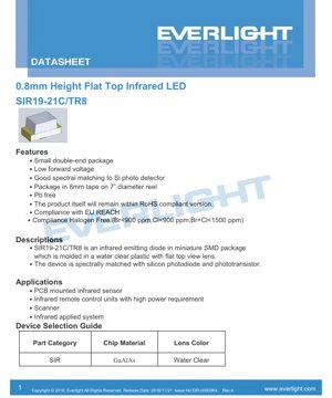
1. Product Overview
This document provides the complete technical specifications for a miniature, surface-mount infrared (IR) emitting diode. The device is designed for applications requiring a compact, reliable source of infrared light matched to silicon photodetectors.
1.1 Core Features and Positioning
The LED is characterized by its exceptionally low profile of 0.8mm, making it suitable for space-constrained PCB designs. It features a flat-top lens molded from clear plastic, which provides a specific radiation pattern. The device is constructed using a GaAlAs (Gallium Aluminum Arsenide) chip material, which is optimized for infrared emission. A key design advantage is its spectral output, which is closely matched to the sensitivity curve of common silicon photodiodes and phototransistors, maximizing detection efficiency in sensor systems.
1.2 Compliance and Environmental Specifications
The component is compliant with major environmental and safety directives. It is manufactured as a Pb-free (lead-free) product. It also complies with halogen-free requirements, specifically limiting Bromine (Br) and Chlorine (Cl) content to less than 900 ppm individually and a combined total of less than 1500 ppm. The product is designed to remain within the parameters of the RoHS (Restriction of Hazardous Substances) directive.
2. Technical Parameter Analysis
This section details the absolute limits and standard operating characteristics of the infrared LED. All parameters are specified at an ambient temperature (Ta) of 25°C unless otherwise noted.
2.1 Absolute Maximum Ratings
These ratings define the stress limits beyond which permanent damage to the device may occur. Operation under or at these limits is not guaranteed.
- Continuous Forward Current (IF): 65 mA
- Reverse Voltage (VR): 5 V
- Operating Temperature (Topr): -25°C to +85°C
- Storage Temperature (Tstg): -40°C to +85°C
- Soldering Temperature (Tsol): 260°C for a duration not exceeding 5 seconds.
- Power Dissipation (Pd): 110 mW (at or below 25°C free air temperature).
2.2 Electro-Optical Characteristics
These parameters define the typical performance of the device under standard test conditions (IF = 20mA, Ta=25°C).
- Radiant Intensity (Ie): 0.2 mW/sr (Minimum), 0.5 mW/sr (Typical). This measures the optical power emitted per unit solid angle.
- Peak Wavelength (λp): 875 nm (Typical). This is the wavelength at which the optical output is strongest.
- Spectral Bandwidth (Δλ): 80 nm (Typical). This indicates the range of wavelengths emitted, typically measured at half the peak intensity (FWHM).
- Forward Voltage (VF): 1.3 V (Typical), 1.6 V (Maximum). The voltage drop across the LED when conducting 20mA.
- Reverse Current (IR): 10 µA (Maximum). The leakage current when 5V is applied in reverse bias.
- View Angle (2θ1/2): 145° (Typical). The full angle at which the radiant intensity is half of the peak intensity (at 0°). The flat-top lens contributes to this wide viewing angle.
3. Performance Curve Analysis
The datasheet includes several graphs illustrating the device's behavior under varying conditions. These curves are essential for design engineers to predict performance in real-world applications.
3.1 Forward Current vs. Ambient Temperature
This curve shows the derating of the maximum allowable forward current as the ambient temperature increases. To prevent thermal damage, the forward current must be reduced when operating above 25°C. The power dissipation rating of 110mW is a critical factor in this derating calculation.
3.2 Spectral Distribution
The graph depicts the relative optical power output across the wavelength spectrum. It confirms the peak emission at approximately 875nm and the ~80nm spectral bandwidth, highlighting the match with silicon detector sensitivity (which peaks around 800-900nm).
3.3 Relative Intensity vs. Forward Current
This plot illustrates the relationship between the drive current and the light output. It typically shows a sub-linear trend, where increasing the current yields diminishing returns in radiant intensity, especially as thermal effects become significant. This informs decisions on drive current for desired output versus efficiency and device lifetime.
3.4 Forward Current vs. Forward Voltage
The IV (Current-Voltage) curve is fundamental for circuit design. It shows the exponential relationship, allowing designers to calculate the necessary series resistor for a given supply voltage to achieve the target drive current (e.g., 20mA). The typical VF of 1.3V is a key value for these calculations.
3.5 Relative Radiant Intensity vs. Angular Displacement
This polar plot visually represents the radiation pattern or view angle. The 145° viewing angle is confirmed here, showing how intensity decreases as the angle from the central axis (0°) increases. This is crucial for aligning the LED with a detector in sensor applications.
4. Mechanical and Packaging Information
4.1 Package Dimensions
The device is housed in a very compact surface-mount package. Key dimensions include a body size of approximately 1.6mm x 1.2mm with a total height of 0.8mm. The anode and cathode pads are located on the bottom of the package. Detailed mechanical drawings in the datasheet provide all critical dimensions with a standard tolerance of ±0.1mm unless otherwise specified. A suggested land pattern (footprint) for PCB design is provided as a reference, but designers are advised to modify it based on their specific assembly process and reliability requirements.
4.2 Polarity Identification
The package includes a polarity indicator, typically a notch or a mark on one end, to distinguish the anode from the cathode. Correct orientation is vital for circuit operation.
4.3 Packaging for Assembly
The components are supplied on tape and reel for compatibility with automated pick-and-place assembly equipment. The tape width is 8mm, wound on a standard 7-inch diameter reel. Each reel contains 3000 pieces. Carrier tape dimensions are provided to ensure compatibility with feeder systems.
5. Soldering and Assembly Guidelines
Proper handling is critical to maintain device reliability and performance.
5.1 Storage and Moisture Sensitivity
The LEDs are packaged in a moisture-proof bag with desiccant. The bag should not be opened until the components are ready for use. Before opening, store at 10-30°C with ≤90% RH. After opening, the "floor life" is 168 hours (7 days) when stored at 10-30°C and ≤60% RH. Unused parts must be re-bagged with desiccant. If the floor life or shelf life is exceeded, baking at 60°C ±5°C for 96 hours is required before use to remove absorbed moisture and prevent "popcorning" during reflow soldering.
5.2 Reflow Soldering Profile
A recommended Pb-free reflow soldering temperature profile is provided. Key parameters include a preheat stage, a defined ramp-up rate, a peak temperature not exceeding 260°C, and a time above liquidus (TAL) appropriate for the solder paste. Reflow soldering should not be performed more than two times on the same device. Stress on the LED body during heating and warping of the PCB after soldering must be avoided.
5.3 Hand Soldering and Rework
If hand soldering is necessary, extreme care is required. The soldering iron tip temperature should be below 350°C, applied to each terminal for no more than 3 seconds. A low-power iron (≤25W) is recommended. A cooling interval of at least 2 seconds should be allowed between soldering the two terminals. Rework is strongly discouraged after the LED is soldered. If unavoidable, a specialized dual-tip soldering iron must be used to simultaneously heat both terminals and lift the component without applying mechanical stress. The impact of rework on device characteristics must be verified beforehand.
6. Application Notes and Design Considerations
6.1 Primary Application Scenarios
- PCB-Mounted Infrared Sensors: Proximity sensing, object detection, line following.
- Infrared Remote Control Units: Suitable for designs requiring higher output power for extended range.
- Scanners: Barcode readers, document scanners.
- General Infrared Systems: Any application requiring a compact, efficient IR source paired with a silicon detector.
6.2 Critical Design Considerations
- Current Limiting: An external series resistor is MANDATORY. The LED's exponential IV characteristic means a small increase in voltage can cause a large, destructive increase in current. The resistor value is calculated using R = (Vsupply - VF) / IF.
- Thermal Management: The 110mW power dissipation limit must be respected. Consider PCB copper area (thermal pads) for heat sinking, especially when driving at higher currents or in elevated ambient temperatures.
- Optical Alignment: The wide 145° viewing angle simplifies alignment but reduces intensity at a specific point. For focused beams, external optics may be required.
- Electrical Protection: The low reverse voltage rating (5V) means care must be taken to avoid reverse bias conditions, which could be caused by inductive loads or incorrect PCB layout.
6.3 Comparison and Selection Factors
When selecting an IR LED, key differentiating factors include:
Package Size/Height: This device's 0.8mm profile is a major advantage for ultra-thin designs.
Viewing Angle: The flat-top, wide-angle lens is ideal for broad coverage, whereas domed lenses offer more focused beams.
Wavelength: The 875nm peak is a standard matched to silicon. Other wavelengths (e.g., 940nm) offer lower visibility but may have slightly lower detector response.
Radiant Intensity: The 0.5mW/sr typical output is suitable for many medium-range applications. Higher-output devices are available but may trade off size or viewing angle.
7. Labeling and Ordering Information
The reel label contains essential information for traceability and production control. Fields typically include: Customer Part Number (CPN), Manufacturer Part Number (P/N), Lot Number (LOT No), Quantity (QTY), Peak Wavelength (H.E.), Performance Rank (CAT), Reference Code (REF), Moisture Sensitivity Level (MSL-X), and Country of Manufacture (Made In). The specific part number for this device is SIR19-21C/TR8, where "TR8" indicates the 8mm tape on reel packaging.
8. Technical Principles and Trends
8.1 Operating Principle
An infrared LED is a semiconductor p-n junction diode. When forward biased, electrons and holes recombine in the active region (the GaAlAs chip), releasing energy in the form of photons. The specific bandgap energy of the GaAlAs material determines the photon wavelength, resulting in infrared light around 875nm. The clear epoxy lens protects the chip and shapes the emitted light pattern.
8.2 Industry Trends
The trend in SMD optoelectronics continues toward miniaturization, higher efficiency, and greater integration. There is increasing demand for even smaller package footprints and lower heights to enable thinner consumer electronics. Advances in chip design and packaging materials aim to deliver higher radiant intensity from smaller devices while maintaining or improving reliability. Integration with drivers and sensors in multi-chip modules (MCMs) or system-in-package (SiP) solutions is also a growing area, simplifying design and saving board space.
LED Specification Terminology
Complete explanation of LED technical terms
Photoelectric Performance
| Term | Unit/Representation | Simple Explanation | Why Important |
|---|---|---|---|
| Luminous Efficacy | lm/W (lumens per watt) | Light output per watt of electricity, higher means more energy efficient. | Directly determines energy efficiency grade and electricity cost. |
| Luminous Flux | lm (lumens) | Total light emitted by source, commonly called "brightness". | Determines if the light is bright enough. |
| Viewing Angle | ° (degrees), e.g., 120° | Angle where light intensity drops to half, determines beam width. | Affects illumination range and uniformity. |
| CCT (Color Temperature) | K (Kelvin), e.g., 2700K/6500K | Warmth/coolness of light, lower values yellowish/warm, higher whitish/cool. | Determines lighting atmosphere and suitable scenarios. |
| CRI / Ra | Unitless, 0–100 | Ability to render object colors accurately, Ra≥80 is good. | Affects color authenticity, used in high-demand places like malls, museums. |
| SDCM | MacAdam ellipse steps, e.g., "5-step" | Color consistency metric, smaller steps mean more consistent color. | Ensures uniform color across same batch of LEDs. |
| Dominant Wavelength | nm (nanometers), e.g., 620nm (red) | Wavelength corresponding to color of colored LEDs. | Determines hue of red, yellow, green monochrome LEDs. |
| Spectral Distribution | Wavelength vs intensity curve | Shows intensity distribution across wavelengths. | Affects color rendering and quality. |
Electrical Parameters
| Term | Symbol | Simple Explanation | Design Considerations |
|---|---|---|---|
| Forward Voltage | Vf | Minimum voltage to turn on LED, like "starting threshold". | Driver voltage must be ≥Vf, voltages add up for series LEDs. |
| Forward Current | If | Current value for normal LED operation. | Usually constant current drive, current determines brightness & lifespan. |
| Max Pulse Current | Ifp | Peak current tolerable for short periods, used for dimming or flashing. | Pulse width & duty cycle must be strictly controlled to avoid damage. |
| Reverse Voltage | Vr | Max reverse voltage LED can withstand, beyond may cause breakdown. | Circuit must prevent reverse connection or voltage spikes. |
| Thermal Resistance | Rth (°C/W) | Resistance to heat transfer from chip to solder, lower is better. | High thermal resistance requires stronger heat dissipation. |
| ESD Immunity | V (HBM), e.g., 1000V | Ability to withstand electrostatic discharge, higher means less vulnerable. | Anti-static measures needed in production, especially for sensitive LEDs. |
Thermal Management & Reliability
| Term | Key Metric | Simple Explanation | Impact |
|---|---|---|---|
| Junction Temperature | Tj (°C) | Actual operating temperature inside LED chip. | Every 10°C reduction may double lifespan; too high causes light decay, color shift. |
| Lumen Depreciation | L70 / L80 (hours) | Time for brightness to drop to 70% or 80% of initial. | Directly defines LED "service life". |
| Lumen Maintenance | % (e.g., 70%) | Percentage of brightness retained after time. | Indicates brightness retention over long-term use. |
| Color Shift | Δu′v′ or MacAdam ellipse | Degree of color change during use. | Affects color consistency in lighting scenes. |
| Thermal Aging | Material degradation | Deterioration due to long-term high temperature. | May cause brightness drop, color change, or open-circuit failure. |
Packaging & Materials
| Term | Common Types | Simple Explanation | Features & Applications |
|---|---|---|---|
| Package Type | EMC, PPA, Ceramic | Housing material protecting chip, providing optical/thermal interface. | EMC: good heat resistance, low cost; Ceramic: better heat dissipation, longer life. |
| Chip Structure | Front, Flip Chip | Chip electrode arrangement. | Flip chip: better heat dissipation, higher efficacy, for high-power. |
| Phosphor Coating | YAG, Silicate, Nitride | Covers blue chip, converts some to yellow/red, mixes to white. | Different phosphors affect efficacy, CCT, and CRI. |
| Lens/Optics | Flat, Microlens, TIR | Optical structure on surface controlling light distribution. | Determines viewing angle and light distribution curve. |
Quality Control & Binning
| Term | Binning Content | Simple Explanation | Purpose |
|---|---|---|---|
| Luminous Flux Bin | Code e.g., 2G, 2H | Grouped by brightness, each group has min/max lumen values. | Ensures uniform brightness in same batch. |
| Voltage Bin | Code e.g., 6W, 6X | Grouped by forward voltage range. | Facilitates driver matching, improves system efficiency. |
| Color Bin | 5-step MacAdam ellipse | Grouped by color coordinates, ensuring tight range. | Guarantees color consistency, avoids uneven color within fixture. |
| CCT Bin | 2700K, 3000K etc. | Grouped by CCT, each has corresponding coordinate range. | Meets different scene CCT requirements. |
Testing & Certification
| Term | Standard/Test | Simple Explanation | Significance |
|---|---|---|---|
| LM-80 | Lumen maintenance test | Long-term lighting at constant temperature, recording brightness decay. | Used to estimate LED life (with TM-21). |
| TM-21 | Life estimation standard | Estimates life under actual conditions based on LM-80 data. | Provides scientific life prediction. |
| IESNA | Illuminating Engineering Society | Covers optical, electrical, thermal test methods. | Industry-recognized test basis. |
| RoHS / REACH | Environmental certification | Ensures no harmful substances (lead, mercury). | Market access requirement internationally. |
| ENERGY STAR / DLC | Energy efficiency certification | Energy efficiency and performance certification for lighting. | Used in government procurement, subsidy programs, enhances competitiveness. |