Table of Contents
- 1. Product Overview
- 2. Technical Parameter Deep-Dive
- 2.1 Absolute Maximum Ratings
- 2.2 Electro-Optical Characteristics
- 3. Binning System Explanation
- 3.1 Luminous Intensity Binning
- 3.2 Forward Voltage Binning
- 3.3 Color Combination
- 4. Performance Curve Analysis
- 4.1 Relative Intensity vs. Wavelength
- 4.2 Directivity Pattern
- 4.3 Forward Current vs. Forward Voltage (I-V Curve)
- 4.4 Relative Intensity vs. Forward Current
- 4.5 Chromaticity Coordinate vs. Forward Current
- 4.6 Forward Current vs. Ambient Temperature
- 5. Mechanical and Package Information
- 5.1 Package Dimensions
- 5.2 Polarity Identification
- 6. Soldering and Assembly Guidelines
- 6.1 Lead Forming
- 6.2 Storage Conditions
- 6.3 Soldering Parameters
- 7. Packaging and Ordering Information
- 7.1 Packing Specification
- 7.2 Label Explanation
- 7.3 Model Number Designation
- 8. Application Suggestions
- 8.1 Typical Application Scenarios
- 8.2 Design Considerations
- 9. Technical Comparison and Differentiation
- 10. Frequently Asked Questions (Based on Technical Parameters)
- 10.1 What is the recommended operating current?
- 10.2 Can I drive this LED at 30 mA continuously?
- 10.3 How do I interpret the color bins A0, B5, B6?
- 10.4 Is a current-limiting resistor necessary?
- 11. Practical Design and Usage Case
- 12. Operating Principle Introduction
- 13. Technology Trends
1. Product Overview
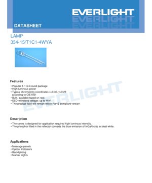
This document details the specifications for a high-luminosity white LED lamp encapsulated in a popular T-1 3/4 round package. The device is engineered using an InGaN semiconductor chip. The blue light emitted by this chip is converted to white light through a phosphor layer deposited within the reflector cup. This design is optimized for applications demanding high brightness and clear visibility.
The core advantages of this LED include its high luminous power output and a compact, industry-standard form factor that facilitates easy integration into existing designs. It is suitable for a broad target market, including industrial control panels, consumer electronics, and signage.
2. Technical Parameter Deep-Dive
2.1 Absolute Maximum Ratings
The device must not be operated beyond these limits to prevent permanent damage.
- Continuous Forward Current (IF): 30 mA
- Peak Forward Current (IFP): 100 mA (Duty Cycle 1/10 @ 1 kHz)
- Reverse Voltage (VR): 5 V
- Power Dissipation (Pd): 110 mW
- Operating Temperature (Topr): -40°C to +85°C
- Storage Temperature (Tstg): -40°C to +100°C
- ESD Withstand (HBM): 4 kV
- Soldering Temperature (Tsol): 260°C for 5 seconds maximum.
2.2 Electro-Optical Characteristics
These parameters are measured at an ambient temperature (Ta) of 25°C under standard test conditions.
- Forward Voltage (VF): 2.8 V (Min), 3.2 V (Typ), 3.6 V (Max) at IF = 20 mA.
- Luminous Intensity (IV): 14250 mcd (Min), Typical value not specified, 28500 mcd (Max) at IF = 20 mA.
- Viewing Angle (2θ1/2): 15 degrees (Typical) at IF = 20 mA.
- Chromaticity Coordinates: x = 0.30 (Typ), y = 0.29 (Typ) according to CIE 1931 standard at IF = 20 mA.
- Reverse Current (IR): 50 μA (Max) at VR = 5V.
- Zener Reverse Voltage (Vz): 5.2 V (Typ) at Iz = 5 mA. This indicates the presence of an integrated protection Zener diode.
3. Binning System Explanation
To ensure consistency in production, LEDs are sorted into bins based on key performance parameters.
3.1 Luminous Intensity Binning
LEDs are categorized into three bins (W, X, Y) based on their minimum and maximum luminous intensity measured at 20 mA.
- Bin W: 14250 mcd to 18000 mcd
- Bin X: 18000 mcd to 22500 mcd
- Bin Y: 22500 mcd to 28500 mcd
The overall tolerance for luminous intensity is ±10%.
3.2 Forward Voltage Binning
LEDs are also binned by forward voltage drop at 20 mA into four groups (0, 1, 2, 3).
- Bin 0: 2.8 V to 3.0 V
- Bin 1: 3.0 V to 3.2 V
- Bin 2: 3.2 V to 3.4 V
- Bin 3: 3.4 V to 3.6 V
The measurement uncertainty for forward voltage is ±0.1V.
3.3 Color Combination
The color output is defined by a specific group. For this product, the designated group is 4, which corresponds to a combination of color ranks A0, B5, and B6. These ranks define specific regions on the CIE chromaticity diagram to ensure the white color point falls within a controlled area.
4. Performance Curve Analysis
The datasheet provides several characteristic curves that are crucial for circuit design and thermal management.
4.1 Relative Intensity vs. Wavelength
This curve shows the spectral power distribution of the white light output. It typically features a primary blue peak from the InGaN chip and a broader yellow phosphor emission, combining to form white light.
4.2 Directivity Pattern
A polar plot illustrating the spatial distribution of light intensity, confirming the narrow 15-degree viewing angle. The pattern shows high intensity directly on-axis, which decreases rapidly at wider angles.
4.3 Forward Current vs. Forward Voltage (I-V Curve)
This graph depicts the exponential relationship between current and voltage, typical of a diode. It is essential for designing the current-limiting circuitry. The curve will show the turn-on voltage and the dynamic resistance in the operating region.
4.4 Relative Intensity vs. Forward Current
This curve shows how light output increases with drive current. It is generally linear within the recommended operating range but may saturate or experience efficiency droop at very high currents.
4.5 Chromaticity Coordinate vs. Forward Current
This plot indicates how the white point (color temperature and tint) may shift with changes in drive current, which is important for color-critical applications.
4.6 Forward Current vs. Ambient Temperature
This derating curve shows the maximum allowable forward current as a function of the ambient temperature. To ensure reliability and prevent overheating, the drive current must be reduced when operating at high temperatures.
5. Mechanical and Package Information
5.1 Package Dimensions
The LED is housed in a T-1 3/4 (5mm) round package with a water-clear resin lens. Key dimensional notes include:
- All dimensions are in millimeters (mm).
- The default tolerance is ±0.25mm unless otherwise specified.
- Lead spacing is measured at the point where the leads exit the package body.
- The maximum protrusion of resin below the flange is 1.5mm.
The dimensional drawing provides exact measurements for the lens diameter, package height, lead length, and lead diameter.
5.2 Polarity Identification
The cathode is typically identified by a flat spot on the rim of the plastic flange or by the shorter lead. The datasheet diagram clearly marks the anode and cathode.
6. Soldering and Assembly Guidelines
Proper handling is critical to maintain LED performance and reliability.
6.1 Lead Forming
- Bending must be done at least 3mm from the base of the epoxy bulb.
- Form leads before soldering.
- Avoid applying stress to the package during bending, as it may cause internal damage or breakage.
- Cut leads at room temperature.
- Ensure PCB holes align perfectly with LED leads to avoid mounting stress.
6.2 Storage Conditions
- Recommended storage: ≤30°C and ≤70% Relative Humidity.
- Shelf life after shipment: 3 months under recommended conditions.
- For longer storage (up to 1 year), use a sealed container with a nitrogen atmosphere and desiccant.
- Avoid rapid temperature changes in humid environments to prevent condensation.
6.3 Soldering Parameters
Maintain a minimum distance of 3mm from the solder joint to the epoxy bulb.
- Hand Soldering: Iron tip temperature ≤300°C (for a 30W max iron), soldering time ≤3 seconds.
- Wave/DIP Soldering: Preheat temperature ≤100°C (for ≤60 sec), solder bath temperature ≤260°C for ≤5 seconds.
7. Packaging and Ordering Information
7.1 Packing Specification
The LEDs are packaged to prevent electrostatic discharge (ESD) and moisture ingress.
- Primary Packing: Anti-static bags.
- Quantity: 200 to 500 pieces per bag.
- Secondary Packing: 5 bags are placed into one inner carton.
- Tertiary Packing: 10 inner cartons are packed into one master (outside) carton.
7.2 Label Explanation
Labels on the packaging contain the following information: Customer's Part Number (CPN), Production Part Number (P/N), Packing Quantity (QTY), Binning Code for Luminous Intensity and Voltage (CAT), Color Rank (HUE), Reference (REF), and Lot Number (LOT No).
7.3 Model Number Designation
The part number 334-15/T1C1-4WYA follows a specific coding structure where elements like the base part number (334-15), package type (T1), chip type/color (C1), and binning codes for color group, luminous intensity, and voltage group are embedded. The exact decoding of the final placeholder codes (represented by squares) would be defined in a full part number key.
8. Application Suggestions
8.1 Typical Application Scenarios
- Message Panels & Signage: Ideal for high-brightness indicator lights in information displays.
- Optical Indicators: Suitable for status lights on industrial equipment, consumer appliances, and automotive dashboards where high visibility is required.
- Backlighting: Can be used for small-scale backlighting of legends, symbols, or small LCD panels.
- Marker Lights: Effective for position or marker lights.
8.2 Design Considerations
- Current Limiting: Always use a series resistor or constant current driver to limit the forward current to a safe value, typically 20 mA for optimal performance and longevity.
- Thermal Management: Although power dissipation is low, ensure adequate ventilation and avoid clustering LEDs tightly on a PCB to prevent localized heating, which can reduce light output and lifespan.
- ESD Protection: While the device has 4kV HBM ESD protection, standard ESD handling precautions should still be observed during assembly.
- Optical Design: The narrow 15-degree viewing angle makes this LED suitable for directed illumination. For wider illumination, secondary optics (like diffusers or lenses) may be required.
9. Technical Comparison and Differentiation
Compared to standard T1 3/4 LEDs, this device offers a significantly higher luminous intensity, making it suitable for applications where superior brightness is needed. The integrated Zener diode for reverse voltage protection is a valuable feature that enhances robustness in circuit designs where voltage spikes or incorrect polarity connection might occur. The specific binning for intensity, voltage, and color provides designers with predictable performance, which is critical for consistency in mass-produced products.
10. Frequently Asked Questions (Based on Technical Parameters)
10.1 What is the recommended operating current?
The electro-optical characteristics are specified at 20 mA, which is the standard test condition and a typical recommended operating point for optimal balance of brightness, efficiency, and reliability.
10.2 Can I drive this LED at 30 mA continuously?
While the absolute maximum continuous current is 30 mA, operating at this limit will generate more heat and may reduce the LED's lifespan. It is generally advised to operate below the maximum, at 20 mA, unless the application's thermal design specifically accounts for the higher power dissipation.
10.3 How do I interpret the color bins A0, B5, B6?
These are codes defining specific quadrilaterals (or regions) on the CIE 1931 chromaticity diagram. LEDs are tested after production, and their color coordinates (x, y) are measured. If the coordinates fall within the defined area for A0, B5, or B6, the LED is assigned to that color rank. Group 4 is a specific mix of LEDs from these three ranks to achieve a desired overall white point characteristic.
10.4 Is a current-limiting resistor necessary?
Yes, absolutely. An LED is a current-driven device. Its forward voltage has a tolerance (2.8V to 3.6V). Connecting it directly to a voltage source like a 3.3V or 5V rail without a series resistor will result in an uncontrolled current that can easily exceed the maximum rating and destroy the LED instantly.
11. Practical Design and Usage Case
Case: Designing a High-Visibility Status Indicator Panel
A designer is creating a control panel for industrial machinery that requires several bright, unambiguous status indicators (e.g., Power On, Fault, Standby). The panel will be viewed from several meters away in a well-lit environment.
Selection Rationale: The high luminous intensity (up to 28,500 mcd) of this LED ensures visibility even in bright ambient light. The narrow 15-degree viewing angle concentrates the light into a beam, making the indicator appear as a distinct point source.
Circuit Design: Each LED is driven by a 5V logic signal through a transistor switch. A series resistor is calculated based on the typical forward voltage (3.2V) and the desired 20 mA current: R = (5V - 3.2V) / 0.02A = 90 Ohms. A standard 91 Ohm, 1/4W resistor is selected. The integrated Zener diode protects the LED if the polarity is accidentally reversed during maintenance.
Layout: LEDs are spaced adequately on the PCB to allow heat dissipation. The leads are inserted into the board, and during wave soldering, the temperature profile is controlled to stay within the 260°C for 5 seconds limit.
12. Operating Principle Introduction
This LED is based on a semiconductor heterostructure made of Indium Gallium Nitride (InGaN). When a forward voltage is applied, electrons and holes recombine in the active region of the chip, releasing energy in the form of photons. The specific composition of the InGaN alloy is tuned to emit blue light with a wavelength around 450-470 nm.
This blue light then strikes a phosphor coating (typically based on Yttrium Aluminum Garnet doped with Cerium, or YAG:Ce) that is deposited inside the reflector cup surrounding the chip. The phosphor absorbs a portion of the blue photons and re-emits light across a broad spectrum in the yellow region. The human eye perceives the mixture of the remaining blue light and the emitted yellow light as white. This method is known as phosphor-converted white LED technology.
13. Technology Trends
The development of white LEDs has been driven by advancements in both chip and phosphor technology. Trends include increasing luminous efficacy (more lumens per watt), improving color rendering index (CRI) for more natural-looking white light, and achieving higher reliability and longer lifetimes. Packaging trends focus on miniaturization, improved thermal management to handle higher power densities, and standardization of footprints for easier design integration. The use of InGaN-based blue chips with advanced phosphor systems remains the dominant and most efficient technology for generating high-intensity white light from solid-state sources.
LED Specification Terminology
Complete explanation of LED technical terms
Photoelectric Performance
| Term | Unit/Representation | Simple Explanation | Why Important |
|---|---|---|---|
| Luminous Efficacy | lm/W (lumens per watt) | Light output per watt of electricity, higher means more energy efficient. | Directly determines energy efficiency grade and electricity cost. |
| Luminous Flux | lm (lumens) | Total light emitted by source, commonly called "brightness". | Determines if the light is bright enough. |
| Viewing Angle | ° (degrees), e.g., 120° | Angle where light intensity drops to half, determines beam width. | Affects illumination range and uniformity. |
| CCT (Color Temperature) | K (Kelvin), e.g., 2700K/6500K | Warmth/coolness of light, lower values yellowish/warm, higher whitish/cool. | Determines lighting atmosphere and suitable scenarios. |
| CRI / Ra | Unitless, 0–100 | Ability to render object colors accurately, Ra≥80 is good. | Affects color authenticity, used in high-demand places like malls, museums. |
| SDCM | MacAdam ellipse steps, e.g., "5-step" | Color consistency metric, smaller steps mean more consistent color. | Ensures uniform color across same batch of LEDs. |
| Dominant Wavelength | nm (nanometers), e.g., 620nm (red) | Wavelength corresponding to color of colored LEDs. | Determines hue of red, yellow, green monochrome LEDs. |
| Spectral Distribution | Wavelength vs intensity curve | Shows intensity distribution across wavelengths. | Affects color rendering and quality. |
Electrical Parameters
| Term | Symbol | Simple Explanation | Design Considerations |
|---|---|---|---|
| Forward Voltage | Vf | Minimum voltage to turn on LED, like "starting threshold". | Driver voltage must be ≥Vf, voltages add up for series LEDs. |
| Forward Current | If | Current value for normal LED operation. | Usually constant current drive, current determines brightness & lifespan. |
| Max Pulse Current | Ifp | Peak current tolerable for short periods, used for dimming or flashing. | Pulse width & duty cycle must be strictly controlled to avoid damage. |
| Reverse Voltage | Vr | Max reverse voltage LED can withstand, beyond may cause breakdown. | Circuit must prevent reverse connection or voltage spikes. |
| Thermal Resistance | Rth (°C/W) | Resistance to heat transfer from chip to solder, lower is better. | High thermal resistance requires stronger heat dissipation. |
| ESD Immunity | V (HBM), e.g., 1000V | Ability to withstand electrostatic discharge, higher means less vulnerable. | Anti-static measures needed in production, especially for sensitive LEDs. |
Thermal Management & Reliability
| Term | Key Metric | Simple Explanation | Impact |
|---|---|---|---|
| Junction Temperature | Tj (°C) | Actual operating temperature inside LED chip. | Every 10°C reduction may double lifespan; too high causes light decay, color shift. |
| Lumen Depreciation | L70 / L80 (hours) | Time for brightness to drop to 70% or 80% of initial. | Directly defines LED "service life". |
| Lumen Maintenance | % (e.g., 70%) | Percentage of brightness retained after time. | Indicates brightness retention over long-term use. |
| Color Shift | Δu′v′ or MacAdam ellipse | Degree of color change during use. | Affects color consistency in lighting scenes. |
| Thermal Aging | Material degradation | Deterioration due to long-term high temperature. | May cause brightness drop, color change, or open-circuit failure. |
Packaging & Materials
| Term | Common Types | Simple Explanation | Features & Applications |
|---|---|---|---|
| Package Type | EMC, PPA, Ceramic | Housing material protecting chip, providing optical/thermal interface. | EMC: good heat resistance, low cost; Ceramic: better heat dissipation, longer life. |
| Chip Structure | Front, Flip Chip | Chip electrode arrangement. | Flip chip: better heat dissipation, higher efficacy, for high-power. |
| Phosphor Coating | YAG, Silicate, Nitride | Covers blue chip, converts some to yellow/red, mixes to white. | Different phosphors affect efficacy, CCT, and CRI. |
| Lens/Optics | Flat, Microlens, TIR | Optical structure on surface controlling light distribution. | Determines viewing angle and light distribution curve. |
Quality Control & Binning
| Term | Binning Content | Simple Explanation | Purpose |
|---|---|---|---|
| Luminous Flux Bin | Code e.g., 2G, 2H | Grouped by brightness, each group has min/max lumen values. | Ensures uniform brightness in same batch. |
| Voltage Bin | Code e.g., 6W, 6X | Grouped by forward voltage range. | Facilitates driver matching, improves system efficiency. |
| Color Bin | 5-step MacAdam ellipse | Grouped by color coordinates, ensuring tight range. | Guarantees color consistency, avoids uneven color within fixture. |
| CCT Bin | 2700K, 3000K etc. | Grouped by CCT, each has corresponding coordinate range. | Meets different scene CCT requirements. |
Testing & Certification
| Term | Standard/Test | Simple Explanation | Significance |
|---|---|---|---|
| LM-80 | Lumen maintenance test | Long-term lighting at constant temperature, recording brightness decay. | Used to estimate LED life (with TM-21). |
| TM-21 | Life estimation standard | Estimates life under actual conditions based on LM-80 data. | Provides scientific life prediction. |
| IESNA | Illuminating Engineering Society | Covers optical, electrical, thermal test methods. | Industry-recognized test basis. |
| RoHS / REACH | Environmental certification | Ensures no harmful substances (lead, mercury). | Market access requirement internationally. |
| ENERGY STAR / DLC | Energy efficiency certification | Energy efficiency and performance certification for lighting. | Used in government procurement, subsidy programs, enhances competitiveness. |