Table of Contents
- 1. Product Overview
- 2. In-Depth Technical Parameter Analysis
- 2.1 Absolute Maximum Ratings
- 2.2 Electro-Optical Characteristics
- 3. Binning System Explanation
- 4. Performance Curve Analysis
- 5. Mechanical and Package Information
- 5.1 Package Dimensions
- 5.2 Pad Configuration and Polarity
- 6. Soldering and Assembly Guidelines
- 6.1 Reflow Soldering Profile
- 6.2 Storage Conditions
- 7. Packaging and Ordering Information
- 8. Application Notes and Design Considerations
- 8.1 Typical Application Circuits
- 8.2 Thermal Management
- 8.3 Optical Design
- 9. Technical Comparison and Differentiation
- 10. Frequently Asked Questions (FAQ)
- 11. Design and Usage Case Study
- 12. Technical Principle Introduction
- 13. Technology Trends
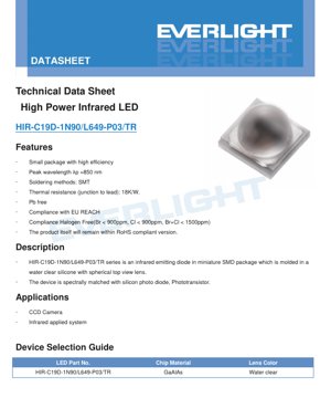
1. Product Overview
The HIR-C19D-1N90/L649-P03/TR is a high-power infrared emitting diode designed for demanding applications requiring robust and efficient infrared illumination. It is housed in a compact surface-mount device (SMD) package, making it suitable for automated assembly processes. The device is molded with a water-clear silicone material featuring a spherical top lens, which aids in achieving its specified viewing angle and radiant intensity profile.
The core advantage of this LED lies in its combination of a small form factor and high optical output efficiency. It is constructed using a GaAlAs (Gallium Aluminum Arsenide) chip material, which is optimized for emission in the near-infrared spectrum. A key feature is its spectral match with silicon photodiodes and phototransistors, making it an ideal light source for sensing and imaging systems that utilize these common silicon-based detectors. This ensures maximum responsivity and signal-to-noise ratio in the target application.
The primary target markets and applications include surveillance and security systems, particularly CCD-based cameras for night vision, and various infrared-applied systems such as proximity sensors, industrial automation, and machine vision. Its compliance with environmental standards like RoHS, REACH, and halogen-free requirements makes it suitable for use in products with strict regulatory demands.
2. In-Depth Technical Parameter Analysis
2.1 Absolute Maximum Ratings
The device is rated for a continuous forward current (IF) of 1500 mA. For pulsed operation, it can handle a peak forward current (IFP) of 5000 mA under specific conditions (pulse width ≤100μs, duty cycle ≤1%). The maximum reverse voltage (VR) is 5V, which is a typical value for LEDs and indicates the device should not be subjected to significant reverse bias. The operating and storage temperature range is specified from -40°C to +100°C, with a maximum junction temperature (Tj) of 125°C. Exceeding these ratings may cause permanent damage.
The thermal resistance from the junction to the lead frame (Rth(j-L)) is 18 K/W. This parameter is critical for thermal management. It defines how much the junction temperature rises for every watt of power dissipated. With a specified power dissipation (Pd) of 3W at IF=700mA, effective heat sinking is essential to maintain the junction temperature within safe limits, especially at higher drive currents.
2.2 Electro-Optical Characteristics
The primary optical parameters are measured at a standard ambient temperature of 25°C. The peak wavelength (λp) is 850 nm, which is in the near-infrared region and invisible to the human eye but highly detectable by silicon sensors. The spectral bandwidth (Δλ) is typically 25 nm, indicating the spectral purity of the emitted light.
The radiant performance scales with drive current:
- At IF=350 mA: Total Radiated Power (Po) is 500 mW (typ), Radiant Intensity (IE) is 200 mW/sr (typ).
- At IF=700 mA: Po is 900 mW (typ), IE is 400 mW/sr (typ).
- At IF=1 A: Po is 1300 mW (typ), IE is 560 mW/sr (typ).
The forward voltage (VF) increases with current due to the diode's inherent resistance:
- 3.0V (typ) at 350 mA.
- 3.3V (typ) at 700 mA.
- 3.5V (typ) at 1 A.
- 3.8V (typ) at 5 A (pulsed).
The reverse current (IR) is a maximum of 10 μA at VR=5V. The viewing angle (2θ1/2), defined as the full angle at half intensity, is 90 degrees, providing a relatively wide beam pattern suitable for area illumination.
3. Binning System Explanation
The product utilizes a binning system for Total Radiated Power measured at a drive current of 1000 mA (1A). This system categorizes LEDs based on their optical output to ensure consistency in application performance. The bin codes and their corresponding power ranges (including a ±10% test tolerance) are:
- Bin G: Minimum 800 mW, Maximum 1260 mW.
- Bin H: Minimum 1000 mW, Maximum 1600 mW.
- Bin I: Minimum 1260 mW, Maximum 2000 mW.
This allows designers to select components that meet specific minimum brightness requirements for their system. The datasheet does not indicate separate bins for wavelength or forward voltage for this specific part number, suggesting tight control over these parameters in manufacturing.
4. Performance Curve Analysis
The datasheet references several typical characteristic curves which are crucial for understanding device behavior under different operating conditions.
Forward Current vs. Forward Voltage (Fig.1): This IV curve shows the exponential relationship typical of a diode. It is essential for designing the current drive circuit and calculating power consumption (VF * IF). The curve will shift with temperature.
Forward Current vs. Radiant Intensity / Total Power (Fig.2 & Fig.3): These graphs illustrate the light output as a function of drive current. The relationship is generally linear at lower currents but may show signs of efficiency droop (sub-linear increase) at very high currents due to thermal and electrical effects. This helps in selecting the optimal operating point for balancing output and efficiency/heat.
Relative Radiant Intensity vs. Angular Displacement (Fig.4): This polar plot defines the spatial radiation pattern. The 90-degree viewing angle is confirmed here. The shape of the curve (e.g., Lambertian, batwing) impacts how light is distributed over the target area.
Forward Current vs. Ambient Temperature (Fig.5): This derating curve is one of the most critical for reliability. It shows the maximum allowable forward current to keep the junction temperature below 125°C as the ambient temperature increases. At 100°C ambient, the allowable continuous current is significantly reduced. This graph must be used for any design operating in a non-25°C environment.
5. Mechanical and Package Information
5.1 Package Dimensions
The LED is housed in a surface-mount package. Key dimensions from the drawing include the body size, lens height, and lead spacing. Tolerances are typically ±0.1mm unless otherwise noted. A critical handling note warns against applying force to the lens, as this can damage the internal structure and lead to device failure. The device should be handled by its body or leads during assembly.
5.2 Pad Configuration and Polarity
The device has three electrical pads: Pad 1 is the Anode (+), Pad 2 is the Cathode (-), and Pad P is a dedicated Thermal Pad. The thermal pad is crucial for transferring heat from the LED junction to the printed circuit board (PCB). For optimal thermal and electrical performance, the PCB layout must include a properly sized copper pour connected to this pad, with thermal vias to inner or bottom layers if necessary. Correct polarity connection (Anode to positive supply) is mandatory for operation.
6. Soldering and Assembly Guidelines
6.1 Reflow Soldering Profile
The device is suitable for standard SMT reflow processes. A lead-free reflow profile is provided:
- Ramp-Up Rate: 2~3 °C/sec.
- Preheat: 150~200°C for 60~120 seconds.
- Liquidous Temperature (TL): 217°C.
- Time Above TL: 60~90 seconds.
- Peak Temperature (TP): 240 ±5°C.
- Time at Peak (tP): Maximum 20 seconds.
- Ramp-Down Rate: 3~5 °C/sec.
It is recommended that reflow soldering not be performed more than twice to minimize thermal stress on the package and internal bonds. Stress on the LED during heating should be avoided, and the circuit board should not be bent after soldering to prevent mechanical damage to the solder joints or the LED itself.
6.2 Storage Conditions
The device is shipped in moisture-resistant packaging, including an aluminum moisture-proof bag with desiccant. If the packaging is opened, the devices are sensitive to moisture absorption and should be used within a specified time or baked according to standard MSL (Moisture Sensitivity Level) procedures before reflow to prevent "popcorning" damage during soldering. The specific MSL level is not stated in the provided excerpt.
7. Packaging and Ordering Information
The device is supplied on carrier tape and reel for automated pick-and-place assembly. Each reel contains 400 pieces. The carrier tape dimensions are provided to ensure compatibility with feeder equipment. The packaging label includes standard information such as Part Number (P/N), quantity (QTY), and lot number (LOT No.) for traceability. The bin code for radiant power (CAT) would also be indicated here.
8. Application Notes and Design Considerations
8.1 Typical Application Circuits
This infrared LED requires a constant current source for stable operation, not a constant voltage. A simple series resistor can be used for low-current applications, but for the high currents this device is capable of, a dedicated LED driver IC or transistor-based current regulator is recommended to ensure consistent light output and protect the LED from current spikes. The driver must be capable of supplying up to the required forward current and handling the forward voltage drop.
8.2 Thermal Management
This is the most critical aspect of using this high-power LED. The datasheet explicitly suggests adding a heat sink. The PCB design must incorporate a significant thermal pad connected to the LED's thermal pad with ample copper area. The use of thermal vias to conduct heat to other PCB layers or an external heatsink is highly recommended. The maximum junction temperature of 125°C must not be exceeded; therefore, thermal calculations or measurements should be performed based on the actual operating current, ambient temperature, and PCB thermal properties.
8.3 Optical Design
For applications like camera illumination, secondary optics (lenses or reflectors) may be used to collimate or shape the 90-degree beam into a more focused pattern to increase throw distance or efficiency. The water-clear lens ensures minimal absorption of the infrared light. Designers should consider the radiant intensity (mW/sr) rather than just total power when designing for illumination at a distance.
9. Technical Comparison and Differentiation
Compared to standard 5mm or 3mm through-hole infrared LEDs, this SMD device offers significantly higher optical power output (up to 1300+ mW vs. tens of mW) in a more compact and manufacturable package. Its 18 K/W thermal resistance is relatively low for an SMD LED, indicating a good thermal path, but still requires careful management compared to LEDs mounted on metal-core PCBs or with integrated heatsinks. The 850nm wavelength is a common standard, offering a good balance between silicon detector sensitivity and lower visibility compared to 940nm LEDs (which are nearly invisible but produce lower sensor response).
10. Frequently Asked Questions (FAQ)
Q: Can I drive this LED directly from a 5V supply with a resistor?
A: Possibly, but it requires careful calculation. At 1A, VF is ~3.5V. A series resistor would need to drop 1.5V at 1A, meaning R = 1.5Ω and it would dissipate 1.5W. This is inefficient and creates more heat. A dedicated current regulator is strongly preferred for currents above 350mA.
Q: Why is a heat sink necessary?
A: At 700mA, power dissipation is approximately 3.3V * 0.7A = 2.31W. With an 18 K/W thermal resistance, the junction would rise 2.31W * 18 K/W = ~41.6°C above the lead temperature. If the PCB/lead isn't cooled, the junction can easily exceed 125°C, leading to rapid degradation or failure.
Q: What is the difference between Total Radiated Power (mW) and Radiant Intensity (mW/sr)?
A: Total Radiant Power is the integrated optical power emitted in all directions. Radiant Intensity is the power emitted per unit solid angle in a specific direction (typically on-axis). Intensity is more relevant for directed applications, while total power matters for overall system efficiency.
Q: Is this LED safe for eye exposure?
A: Infrared LEDs, especially high-power ones, can be hazardous to eyes. They emit invisible radiation that can cause retinal damage before the blink reflex engages. Always follow relevant laser/infrared product safety standards (like IEC 62471) and implement appropriate safeguards (diffusers, enclosures, intensity limits) in the final product.
11. Design and Usage Case Study
Scenario: Night Vision Illumination for a Security Camera.
A designer is creating a compact IP camera with night vision capability using a silicon-based image sensor. They select this 850nm LED for its high output and spectral match. Four LEDs are placed around the camera lens. Each is driven at 700mA by a compact switching LED driver IC to ensure stable output as battery voltage changes. The PCB is a 4-layer board with the inner ground plane connected via multiple thermal vias to the large copper pad under each LED for heat spreading. A slight diffuser film is placed over the LEDs to blend the beams and reduce hotspots in the image. The thermal design is validated with a thermal camera, confirming the LED case temperature stays below 85°C in a 40°C ambient environment, keeping the junction safely below its limit. The resulting system provides clear, evenly illuminated night vision footage up to 30 meters.
12. Technical Principle Introduction
Infrared LEDs operate on the same fundamental principle as visible LEDs: electroluminescence in a semiconductor p-n junction. When a forward voltage is applied, electrons and holes are injected into the active region where they recombine, releasing energy in the form of photons. The wavelength (color) of the emitted light is determined by the bandgap energy of the semiconductor material. GaAlAs (Gallium Aluminum Arsenide) is a compound semiconductor whose bandgap can be tuned by varying the Aluminum content to emit in the near-infrared range, specifically around 850nm. The water-clear silicone encapsulation is transparent to this wavelength and is formed into a lens to shape the output beam. The high-power capability is achieved by using a larger semiconductor die and an efficient package designed to extract heat.
13. Technology Trends
The trend in infrared LEDs, particularly for sensing and imaging, is towards higher efficiency (more radiant power per electrical watt), which reduces heat generation and power consumption. This is achieved through advances in epitaxial layer design and light extraction techniques. There is also a move towards tighter integration, such as LEDs with built-in drivers or combined with photodetectors in a single package. Wavelengths like 940nm are gaining popularity for "covert" illumination as they are less visible to the human eye than 850nm, though they require sensors with higher sensitivity. Furthermore, the drive for miniaturization continues, pushing for high power in ever-smaller SMD packages, which in turn increases the importance of advanced thermal management solutions at the PCB and system level.
LED Specification Terminology
Complete explanation of LED technical terms
Photoelectric Performance
| Term | Unit/Representation | Simple Explanation | Why Important |
|---|---|---|---|
| Luminous Efficacy | lm/W (lumens per watt) | Light output per watt of electricity, higher means more energy efficient. | Directly determines energy efficiency grade and electricity cost. |
| Luminous Flux | lm (lumens) | Total light emitted by source, commonly called "brightness". | Determines if the light is bright enough. |
| Viewing Angle | ° (degrees), e.g., 120° | Angle where light intensity drops to half, determines beam width. | Affects illumination range and uniformity. |
| CCT (Color Temperature) | K (Kelvin), e.g., 2700K/6500K | Warmth/coolness of light, lower values yellowish/warm, higher whitish/cool. | Determines lighting atmosphere and suitable scenarios. |
| CRI / Ra | Unitless, 0–100 | Ability to render object colors accurately, Ra≥80 is good. | Affects color authenticity, used in high-demand places like malls, museums. |
| SDCM | MacAdam ellipse steps, e.g., "5-step" | Color consistency metric, smaller steps mean more consistent color. | Ensures uniform color across same batch of LEDs. |
| Dominant Wavelength | nm (nanometers), e.g., 620nm (red) | Wavelength corresponding to color of colored LEDs. | Determines hue of red, yellow, green monochrome LEDs. |
| Spectral Distribution | Wavelength vs intensity curve | Shows intensity distribution across wavelengths. | Affects color rendering and quality. |
Electrical Parameters
| Term | Symbol | Simple Explanation | Design Considerations |
|---|---|---|---|
| Forward Voltage | Vf | Minimum voltage to turn on LED, like "starting threshold". | Driver voltage must be ≥Vf, voltages add up for series LEDs. |
| Forward Current | If | Current value for normal LED operation. | Usually constant current drive, current determines brightness & lifespan. |
| Max Pulse Current | Ifp | Peak current tolerable for short periods, used for dimming or flashing. | Pulse width & duty cycle must be strictly controlled to avoid damage. |
| Reverse Voltage | Vr | Max reverse voltage LED can withstand, beyond may cause breakdown. | Circuit must prevent reverse connection or voltage spikes. |
| Thermal Resistance | Rth (°C/W) | Resistance to heat transfer from chip to solder, lower is better. | High thermal resistance requires stronger heat dissipation. |
| ESD Immunity | V (HBM), e.g., 1000V | Ability to withstand electrostatic discharge, higher means less vulnerable. | Anti-static measures needed in production, especially for sensitive LEDs. |
Thermal Management & Reliability
| Term | Key Metric | Simple Explanation | Impact |
|---|---|---|---|
| Junction Temperature | Tj (°C) | Actual operating temperature inside LED chip. | Every 10°C reduction may double lifespan; too high causes light decay, color shift. |
| Lumen Depreciation | L70 / L80 (hours) | Time for brightness to drop to 70% or 80% of initial. | Directly defines LED "service life". |
| Lumen Maintenance | % (e.g., 70%) | Percentage of brightness retained after time. | Indicates brightness retention over long-term use. |
| Color Shift | Δu′v′ or MacAdam ellipse | Degree of color change during use. | Affects color consistency in lighting scenes. |
| Thermal Aging | Material degradation | Deterioration due to long-term high temperature. | May cause brightness drop, color change, or open-circuit failure. |
Packaging & Materials
| Term | Common Types | Simple Explanation | Features & Applications |
|---|---|---|---|
| Package Type | EMC, PPA, Ceramic | Housing material protecting chip, providing optical/thermal interface. | EMC: good heat resistance, low cost; Ceramic: better heat dissipation, longer life. |
| Chip Structure | Front, Flip Chip | Chip electrode arrangement. | Flip chip: better heat dissipation, higher efficacy, for high-power. |
| Phosphor Coating | YAG, Silicate, Nitride | Covers blue chip, converts some to yellow/red, mixes to white. | Different phosphors affect efficacy, CCT, and CRI. |
| Lens/Optics | Flat, Microlens, TIR | Optical structure on surface controlling light distribution. | Determines viewing angle and light distribution curve. |
Quality Control & Binning
| Term | Binning Content | Simple Explanation | Purpose |
|---|---|---|---|
| Luminous Flux Bin | Code e.g., 2G, 2H | Grouped by brightness, each group has min/max lumen values. | Ensures uniform brightness in same batch. |
| Voltage Bin | Code e.g., 6W, 6X | Grouped by forward voltage range. | Facilitates driver matching, improves system efficiency. |
| Color Bin | 5-step MacAdam ellipse | Grouped by color coordinates, ensuring tight range. | Guarantees color consistency, avoids uneven color within fixture. |
| CCT Bin | 2700K, 3000K etc. | Grouped by CCT, each has corresponding coordinate range. | Meets different scene CCT requirements. |
Testing & Certification
| Term | Standard/Test | Simple Explanation | Significance |
|---|---|---|---|
| LM-80 | Lumen maintenance test | Long-term lighting at constant temperature, recording brightness decay. | Used to estimate LED life (with TM-21). |
| TM-21 | Life estimation standard | Estimates life under actual conditions based on LM-80 data. | Provides scientific life prediction. |
| IESNA | Illuminating Engineering Society | Covers optical, electrical, thermal test methods. | Industry-recognized test basis. |
| RoHS / REACH | Environmental certification | Ensures no harmful substances (lead, mercury). | Market access requirement internationally. |
| ENERGY STAR / DLC | Energy efficiency certification | Energy efficiency and performance certification for lighting. | Used in government procurement, subsidy programs, enhances competitiveness. |