Table of Contents
- 1. Product Overview
- 1.1 Target Applications
- 2. Technical Specifications and Objective Interpretation
- 2.1 Absolute Maximum Ratings
- 2.2 Electro-Optical Characteristics
- 2.3 Thermal Characteristics
- 3. Binning System Explanation
- 4. Performance Curve Analysis
- 4.1 Forward Current vs. Forward Voltage (IV Curve)
- 4.2 Forward Current vs. Radiant Intensity/Power
- 4.3 Relative Radiant Intensity vs. Angular Displacement
- 4.4 Forward Current vs. Ambient Temperature
- 5. Mechanical and Package Information
- 5.1 Package Dimensions
- 5.2 Pad Configuration and Polarity Identification
- 6. Soldering and Assembly Guidelines
- 6.1 Reflow Soldering Profile
- 6.2 Critical Assembly Notes
- 7. Packaging and Ordering Information
- 7.1 Tape and Reel Specifications
- 7.2 Moisture-Sensitive Packaging
- 8. Application Recommendations and Design Considerations
- 8.1 Driver Circuit Design
- 8.2 Thermal Management Design
- 8.3 Optical Design
- 9. Technical Comparison and Differentiation
- 10. Frequently Asked Questions (Based on Technical Parameters)
- 10.1 What is the difference between Radiant Power and Radiant Intensity?
- 10.2 Can I drive this LED directly from a voltage source?
- 10.3 Why is heatsinking so strongly emphasized?
- 10.4 What does the Bin Code mean for my design?
- 11. Practical Design and Usage Case Study
- 12. Operational Principle
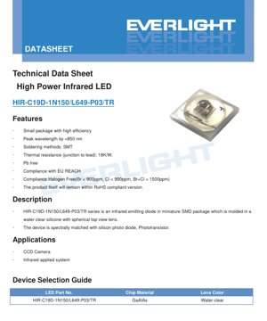
1. Product Overview
The HIR-C19D-1N150/L649-P03/TR is a high-power infrared emitting diode designed for demanding illumination applications. It features a miniature surface-mount device (SMD) package with a water-clear silicone encapsulation and a spherical top lens, optimizing light extraction and radiation pattern. The device's spectral output is centered at 850nm, making it ideally matched with silicon photodiodes and phototransistors for sensing and imaging systems. Its core advantages include high radiant output from a compact form factor, excellent thermal management characteristics, and compliance with modern environmental and safety standards such as RoHS, REACH, and halogen-free requirements.
1.1 Target Applications
This infrared LED is primarily targeted at applications requiring robust, invisible illumination. Its key application areas include surveillance and security systems, where it is used to provide night-time illumination for CCD cameras. It is also suitable for various infrared-based systems such as proximity sensors, gesture recognition modules, and industrial machine vision. The high radiant power enables longer-range illumination or coverage of wider areas compared to standard infrared LEDs.
2. Technical Specifications and Objective Interpretation
The device's performance is defined under standard test conditions (TA=25°C). A detailed, objective analysis of its key parameters is provided below.
2.1 Absolute Maximum Ratings
These ratings define the stress limits beyond which permanent damage to the device may occur. They are not intended for normal operation.
- Continuous Forward Current (IF): 1500 mA. This is the maximum DC current that can be applied indefinitely without exceeding the junction temperature limit.
- Peak Forward Current (IFP): 5000 mA. This high current is permissible only under pulsed conditions (pulse width ≤100μs, duty cycle ≤1%), useful for short-burst, high-intensity illumination.
- Reverse Voltage (VR): 5 V. Exceeding this voltage in reverse bias can cause junction breakdown.
- Junction Temperature (Tj): 115 °C. The maximum allowable temperature at the semiconductor junction.
- Power Dissipation (Pd): 3 W at IF=700mA. This indicates the device's ability to handle heat generation at a specific operating point.
2.2 Electro-Optical Characteristics
These parameters define the light output and electrical behavior under typical operating conditions.
- Total Radiated Power (Po): The optical power emitted in all directions. At 1A drive current, the typical value ranges from 900mW to 1100mW, indicating high efficiency.
- Radiant Intensity (IE): The optical power per solid angle, measured in mW/sr. At 1A, it is typically between 230 and 270 mW/sr. This metric is relevant for directed beam applications.
- Peak Wavelength (λP): 850 nm. This is the wavelength at which the spectral output is strongest, perfectly aligned with the peak sensitivity of silicon-based detectors.
- Spectral Bandwidth (Δλ): 25 nm. This defines the range of wavelengths emitted, typically the full width at half maximum (FWHM).
- Forward Voltage (VF): Typically 3.10V at 1A. This is the voltage drop across the LED when operating, crucial for driver design and power dissipation calculations.
- View Angle (2θ1/2): 150 degrees. This very wide viewing angle provides broad, diffuse illumination rather than a narrow spotlight, ideal for area coverage.
2.3 Thermal Characteristics
Effective thermal management is critical for high-power LEDs to maintain performance and longevity.
- Thermal Resistance (Rth(j-L)): 18 K/W (junction to lead frame). This low value indicates good internal heat transfer from the chip to the package leads, but external heatsinking is strongly recommended for operation at high currents.
3. Binning System Explanation
The device is sorted (binned) based on its radiant power output at a standard test current of 1000mA. This ensures consistency in application performance.
- Bin F: Radiant Power from 640 mW to 1000 mW.
- Bin G: Radiant Power from 800 mW to 1260 mW.
- Bin H: Radiant Power from 1000 mW to 1600 mW.
The bin code allows designers to select LEDs with guaranteed minimum output for their specific application needs. All measurements include a ±10% test tolerance.
4. Performance Curve Analysis
The datasheet provides several characteristic curves that are essential for understanding device behavior under varying conditions.
4.1 Forward Current vs. Forward Voltage (IV Curve)
This curve shows the non-linear relationship between current and voltage. It is essential for designing the current-limiting circuitry. The curve will show a threshold voltage (around 1.2V for GaAlAs) after which current increases rapidly with a small increase in voltage.
4.2 Forward Current vs. Radiant Intensity/Power
These curves demonstrate the light output's dependence on drive current. Typically, the output increases super-linearly at lower currents and then tends to saturate at higher currents due to thermal effects and efficiency droop. The curves provided for this device at 350mA, 700mA, and 1A illustrate this trend.
4.3 Relative Radiant Intensity vs. Angular Displacement
This polar plot visualizes the 150-degree view angle. It shows the radiation pattern, which is nearly Lambertian (cosine distribution) due to the spherical lens, providing uniform illumination over a wide area.
4.4 Forward Current vs. Ambient Temperature
This graph is critical for derating. It shows how the maximum allowable forward current must be reduced as the ambient temperature increases to prevent the junction temperature from exceeding its 115°C limit. This curve directly informs thermal design and heatsink requirements.
5. Mechanical and Package Information
5.1 Package Dimensions
The device is housed in a compact 5.0mm x 5.0mm SMD package with a height of 1.9mm. The lens is a prominent spherical dome. Critical dimensional tolerances are ±0.1mm unless otherwise specified. A specific warning is given not to handle the device by the lens, as mechanical stress can cause failure.
5.2 Pad Configuration and Polarity Identification
The package has three pads: Pad 1 (Anode), Pad 2 (Cathode), and a large central thermal pad (P). The thermal pad is crucial for transferring heat from the LED die to the printed circuit board (PCB). The pad layout diagram clearly shows the anode and cathode positions for correct electrical connection.
6. Soldering and Assembly Guidelines
6.1 Reflow Soldering Profile
The device is suitable for standard lead-free SMT reflow processes. The recommended profile is as follows:
- Ramp-Up Rate: 2–3 °C/sec
- Preheat: 150–200 °C for 60–120 seconds
- Time Above Liquidus (TL=217°C): 60–90 seconds
- Peak Temperature (TP): 240 ±5 °C
- Time within 5°C of Peak: Maximum 20 seconds
- Ramp-Down Rate: 3–5 °C/sec
6.2 Critical Assembly Notes
- Reflow soldering should not be performed more than twice to avoid excessive thermal stress on the package and wire bonds.
- Mechanical stress on the LED during heating (e.g., from board flexure) must be avoided.
- The PCB should not be bent after soldering, as this can crack the solder joints or the LED package itself.
- Adequate heatsinking, as suggested in the notes, is mandatory for reliable operation at high currents.
7. Packaging and Ordering Information
7.1 Tape and Reel Specifications
The devices are supplied on carrier tape and reel for automated assembly. Each reel contains 400 pieces. Detailed carrier tape and reel dimensions are provided to ensure compatibility with pick-and-place equipment.
7.2 Moisture-Sensitive Packaging
The product is packaged in a moisture-resistant aluminum bag with a desiccant to protect it from ambient humidity during storage and transport, which is standard practice for SMD components.
8. Application Recommendations and Design Considerations
8.1 Driver Circuit Design
Due to the high forward current (up to 1.5A continuous), a constant-current driver is essential. The driver must be capable of supplying the required current while withstanding the forward voltage drop (approx. 3.1V at 1A). Switching regulators are often preferred over linear regulators for efficiency at these power levels. The driver design must also incorporate thermal protection or current derating based on the ambient temperature curve.
8.2 Thermal Management Design
This is the most critical aspect of using this high-power LED. The low junction-to-lead thermal resistance (18K/W) is only part of the system. The total thermal path from junction to ambient (Rth(j-A)) must be minimized. This involves:
- Using a PCB with a thermal via array under the thermal pad connected to large copper planes or an internal ground layer.
- Possibly attaching an external heatsink to the PCB.
- Ensuring good airflow in the end application.
- Using thermal interface material if necessary.
The maximum junction temperature of 115°C must never be exceeded. The derating curve (Forward Current vs. Ambient Temperature) provides the necessary data to calculate the required heatsink performance.
8.3 Optical Design
The 150-degree viewing angle provides wide coverage. For applications requiring a more focused beam, secondary optics (lenses or reflectors) can be used. The 850nm wavelength is invisible to the human eye but easily detectable by silicon sensors and most CCD/CMOS cameras, which often have an infrared cut filter that must be removed or replaced with one that passes 850nm for effective use.
9. Technical Comparison and Differentiation
Compared to standard 5mm or 3mm through-hole infrared LEDs, this device offers significantly higher radiant output (by an order of magnitude or more) in a surface-mount package, enabling more compact and robust designs. Its key differentiators are its combination of high power (up to 3W dissipation), wide viewing angle, and the integrated thermal pad for effective heat dissipation—a feature often missing in lower-power SMD LEDs. The use of GaAlAs chip material is standard for high-efficiency infrared emitters in this wavelength range.
10. Frequently Asked Questions (Based on Technical Parameters)
10.1 What is the difference between Radiant Power and Radiant Intensity?
Radiant Power (Po, in mW) is the total optical power emitted in all directions. Radiant Intensity (IE, in mW/sr) is the power emitted per unit solid angle in a specific direction. For a wide-angle LED like this one, the total power is high, but the intensity in any single direction is lower than a narrow-beam LED with the same total power.
10.2 Can I drive this LED directly from a voltage source?
No. LEDs are current-driven devices. Their forward voltage has a tolerance and varies with temperature. Connecting directly to a voltage source will cause an uncontrolled current to flow, likely exceeding the maximum rating and destroying the LED. A constant-current driver or a current-limiting circuit is mandatory.
10.3 Why is heatsinking so strongly emphasized?
High-power LEDs convert a significant portion of electrical input into heat. If this heat is not effectively removed, the junction temperature rises. High junction temperatures lead to reduced light output (efficiency droop), accelerated degradation of the semiconductor materials, and ultimately catastrophic failure. Proper thermal design ensures performance, reliability, and longevity.
10.4 What does the Bin Code mean for my design?
Selecting a higher bin (e.g., Bin H over Bin F) guarantees a higher minimum radiant output. This allows you to design your system with a known, guaranteed level of illumination. If your design has ample margin, a lower bin may be more cost-effective. If you are pushing the limits of illumination range or camera sensitivity, a higher bin is necessary.
11. Practical Design and Usage Case Study
Scenario: Designing an IR Illuminator for a Security Camera
A designer needs to create a compact, wall-mounted IR illuminator to extend the night-vision range of a security camera from 10 meters to 25 meters. The camera's sensor is sensitive to 850nm. The designer selects the HIR-C19D-1N150/L649-P03/TR LED in Bin H for maximum output.
Design Steps:
- Electrical Design: A switching constant-current driver is designed to provide 1000mA to the LED from a 12V DC supply. The driver includes over-current and thermal shutdown protection.
- Thermal Design: A 2-layer PCB is used with a 2oz copper weight. An array of thermal vias connects the LED's thermal pad to a large bottom copper pour, which acts as a heatsink. The enclosure is made of aluminum with the PCB mounted directly to it using thermal paste to further dissipate heat.
- Optical/Mechanical Design: Four LEDs are arranged in a square pattern on the PCB. A flat, clear polycarbonate window protects the LEDs. The wide 150-degree beam of each LED overlaps to create a uniform flood of infrared light covering the camera's field of view at the desired range.
- Validation: The prototype is tested in a dark room. A thermal camera confirms the LED junction temperatures remain below 100°C. The security camera successfully identifies objects at 25 meters with clear contrast.
This case highlights the interdependence of driver design, thermal management, and optical layout when utilizing this high-power component.
12. Operational Principle
The HIR-C19D-1N150/L649-P03/TR is a semiconductor light source based on a Gallium Aluminum Arsenide (GaAlAs) heterostructure. When a forward voltage exceeding the diode's bandgap energy is applied, electrons and holes are injected into the active region where they recombine. This recombination process releases energy in the form of photons. The specific composition of the GaAlAs layers determines the bandgap energy, which in turn defines the peak wavelength of the emitted photons—in this case, 850 nanometers, which is in the near-infrared spectrum. The water-clear silicone encapsulation protects the semiconductor chip and acts as a primary optical element, with its spherical shape helping to extract light efficiently and shape the radiation pattern.
13. Technology Trends
The field of high-power infrared LEDs continues to evolve with several clear trends. There is a constant drive for higher wall-plug efficiency (optical power out / electrical power in) to reduce heat generation and energy consumption for the same light output. This involves advancements in epitaxial growth techniques and chip design. Package technology is also improving to offer lower thermal resistance, allowing more heat to be extracted from the chip. Furthermore, there is growing integration, with drivers and sometimes even simple control logic being co-packaged with the LED die to create smarter, easier-to-use illumination modules. The demand for reliable, high-power infrared sources is sustained by expanding applications in automotive LiDAR, facial recognition, and advanced industrial automation.
LED Specification Terminology
Complete explanation of LED technical terms
Photoelectric Performance
| Term | Unit/Representation | Simple Explanation | Why Important |
|---|---|---|---|
| Luminous Efficacy | lm/W (lumens per watt) | Light output per watt of electricity, higher means more energy efficient. | Directly determines energy efficiency grade and electricity cost. |
| Luminous Flux | lm (lumens) | Total light emitted by source, commonly called "brightness". | Determines if the light is bright enough. |
| Viewing Angle | ° (degrees), e.g., 120° | Angle where light intensity drops to half, determines beam width. | Affects illumination range and uniformity. |
| CCT (Color Temperature) | K (Kelvin), e.g., 2700K/6500K | Warmth/coolness of light, lower values yellowish/warm, higher whitish/cool. | Determines lighting atmosphere and suitable scenarios. |
| CRI / Ra | Unitless, 0–100 | Ability to render object colors accurately, Ra≥80 is good. | Affects color authenticity, used in high-demand places like malls, museums. |
| SDCM | MacAdam ellipse steps, e.g., "5-step" | Color consistency metric, smaller steps mean more consistent color. | Ensures uniform color across same batch of LEDs. |
| Dominant Wavelength | nm (nanometers), e.g., 620nm (red) | Wavelength corresponding to color of colored LEDs. | Determines hue of red, yellow, green monochrome LEDs. |
| Spectral Distribution | Wavelength vs intensity curve | Shows intensity distribution across wavelengths. | Affects color rendering and quality. |
Electrical Parameters
| Term | Symbol | Simple Explanation | Design Considerations |
|---|---|---|---|
| Forward Voltage | Vf | Minimum voltage to turn on LED, like "starting threshold". | Driver voltage must be ≥Vf, voltages add up for series LEDs. |
| Forward Current | If | Current value for normal LED operation. | Usually constant current drive, current determines brightness & lifespan. |
| Max Pulse Current | Ifp | Peak current tolerable for short periods, used for dimming or flashing. | Pulse width & duty cycle must be strictly controlled to avoid damage. |
| Reverse Voltage | Vr | Max reverse voltage LED can withstand, beyond may cause breakdown. | Circuit must prevent reverse connection or voltage spikes. |
| Thermal Resistance | Rth (°C/W) | Resistance to heat transfer from chip to solder, lower is better. | High thermal resistance requires stronger heat dissipation. |
| ESD Immunity | V (HBM), e.g., 1000V | Ability to withstand electrostatic discharge, higher means less vulnerable. | Anti-static measures needed in production, especially for sensitive LEDs. |
Thermal Management & Reliability
| Term | Key Metric | Simple Explanation | Impact |
|---|---|---|---|
| Junction Temperature | Tj (°C) | Actual operating temperature inside LED chip. | Every 10°C reduction may double lifespan; too high causes light decay, color shift. |
| Lumen Depreciation | L70 / L80 (hours) | Time for brightness to drop to 70% or 80% of initial. | Directly defines LED "service life". |
| Lumen Maintenance | % (e.g., 70%) | Percentage of brightness retained after time. | Indicates brightness retention over long-term use. |
| Color Shift | Δu′v′ or MacAdam ellipse | Degree of color change during use. | Affects color consistency in lighting scenes. |
| Thermal Aging | Material degradation | Deterioration due to long-term high temperature. | May cause brightness drop, color change, or open-circuit failure. |
Packaging & Materials
| Term | Common Types | Simple Explanation | Features & Applications |
|---|---|---|---|
| Package Type | EMC, PPA, Ceramic | Housing material protecting chip, providing optical/thermal interface. | EMC: good heat resistance, low cost; Ceramic: better heat dissipation, longer life. |
| Chip Structure | Front, Flip Chip | Chip electrode arrangement. | Flip chip: better heat dissipation, higher efficacy, for high-power. |
| Phosphor Coating | YAG, Silicate, Nitride | Covers blue chip, converts some to yellow/red, mixes to white. | Different phosphors affect efficacy, CCT, and CRI. |
| Lens/Optics | Flat, Microlens, TIR | Optical structure on surface controlling light distribution. | Determines viewing angle and light distribution curve. |
Quality Control & Binning
| Term | Binning Content | Simple Explanation | Purpose |
|---|---|---|---|
| Luminous Flux Bin | Code e.g., 2G, 2H | Grouped by brightness, each group has min/max lumen values. | Ensures uniform brightness in same batch. |
| Voltage Bin | Code e.g., 6W, 6X | Grouped by forward voltage range. | Facilitates driver matching, improves system efficiency. |
| Color Bin | 5-step MacAdam ellipse | Grouped by color coordinates, ensuring tight range. | Guarantees color consistency, avoids uneven color within fixture. |
| CCT Bin | 2700K, 3000K etc. | Grouped by CCT, each has corresponding coordinate range. | Meets different scene CCT requirements. |
Testing & Certification
| Term | Standard/Test | Simple Explanation | Significance |
|---|---|---|---|
| LM-80 | Lumen maintenance test | Long-term lighting at constant temperature, recording brightness decay. | Used to estimate LED life (with TM-21). |
| TM-21 | Life estimation standard | Estimates life under actual conditions based on LM-80 data. | Provides scientific life prediction. |
| IESNA | Illuminating Engineering Society | Covers optical, electrical, thermal test methods. | Industry-recognized test basis. |
| RoHS / REACH | Environmental certification | Ensures no harmful substances (lead, mercury). | Market access requirement internationally. |
| ENERGY STAR / DLC | Energy efficiency certification | Energy efficiency and performance certification for lighting. | Used in government procurement, subsidy programs, enhances competitiveness. |