1. Product Overview
The ELW137, ELW2601, and ELW2611 series are high-speed logic gate photocouplers (optoisolators) designed for applications requiring fast digital signal isolation. The core component is an infrared emitting diode optically coupled to a high-speed integrated photodetector with a logic gate output. This device is packaged in an industry-standard 8-pin Dual In-line Package (DIP) with a wide body, and Surface Mount Device (SMD) options are available. The primary function is to provide electrical isolation between input and output circuits while transmitting digital logic signals at speeds up to 10 Megabits per second (Mbit/s).
1.1 Core Advantages and Target Market
The key advantages of this series include its high-speed capability, making it suitable for modern digital communication interfaces. It offers a high isolation voltage of 5000 Vrms, enhancing system safety and noise immunity. The device is designed for guaranteed performance across a wide industrial temperature range from -40°C to +85°C. It carries major international safety approvals (UL, cUL, VDE, SEMKO, NEMKO, DEMKO, FIMKO) and complies with EU REACH and RoHS directives. The target markets include industrial automation, telecommunications, computer peripherals, medical equipment, and switching power supplies where reliable signal isolation is critical.
2. Technical Parameter Deep-Dive
This section provides an objective interpretation of the key electrical and performance parameters listed in the datasheet.
2.1 Absolute Maximum Ratings
These ratings define the stress limits beyond which permanent damage to the device may occur. They are not for normal operating conditions.
- Input Forward Current (IF): 50 mA. Exceeding this can destroy the input LED.
- Reverse Voltage (VR): 5 V. The input diode has limited reverse voltage tolerance.
- Supply Voltage (VCC) & Output Voltage (VO): 7.0 V. This defines the maximum voltage that can be applied to the output side power and signal pins.
- Isolation Voltage (VISO): 5000 Vrms for 1 minute. This is a key safety parameter indicating the dielectric strength between the input and output sides.
- Operating Temperature (TOPR): -40°C to +85°C. The device is rated for industrial environments.
- Soldering Temperature (TSOL): 260°C for 10 seconds. This is important for PCB assembly processes.
2.2 Electrical Characteristics
These are guaranteed parameters under specified test conditions over the operating temperature range.
2.2.1 Input Characteristics
- Forward Voltage (VF): Typically 1.4V, maximum 1.8V at IF=10mA. This is used to design the input current-limiting circuit.
- Input Capacitance (CIN): Typically 70 pF. This affects the high-frequency response of the input stage.
2.2.2 Output & Transfer Characteristics
- Supply Currents (ICCH, ICCL): The output IC draws 6.5-10mA (high output) and 8-13mA (low output). This determines the power requirement on the output side.
- Low Level Output Voltage (VOL): Maximum 0.6V when sinking 13mA. This ensures compatibility with TTL and low-voltage CMOS logic inputs.
- Input Threshold Current (IFT): 3.0 to 5.0 mA. This is the minimum input LED current required to guarantee a valid logic-low output under worst-case conditions. Design should use a current above the maximum value.
2.3 Switching Characteristics
These parameters define the timing performance critical for high-speed data transmission.
- Propagation Delays (tPHL, tPLH): Maximum 100 ns each. This limits the maximum data rate. The datasheet specifies a 10 Mbit/s capability.
- Pulse Width Distortion |tPHL - tPLH|: Maximum 40 ns. This asymmetry can affect duty cycle in transmitted signals.
- Rise/Fall Times (tr, tf): tr is typically 40 ns, tf is typically 10 ns. Faster fall time is common in such devices.
- Common Mode Transient Immunity (CMH, CML): This is a critical parameter for noise immunity. The ELW2611 offers the highest performance (10,000 - 20,000 V/µs), meaning it can reject very fast voltage spikes between input and output grounds without causing output errors. The ELW137 has unspecified CMTI, while the ELW2601 offers 5,000 V/µs.
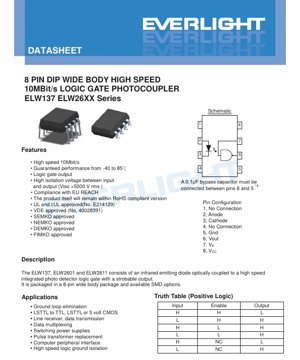
3. Pin Configuration and Functional Description
The device uses an 8-pin DIP configuration. Pins 1 and 4 are No Connection (NC). The input side consists of Pin 2 (Anode) and Pin 3 (Cathode) for the LED. The output side includes Pin 5 (Ground), Pin 6 (VOUT - Output), Pin 7 (VE - Enable), and Pin 8 (VCC - Supply Voltage). The enable pin (VE) controls the output. The truth table shows the logic: when Enable is High, the output is the inverse of the input (active-low). When Enable is Low, the output is forced High regardless of the input. The datasheet mandates a 0.1µF bypass capacitor between pins 8 (VCC) and 5 (GND) for stable operation.
4. Application Suggestions
4.1 Typical Application Scenarios
- Ground Loop Elimination & Logic Level Isolation: Isolating digital signals between subsystems with different ground potentials to prevent noise and ground loops.
- Data Transmission & Line Receivers: Used in serial communication links (RS-232, RS-485 interfaces) for isolation.
- Switching Power Supplies: Providing feedback isolation in flyback or other isolated converter topologies.
- Computer Peripheral Interfaces: Isolating signals to/from printers, industrial I/O cards.
- Pulse Transformer Replacement: Offering a solid-state alternative for signal isolation with simpler drive circuitry.
4.2 Design Considerations
- Input Current Setting: The input LED current must be set using a series resistor. For guaranteed switching, IF should be set above the maximum IFT (5mA). The typical test condition uses 7.5mA. The resistor value is (VDRIVE - VF) / IF.
- Enable Pin Usage: The enable pin can be used for gating output or connecting to a fixed voltage if not needed. It must not exceed VCC by more than 0.5V.
- Output Load: The output can sink up to 13mA for a valid VOL. For driving higher currents or capacitive loads, an external buffer may be required.
- Noise Immunity: For high-noise environments, choose the ELW2611 variant for its superior Common Mode Transient Immunity (CMTI). The recommended drive circuit in Fig. 15 for ELW2611 uses a transistor to sharpen the input LED current edges, further improving CMTI performance.
- Bypassing: The 0.1µF capacitor on the output side is essential to minimize supply noise and ensure stable high-speed operation.
5. Technical Comparison and Selection Guidance
The series includes three main variants: ELW137, ELW2601, and ELW2611. The primary differentiating factor is the Common Mode Transient Immunity (CMTI). The ELW137 has basic isolation. The ELW2601 offers medium CMTI (5,000 V/µs). The ELW2611 provides high CMTI (10,000 - 20,000 V/µs). Selection should be based on the electrical noise environment of the application. For motor drives, industrial PLCs, or noisy power supplies, the ELW2611 is recommended. For less demanding digital isolation, the ELW2601 or ELW137 may be sufficient.
6. Frequently Asked Questions (Based on Technical Parameters)
6.1 What is the maximum data rate achievable?
While the device is specified for 10 Mbit/s, the actual maximum usable rate depends on the propagation delays and rise/fall times. With a maximum propagation delay of 100 ns, the theoretical maximum frequency for a square wave is lower. For reliable data transmission, consider the total pulse distortion and system timing margins.
6.2 How do I calculate the input resistor value?
Use the formula: RIN = (VDRIVE - VF) / IF. Assume VF is the maximum value (1.8V) for worst-case design. For a 5V drive and IF = 10mA, RIN = (5V - 1.8V) / 0.01A = 320 Ohms. Use the nearest standard value (e.g., 330 Ohms).
6.3 Can I use it with 3.3V logic?
The output side VCC can be powered by 3.3V. However, the electrical characteristics are tested with VCC=5.5V. Parameters like VOL, IOH, and propagation delays may differ at 3.3V. The input side is independent; the LED can be driven by a 3.3V source as long as the correct IF is achieved.
6.4 What is the purpose of the Enable pin?
The Enable pin (VE) provides a third-state control. When driven low (<0.8V), it forces the output high, effectively disabling the signal path from input to output. This can be used for multiplexing multiple isolator outputs onto a single bus line or for power-saving modes.
7. Practical Design Case
Scenario: Isolating a 1 Mbit/s UART signal between a 3.3V microcontroller and a 5V RS-485 transceiver in an industrial sensor node.
Design Steps:
- Variant Selection: Choose ELW2611 for high noise immunity in the industrial setting.
- Input Circuit: Microcontroller GPIO (3.3V) drives the LED. Calculate resistor: RIN = (3.3V - 1.8V) / 0.01A = 150 Ohms. Use 150Ω resistor in series with LED anode (Pin 2). Cathode (Pin 3) to microcontroller GND.
- Output Circuit: Power output side with 5V (VCC Pin 8). Connect 0.1µF ceramic capacitor between Pin 8 and Pin 5 (GND). Connect output Pin 6 directly to the RS-485 transceiver's input pin. The transceiver's input impedance acts as the load. Enable Pin 7 can be tied to VCC (5V) via a 10kΩ resistor for always-active operation, or driven by another GPIO for control.
- Layout: Keep the input and output traces physically separated. Place the bypass capacitor as close as possible to pins 8 and 5.
8. Principle of Operation
A photocoupler operates on the principle of optical coupling. An electrical input signal drives an infrared Light Emitting Diode (LED). The light emitted is detected by a photodiode or phototransistor on the isolated output side. In this logic gate photocoupler, the output side contains a more complex integrated circuit. The photodetector's current is amplified and processed by a digital logic gate (typically a Schmitt trigger) to produce a clean, well-defined digital output signal. The optical path provides the electrical isolation barrier, as light can cross a physical gap (through transparent insulation material) where electricity cannot, blocking ground loops and high-voltage transients.
9. Industry Trends
The trend in signal isolation is towards higher speeds, lower power consumption, smaller packages, and integrated functionality. While traditional photocouplers like this DIP package remain widely used, newer technologies are gaining traction. Digital isolators based on CMOS technology with capacitive or magnetic coupling offer significantly higher data rates (up to hundreds of Mbit/s), lower propagation delays, better timing symmetry, and higher reliability over temperature and time. They also integrate multiple channels in tiny packages. However, photocouplers still hold advantages in certain areas like very high isolation voltage capability, simplicity, and cost-effectiveness for many standard-speed applications. The development of high-speed, high-CMTI photocouplers (as seen in the ELW2611) is a response to the need for robust isolation in noisy power electronics and motor drive environments.
LED Specification Terminology
Complete explanation of LED technical terms
Photoelectric Performance
| Term | Unit/Representation | Simple Explanation | Why Important |
|---|---|---|---|
| Luminous Efficacy | lm/W (lumens per watt) | Light output per watt of electricity, higher means more energy efficient. | Directly determines energy efficiency grade and electricity cost. |
| Luminous Flux | lm (lumens) | Total light emitted by source, commonly called "brightness". | Determines if the light is bright enough. |
| Viewing Angle | ° (degrees), e.g., 120° | Angle where light intensity drops to half, determines beam width. | Affects illumination range and uniformity. |
| CCT (Color Temperature) | K (Kelvin), e.g., 2700K/6500K | Warmth/coolness of light, lower values yellowish/warm, higher whitish/cool. | Determines lighting atmosphere and suitable scenarios. |
| CRI / Ra | Unitless, 0–100 | Ability to render object colors accurately, Ra≥80 is good. | Affects color authenticity, used in high-demand places like malls, museums. |
| SDCM | MacAdam ellipse steps, e.g., "5-step" | Color consistency metric, smaller steps mean more consistent color. | Ensures uniform color across same batch of LEDs. |
| Dominant Wavelength | nm (nanometers), e.g., 620nm (red) | Wavelength corresponding to color of colored LEDs. | Determines hue of red, yellow, green monochrome LEDs. |
| Spectral Distribution | Wavelength vs intensity curve | Shows intensity distribution across wavelengths. | Affects color rendering and quality. |
Electrical Parameters
| Term | Symbol | Simple Explanation | Design Considerations |
|---|---|---|---|
| Forward Voltage | Vf | Minimum voltage to turn on LED, like "starting threshold". | Driver voltage must be ≥Vf, voltages add up for series LEDs. |
| Forward Current | If | Current value for normal LED operation. | Usually constant current drive, current determines brightness & lifespan. |
| Max Pulse Current | Ifp | Peak current tolerable for short periods, used for dimming or flashing. | Pulse width & duty cycle must be strictly controlled to avoid damage. |
| Reverse Voltage | Vr | Max reverse voltage LED can withstand, beyond may cause breakdown. | Circuit must prevent reverse connection or voltage spikes. |
| Thermal Resistance | Rth (°C/W) | Resistance to heat transfer from chip to solder, lower is better. | High thermal resistance requires stronger heat dissipation. |
| ESD Immunity | V (HBM), e.g., 1000V | Ability to withstand electrostatic discharge, higher means less vulnerable. | Anti-static measures needed in production, especially for sensitive LEDs. |
Thermal Management & Reliability
| Term | Key Metric | Simple Explanation | Impact |
|---|---|---|---|
| Junction Temperature | Tj (°C) | Actual operating temperature inside LED chip. | Every 10°C reduction may double lifespan; too high causes light decay, color shift. |
| Lumen Depreciation | L70 / L80 (hours) | Time for brightness to drop to 70% or 80% of initial. | Directly defines LED "service life". |
| Lumen Maintenance | % (e.g., 70%) | Percentage of brightness retained after time. | Indicates brightness retention over long-term use. |
| Color Shift | Δu′v′ or MacAdam ellipse | Degree of color change during use. | Affects color consistency in lighting scenes. |
| Thermal Aging | Material degradation | Deterioration due to long-term high temperature. | May cause brightness drop, color change, or open-circuit failure. |
Packaging & Materials
| Term | Common Types | Simple Explanation | Features & Applications |
|---|---|---|---|
| Package Type | EMC, PPA, Ceramic | Housing material protecting chip, providing optical/thermal interface. | EMC: good heat resistance, low cost; Ceramic: better heat dissipation, longer life. |
| Chip Structure | Front, Flip Chip | Chip electrode arrangement. | Flip chip: better heat dissipation, higher efficacy, for high-power. |
| Phosphor Coating | YAG, Silicate, Nitride | Covers blue chip, converts some to yellow/red, mixes to white. | Different phosphors affect efficacy, CCT, and CRI. |
| Lens/Optics | Flat, Microlens, TIR | Optical structure on surface controlling light distribution. | Determines viewing angle and light distribution curve. |
Quality Control & Binning
| Term | Binning Content | Simple Explanation | Purpose |
|---|---|---|---|
| Luminous Flux Bin | Code e.g., 2G, 2H | Grouped by brightness, each group has min/max lumen values. | Ensures uniform brightness in same batch. |
| Voltage Bin | Code e.g., 6W, 6X | Grouped by forward voltage range. | Facilitates driver matching, improves system efficiency. |
| Color Bin | 5-step MacAdam ellipse | Grouped by color coordinates, ensuring tight range. | Guarantees color consistency, avoids uneven color within fixture. |
| CCT Bin | 2700K, 3000K etc. | Grouped by CCT, each has corresponding coordinate range. | Meets different scene CCT requirements. |
Testing & Certification
| Term | Standard/Test | Simple Explanation | Significance |
|---|---|---|---|
| LM-80 | Lumen maintenance test | Long-term lighting at constant temperature, recording brightness decay. | Used to estimate LED life (with TM-21). |
| TM-21 | Life estimation standard | Estimates life under actual conditions based on LM-80 data. | Provides scientific life prediction. |
| IESNA | Illuminating Engineering Society | Covers optical, electrical, thermal test methods. | Industry-recognized test basis. |
| RoHS / REACH | Environmental certification | Ensures no harmful substances (lead, mercury). | Market access requirement internationally. |
| ENERGY STAR / DLC | Energy efficiency certification | Energy efficiency and performance certification for lighting. | Used in government procurement, subsidy programs, enhances competitiveness. |