1. Product Overview
The ELS611-G series represents a family of high-speed, logic gate output photocouplers (opto-isolators) designed for digital signal isolation. These devices integrate an infrared emitting diode optically coupled to a high-speed integrated photodetector with a storable logic gate output. Housed in a compact 6-pin Small Dual In-line Package (SDIP), they are engineered to replace pulse transformers and provide robust ground loop elimination in noisy electrical environments.
The core function is to provide electrical isolation between input and output circuits, preventing ground loops, voltage spikes, and noise from propagating. The logic gate output ensures clean digital signal transmission, making it suitable for interfacing between different logic families or voltage domains.
1.1 Core Advantages and Target Market
The primary advantages of the ELS611-G series include its high-speed capability of up to 10MBit/s, which supports fast digital communication protocols. It offers a high isolation voltage of 5000Vrms, providing excellent protection for sensitive circuits. The devices are compliant with halogen-free requirements (Br <900ppm, Cl <900ppm, Br+Cl <1500ppm), are lead-free, and meet RoHS and EU REACH directives. They carry approvals from major international safety agencies including UL, cUL, VDE, NEMKO, FIMKO, SEMKO, DEMKO, and CQC, facilitating their use in global markets.
The target applications are primarily in industrial automation, power supply systems (e.g., switching power supplies for feedback isolation), computer peripheral interfaces, data transmission systems, data multiplexing, and any scenario requiring reliable, high-speed galvanic isolation for digital signals.
2. In-Depth Technical Parameter Analysis
The following sections provide a detailed, objective analysis of the key electrical and performance parameters specified in the datasheet.
2.1 Absolute Maximum Ratings
These ratings define the stress limits beyond which permanent damage to the device may occur. Operating the device continuously at or near these limits is not recommended.
- Input Forward Current (IF): 20 mA. The maximum continuous current allowed through the input LED.
- Input Reverse Voltage (VR): 5 V. The maximum reverse-bias voltage the input LED can withstand.
- Input Power Dissipation (PD): 40 mW. The maximum power the input side can dissipate.
- Output Supply Voltage (VCC): 7.0 V. The absolute maximum voltage that can be applied to the output side supply pin.
- Output Voltage (VO): 7.0 V. The maximum voltage that can appear at the output pin.
- Output Current (IO): 50 mA. The maximum current the output pin can sink or source.
- Isolation Voltage (VISO): 5000 Vrms for 1 minute. This is a critical safety rating, tested with input pins (1,2,3,4) shorted together and output pins (5,6) shorted together.
- Operating Temperature (TOPR): -40°C to +85°C. The ambient temperature range for normal operation.
- Soldering Temperature (TSOL): 260°C for 10 seconds. This defines the reflow soldering profile tolerance.
2.2 Electrical Characteristics
These are the guaranteed performance parameters under specified test conditions.
2.2.1 Input Characteristics (LED Side)
- Forward Voltage (VF): Typically 1.45V, maximum 1.8V at IF=10mA. This is used to design the input current-limiting circuit.
- Reverse Current (IR): Maximum 10 µA at VR=5V. This indicates the LED's leakage current in the off state.
- Input Capacitance (CIN): Typically 60pF. This parameter affects high-frequency switching performance on the input side.
2.2.2 Output Characteristics
- Supply Current, High Level (ICCH): 7mA to 13mA when IF=0mA (LED off) and VCC=5.5V. This is the quiescent current when the output is in a logic high state.
- Supply Current, Low Level (ICCL): 9mA to 15mA when IF=10mA (LED on) and VCC=5.5V. This is the operating current when the output is actively pulled low.
- Low Level Output Voltage (VOL): Typically 0.4V, maximum 0.6V under the condition VCC=5.5V, IF=5mA, IOL=13mA. This defines the output voltage when sinking current in the low state.
- Input Threshold Current (IFT): Maximum 5mA. This is the minimum input LED current required to guarantee the output switches to a valid low logic level (VOL <= 0.6V) under the specified VCC and IOL conditions. It is a key parameter for determining the required drive current.
2.3 Switching Characteristics
These parameters define the timing performance of the photocoupler, crucial for high-speed data transmission. Test conditions are VCC=5V, IF=7.5mA, CL=15pF, RL=350Ω unless noted.
- Propagation Delay to High Level (tPHL): Typically 40ns, maximum 100ns. Time from input LED turn-off to output rising to a logic high.
- Propagation Delay to Low Level (tPLH): Typically 50ns, maximum 100ns. Time from input LED turn-on to output falling to a logic low.
- Pulse Width Distortion (|tPHL – tPLH|): Typically 10ns, maximum 50ns. The difference between the two propagation delays. A lower value is better for preserving signal integrity and duty cycle.
- Output Rise Time (tr): Typically 50ns. Time for output to rise from 10% to 90% of its final high value.
- Output Fall Time (tf): Typically 10ns. Time for output to fall from 90% to 10% of its initial high value.
- Common Mode Transient Immunity (CMH, CML): Minimum 5 kV/µs. This measures the device's immunity to fast voltage transients between the input and output grounds. CMH applies when the output is high, and CML applies when the output is low. A high value indicates strong rejection of noise coupled through the isolation barrier.
3. Performance Curve Analysis
The datasheet references typical electro-optical characteristic curves. While the specific graphs are not detailed in the provided text, they typically include the following, which are essential for design:
- Current Transfer Ratio (CTR) vs. Forward Current: Shows the efficiency of the optocoupler. For a logic gate type, this is embedded in the switching parameters but can indicate performance over temperature and current.
- Propagation Delay vs. Forward Current: Illustrates how switching speed varies with the LED drive current. Higher IF generally decreases propagation delay but increases power dissipation.
- Propagation Delay vs. Temperature: Shows the timing parameter variation across the operating temperature range.
- Supply Current vs. Temperature: Indicates how power consumption on the output side changes with temperature.
Designers should consult the full datasheet graphs to understand performance boundaries and derating needs for their specific application conditions.
4. Mechanical and Package Information
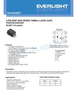
4.1 Pin Configuration and Function
The device uses a 6-pin SDIP package. The pinout is as follows:
- Pin 1: Anode of the input LED.
- Pin 2: No Connection (N.C.).
- Pin 3: Cathode of the input LED.
- Pin 4: Ground (GND) for the output side.
- Pin 5: Output (VOUT). This is the open-collector or totem-pole output of the internal logic gate.
- Pin 6: Supply Voltage (VCC) for the output side.
Critical Design Note: A 0.1µF (or larger) bypass capacitor with good high-frequency characteristics must be connected between pins 6 (VCC) and 4 (GND), placed as close as possible to the package. This is essential for stable operation and achieving the specified switching performance.
4.2 Package Dimensions and PCB Layout
The datasheet provides detailed mechanical drawings for the \"P\" type (surface mount lead form) package. Key dimensions include the overall package body size, lead pitch, and standoff height. A recommended pad layout for surface-mount assembly is also provided to ensure reliable soldering and mechanical strength. Designers must adhere to these layout guidelines to prevent tombstoning or poor solder joints.
5. Soldering and Assembly Guidelines
The absolute maximum rating for soldering temperature is 260°C for 10 seconds. This aligns with typical lead-free reflow soldering profiles. The following precautions should be observed:
- Follow the recommended reflow profile for the specific solder paste used, ensuring the peak temperature and time above liquidus do not exceed the device's rating.
- Avoid excessive mechanical stress on the package during handling.
- Adhere to the recommended PCB pad design to prevent solder bridging or insufficient fillets.
- Storage conditions should be within the specified storage temperature range of -55°C to +125°C, and in a dry environment as per standard moisture sensitivity level (MSL) requirements for surface-mount devices (the specific MSL is not stated in the excerpt).
6. Packaging and Ordering Information
6.1 Model Numbering Rule
The part number follows the format: ELS611X(Y)-VG
- EL: Manufacturer prefix.
- S611: Base part number.
- X: Lead type. \"P\" denotes surface mount lead form.
- (Y): Tape and reel option. \"TA\" or \"TB\" specify different reel packaging styles.
- V: Optional, denotes VDE approval.
- G: Denotes halogen-free construction.
Example: ELS611P(TA)-VG is a surface mount device on TA tape and reel, VDE approved, halogen-free.
6.2 Packing Specifications
The device is available in tape and reel packaging for automated assembly. Both TA and TB options contain 1000 units per reel. The datasheet includes diagrams specifying the tape dimensions, pocket spacing, and reel size.
6.3 Device Marking
The package is marked with a code indicating manufacturing origin, device number, and date code. The format includes: Factory code (\"T\" for Taiwan), \"EL\" for the manufacturer, \"S611\" for the device, a 1-digit year code, a 2-digit week code, and the optional \"V\" for VDE.
7. Application Suggestions and Design Considerations
7.1 Typical Application Circuits
The primary application is digital signal isolation. A typical circuit involves:
- Input Side: A current-limiting resistor in series with the LED (pins 1 and 3) to set the forward current IF. The value is calculated based on the driving voltage and the desired IF (typically between the threshold current IFT and the maximum rating). For high-speed operation, a fast driver is recommended.
- Output Side: VCC (pin 6) is connected to the desired logic supply voltage (up to 7V). Pin 4 (GND) is connected to the output ground. The output pin 5 is connected to the receiving logic input. An external pull-up resistor to VCC may be required depending on the internal output structure (the datasheet schematic shows an active pull-down, suggesting a totem-pole output, but design should verify if pull-up is needed). The critical 0.1µF bypass capacitor between VCC and GND is mandatory.
7.2 Design Considerations
- Speed vs. Current: Higher IF improves propagation delay but increases power dissipation and may reduce long-term reliability. Optimize IF based on required speed and thermal constraints.
- Noise Immunity: The high common-mode transient immunity (5kV/µs) makes it suitable for noisy environments like motor drives and power supplies. Ensure proper PCB layout to minimize parasitic coupling around the isolation barrier.
- Load Considerations: Respect the maximum output current (IO) and voltage (VO) ratings. The output is designed to drive standard logic inputs (TTL, CMOS) and not heavy loads.
- Power Supply Bypassing: Neglecting the recommended bypass capacitor can lead to oscillations, false triggering, and degraded switching performance.
8. Technical Comparison and Differentiation
Compared to standard transistor-output photocouplers, the ELS611-G's integrated logic gate provides several key advantages:
- Higher Speed: 10MBit/s data rate and sub-100ns propagation delays are significantly faster than typical transistor couplers (often in the µs range).
- Clean Digital Output: The logic gate output provides sharp edges and well-defined logic levels without the need for external Schmitt triggers, simplifying circuit design.
- Lower Pulse Distortion: The specified pulse width distortion is low, which is critical for preserving signal integrity in clock and data lines.
- Integrated Functionality: Combines the photodetector, amplifier, and logic gate in one chip, reducing external component count.
9. Frequently Asked Questions (Based on Technical Parameters)
- Q: What is the minimum input current required to guarantee the output switches low?
A: The parameter IFT (Input Threshold Current) has a maximum value of 5mA under the test conditions (VCC=5.5V, VO=0.6V, IOL=13mA). To ensure reliable switching under all conditions, the design should use an IF greater than this value, typically 7.5mA to 10mA as indicated in the switching characteristics. - Q: Can I use this with a 3.3V logic supply on the output?
A: Yes, the device can operate with VCC as low as the minimum required for the internal logic gate to function (not explicitly stated, but typically ~2.7V to 3V for CMOS). The output logic levels will be relative to this VCC. The maximum VCC is 7.0V. - Q: How critical is the 0.1µF bypass capacitor?
A: It is absolutely critical for stable, high-speed operation. It provides a local charge reservoir for the output stage's switching currents, preventing supply rail droop and oscillations that can cause malfunctions. - Q: What does \"storable output\" mean?
A: It likely refers to a latch or flip-flop function that can hold the output state. However, the truth table in the PDF shows a simple inverter function (Input H -> Output L, Input L -> Output H). The term may indicate the output can maintain its state during brief interruptions or has good noise immunity. The schematic should be consulted for clarification.
10. Practical Application Example
Scenario: Isolating a UART Signal in an Industrial Controller.
An industrial microcontroller communicates with a peripheral over UART at 115200 baud. The peripheral operates on a separate power supply with a different ground potential, creating a risk of ground loops.
Implementation:
Two ELS611-G devices are used, one for the TX line (controller to peripheral) and one for the RX line (peripheral to controller). On the TX isolator, the microcontroller's TX pin drives the LED via a current-limiting resistor set for IF=10mA. The isolator's output pin connects to the peripheral's RX input. The isolator's VCC is supplied from the peripheral's 5V or 3.3V rail, with the mandatory bypass capacitor. The process is mirrored for the RX line. This setup breaks the ground connection, prevents noise coupling, and protects the microcontroller from voltage transients on the peripheral side, all while maintaining the integrity of the high-speed serial data.
11. Operating Principle
A photocoupler operates on the principle of optical coupling to achieve electrical isolation. In the ELS611-G:
- An electrical signal applied to the input side causes the infrared Light Emitting Diode (LED) to emit light proportional to the current.
- This light travels across a transparent isolation barrier (typically a mold compound) within the package.
- On the output side, a silicon photodiode or phototransistor detects the light and converts it back into an electrical current.
- This small photocurrent is amplified and processed by a high-speed integrated circuit which includes a logic gate (in this case, likely an inverter or buffer). The IC provides a clean, digital output signal that replicates the input state but is electrically isolated from it.
- The isolation barrier provides high dielectric strength (5000Vrms), preventing current flow and voltage differences between the two sides.
12. Technology Trends
The evolution of photocouplers like the ELS611-G is driven by several key trends in electronics:
- Increased Data Rates: Demand for higher-speed isolation in industrial communications (Profibus, EtherCAT), automotive networks, and renewable energy systems pushes for devices with lower propagation delay and higher common-mode immunity.
- Miniaturization: There is a continuous trend towards smaller packages (e.g., SOIC-4, LSSOP) with the same or better isolation ratings to save PCB space.
- Enhanced Integration: Future devices may integrate more functions, such as power isolation (isolated DC-DC converters) with data isolation in a single package, or multi-channel isolators.
- Material and Process Innovation: Developments in LED efficiency, detector sensitivity, and mold compound purity contribute to lower power consumption, higher speed, and improved long-term reliability.
- Alternative Isolation Technologies: While optocouplers are mature, technologies like capacitive isolation (using SiO2 barriers) and magnetic (GMR) isolation compete in some high-speed, high-density applications. Each technology has its own trade-offs in terms of speed, immunity, power consumption, and cost.
LED Specification Terminology
Complete explanation of LED technical terms
Photoelectric Performance
| Term | Unit/Representation | Simple Explanation | Why Important |
|---|---|---|---|
| Luminous Efficacy | lm/W (lumens per watt) | Light output per watt of electricity, higher means more energy efficient. | Directly determines energy efficiency grade and electricity cost. |
| Luminous Flux | lm (lumens) | Total light emitted by source, commonly called "brightness". | Determines if the light is bright enough. |
| Viewing Angle | ° (degrees), e.g., 120° | Angle where light intensity drops to half, determines beam width. | Affects illumination range and uniformity. |
| CCT (Color Temperature) | K (Kelvin), e.g., 2700K/6500K | Warmth/coolness of light, lower values yellowish/warm, higher whitish/cool. | Determines lighting atmosphere and suitable scenarios. |
| CRI / Ra | Unitless, 0–100 | Ability to render object colors accurately, Ra≥80 is good. | Affects color authenticity, used in high-demand places like malls, museums. |
| SDCM | MacAdam ellipse steps, e.g., "5-step" | Color consistency metric, smaller steps mean more consistent color. | Ensures uniform color across same batch of LEDs. |
| Dominant Wavelength | nm (nanometers), e.g., 620nm (red) | Wavelength corresponding to color of colored LEDs. | Determines hue of red, yellow, green monochrome LEDs. |
| Spectral Distribution | Wavelength vs intensity curve | Shows intensity distribution across wavelengths. | Affects color rendering and quality. |
Electrical Parameters
| Term | Symbol | Simple Explanation | Design Considerations |
|---|---|---|---|
| Forward Voltage | Vf | Minimum voltage to turn on LED, like "starting threshold". | Driver voltage must be ≥Vf, voltages add up for series LEDs. |
| Forward Current | If | Current value for normal LED operation. | Usually constant current drive, current determines brightness & lifespan. |
| Max Pulse Current | Ifp | Peak current tolerable for short periods, used for dimming or flashing. | Pulse width & duty cycle must be strictly controlled to avoid damage. |
| Reverse Voltage | Vr | Max reverse voltage LED can withstand, beyond may cause breakdown. | Circuit must prevent reverse connection or voltage spikes. |
| Thermal Resistance | Rth (°C/W) | Resistance to heat transfer from chip to solder, lower is better. | High thermal resistance requires stronger heat dissipation. |
| ESD Immunity | V (HBM), e.g., 1000V | Ability to withstand electrostatic discharge, higher means less vulnerable. | Anti-static measures needed in production, especially for sensitive LEDs. |
Thermal Management & Reliability
| Term | Key Metric | Simple Explanation | Impact |
|---|---|---|---|
| Junction Temperature | Tj (°C) | Actual operating temperature inside LED chip. | Every 10°C reduction may double lifespan; too high causes light decay, color shift. |
| Lumen Depreciation | L70 / L80 (hours) | Time for brightness to drop to 70% or 80% of initial. | Directly defines LED "service life". |
| Lumen Maintenance | % (e.g., 70%) | Percentage of brightness retained after time. | Indicates brightness retention over long-term use. |
| Color Shift | Δu′v′ or MacAdam ellipse | Degree of color change during use. | Affects color consistency in lighting scenes. |
| Thermal Aging | Material degradation | Deterioration due to long-term high temperature. | May cause brightness drop, color change, or open-circuit failure. |
Packaging & Materials
| Term | Common Types | Simple Explanation | Features & Applications |
|---|---|---|---|
| Package Type | EMC, PPA, Ceramic | Housing material protecting chip, providing optical/thermal interface. | EMC: good heat resistance, low cost; Ceramic: better heat dissipation, longer life. |
| Chip Structure | Front, Flip Chip | Chip electrode arrangement. | Flip chip: better heat dissipation, higher efficacy, for high-power. |
| Phosphor Coating | YAG, Silicate, Nitride | Covers blue chip, converts some to yellow/red, mixes to white. | Different phosphors affect efficacy, CCT, and CRI. |
| Lens/Optics | Flat, Microlens, TIR | Optical structure on surface controlling light distribution. | Determines viewing angle and light distribution curve. |
Quality Control & Binning
| Term | Binning Content | Simple Explanation | Purpose |
|---|---|---|---|
| Luminous Flux Bin | Code e.g., 2G, 2H | Grouped by brightness, each group has min/max lumen values. | Ensures uniform brightness in same batch. |
| Voltage Bin | Code e.g., 6W, 6X | Grouped by forward voltage range. | Facilitates driver matching, improves system efficiency. |
| Color Bin | 5-step MacAdam ellipse | Grouped by color coordinates, ensuring tight range. | Guarantees color consistency, avoids uneven color within fixture. |
| CCT Bin | 2700K, 3000K etc. | Grouped by CCT, each has corresponding coordinate range. | Meets different scene CCT requirements. |
Testing & Certification
| Term | Standard/Test | Simple Explanation | Significance |
|---|---|---|---|
| LM-80 | Lumen maintenance test | Long-term lighting at constant temperature, recording brightness decay. | Used to estimate LED life (with TM-21). |
| TM-21 | Life estimation standard | Estimates life under actual conditions based on LM-80 data. | Provides scientific life prediction. |
| IESNA | Illuminating Engineering Society | Covers optical, electrical, thermal test methods. | Industry-recognized test basis. |
| RoHS / REACH | Environmental certification | Ensures no harmful substances (lead, mercury). | Market access requirement internationally. |
| ENERGY STAR / DLC | Energy efficiency certification | Energy efficiency and performance certification for lighting. | Used in government procurement, subsidy programs, enhances competitiveness. |