Table of Contents
- 1. Product Overview
- 1.1 Core Advantages and Target Market
- 2. Technical Parameter Deep-Dive
- 2.1 Absolute Maximum Ratings
- 2.2 Electrical Characteristics: Input & Output
- 2.3 Transfer Characteristics
- 2.4 Switching Characteristics
- 3. Device Variants and Truth Tables
- 3.1 EL2200 (Three-State Output)
- 3.2 EL2201/EL2202 (Standard Output)
- 4. Application Suggestions and Design Considerations
- 4.1 Typical Application Circuits
- 4.2 Critical Design Considerations
- 5. Mechanical, Packaging, and Assembly
- 5.1 Package Information
- 5.2 Soldering and Handling
- 6. Technical Comparison and FAQs
- 6.1 Differentiation from Other Photocouplers
- 6.2 Frequently Asked Questions (Based on Parameters)
- 7. Operational Principle and Trends
- 7.1 Basic Operating Principle
- 7.2 Industry Trends
- LED Specification Terminology
- Photoelectric Performance
- Electrical Parameters
- Thermal Management & Reliability
- Packaging & Materials
- Quality Control & Binning
- Testing & Certification
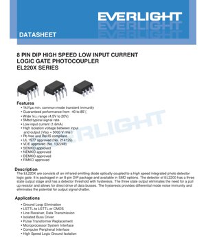
1. Product Overview
The EL220X series represents a family of high-performance, high-speed logic gate photocouplers (opto-isolators) designed for digital signal isolation. The core function is to provide galvanic isolation between input and output circuits while transmitting logic-level signals with high fidelity and speed. The device integrates an infrared emitting diode optically coupled to a high-speed integrated photodetector with a logic gate output stage. It is offered in a standard 8-pin Dual In-line Package (DIP) and is also available in Surface-Mount Device (SMD) variants.
The primary advantage of this series lies in its combination of high speed and low input current requirements. It is engineered to replace pulse transformers and other isolation methods in demanding digital interfaces, offering superior noise immunity, simpler design integration, and reliable performance across a wide temperature range.
1.1 Core Advantages and Target Market
The EL220X photocoupler is distinguished by several key features that define its application space:
- High-Speed Data Transmission: A typical signal rate of 5 Megabaud (Mbd) enables its use in fast digital communication links, microprocessor system interfaces, and computer peripheral interfaces where timing is critical.
- Excellent Noise Immunity: A minimum Common Mode Transient Immunity (CMTI) of 1kV/μs ensures reliable operation in electrically noisy environments, such as industrial controls and motor drives, by rejecting fast voltage transients between the input and output grounds.
- Low Input Drive Requirement: An input threshold current of 1.6mA (max) allows direct interfacing with low-power logic families like LSTTL and CMOS, simplifying driver circuit design and reducing system power consumption.
- Robust Isolation: A high isolation voltage of 5000 Vrms between input and output provides a strong safety barrier and protection for sensitive circuitry, crucial for medical equipment, industrial automation, and power supply feedback loops.
- Wide Operating Range: Guaranteed performance from -40°C to +85°C and a supply voltage (VCC) range of 4.5V to 20V make it suitable for automotive, industrial, and extended commercial temperature applications.
The target markets include industrial automation, programmable logic controllers (PLCs), data acquisition systems, isolated bus drivers, medical instrumentation requiring patient isolation, telecommunications equipment, and any application requiring ground loop elimination or high-voltage isolation for digital signals.
2. Technical Parameter Deep-Dive
The electrical and transfer characteristics of the EL220X series are specified under conditions of TA = -40°C to 85°C, VCC = 4.5V to 20V, and specific input/enable conditions, ensuring reliable operation across the entire stated range.
2.1 Absolute Maximum Ratings
These ratings define the stress limits beyond which permanent damage may occur. They are not for continuous operation.
- Input Forward Current (IF): 50 mA (max). This limits the peak current through the internal LED.
- Input Reverse Voltage (VR): 5 V (max). The LED should not be subjected to reverse bias exceeding this value.
- Output Current (IO): 25 mA (max). The maximum continuous current the output transistor can sink or source.
- Supply/Output Voltage (VCC, VO): 20 V (max). The maximum voltage applied to the output side supply pin or the output pin itself.
- Isolation Voltage (VISO): 5000 Vrms. This is the hi-pot test voltage for one minute, defining the basic insulation capability between input and output.
- Total Power Dissipation (PT): 210 mW. The maximum power the entire package can dissipate at 25°C ambient.
2.2 Electrical Characteristics: Input & Output
Input Characteristics:
- Forward Voltage (VF): Typically 1.4V, with a maximum of 1.8V at IF=10mA. This parameter is essential for designing the current-limiting resistor for the input LED.
- Temperature Coefficient of VF: Approximately -1.8 mV/°C. The LED forward voltage decreases as temperature increases, a common characteristic of diodes.
- Input Capacitance (CIN): Typically 60 pF. This affects the high-frequency response and drive requirements of the input circuit.
Output & Supply Characteristics:
- Supply Currents (ICCH, ICCL): The current drawn by the output-side IC. ICCH (output high) is typically 2.3-3mA, and ICCL (output low) is typically 3.7-4.5mA, depending on VCC. These values are critical for system power budget calculations.
- Output Logic Levels:
- High-Level Output Voltage (VOH): Minimum of 2.4V when sinking -2.6mA (IOH). This guarantees compatibility with TTL and CMOS logic high input thresholds.
- Low-Level Output Voltage (VOL): Maximum of 0.5V when sourcing 6.4mA (IOL) at VCC=4.5V. This ensures a solid logic low state.
- Enable Characteristics (EL2200 only): The three-state enable function has specific voltage (VEH min 2.0V, VEL max 0.8V) and current (IEH, IEL) requirements for proper control of the high-impedance output state.
2.3 Transfer Characteristics
These parameters define the signal transfer behavior from input to output.
- Input Threshold Current (IFT): Maximum of 1.6mA. This is the guaranteed current needed at the input LED to force the output to a valid logic low state under specified conditions. It directly relates to the device's sensitivity.
- Input Current Hysteresis (IHYS): Typically 0.03mA. This built-in hysteresis provides differential mode noise immunity, preventing output chatter when the input signal is near the switching threshold.
- Output Leakage Currents (IOHH, IOZL, IOZH): These are the small currents that flow in the output high state or high-impedance state when the output is off. They are typically in the microamp range but must be considered in high-impedance bus applications.
- Short-Circuit Output Current (IOSL, IOSH): The current the output can deliver into a short circuit, typically 25-40mA. This indicates the output stage's robustness but is not a condition for continuous operation.
2.4 Switching Characteristics
These parameters define the timing performance, crucial for high-speed data transmission.
- Propagation Delays (tPLH, tPHL): The time from the input LED crossing its threshold to the output crossing its logic threshold. Typical values are 100ns (low-to-high) and 105ns (high-to-low), with maximums of 300ns. These delays limit the maximum usable data rate.
- Rise/Fall Times (tr, tf): The output signal edge speeds. Typical tr is 45ns and tf is 10ns. Faster edges improve signal integrity but may increase EMI.
- Enable/Disable Times (EL2200 only): Parameters like tPZH, tPZL, tPHZ, tPLZ define how quickly the output enters or leaves the high-impedance state when the enable pin is toggled. These are critical for bus-sharing applications.
- Common Mode Transient Immunity (CMH, CML): Minimum of 1000 V/μs. This quantifies the device's ability to maintain correct output logic states during fast voltage transients between the input and output grounds. The test is performed with |VCM|=50V.
3. Device Variants and Truth Tables
The EL220X series includes specific variants with different output configurations.
3.1 EL2200 (Three-State Output)
The EL2200 features a three-state (tri-state) output. This allows multiple devices to be connected to a common data bus without contention. The output can be in a logic High, logic Low, or a high-impedance (Z) state. The high-impedance state is controlled by an active-low Enable (E) pin.
Truth Table for EL2200:
| Input (LED) | Enable (E) | Output |
|---|---|---|
| H (ON) | H | Z (High-Impedance) |
| L (OFF) | H | Z (High-Impedance) |
| H (ON) | L | H |
| L (OFF) | L | L |
When Enable is high, the output is disabled (high-Z) regardless of the input. When Enable is low, the output actively follows the input state (non-inverting).
3.2 EL2201/EL2202 (Standard Output)
The EL2201 and EL2202 have a standard, always-active output with no enable pin. The output directly follows the input state. The difference between EL2201 and EL2202 is typically in-channel-to-channel matching or other parametric selections not detailed in this excerpt.
Truth Table for EL2201/02:
| Input (LED) | Output |
|---|---|
| H (ON) | H |
| L (OFF) | L |
The transfer function is non-inverting.
4. Application Suggestions and Design Considerations
4.1 Typical Application Circuits
1. Microprocessor System Interface / Isolated Bus Driver: The EL2200 is ideal for this. Multiple EL2200s can have their outputs connected to a microprocessor data bus. Each device's Enable pin is controlled by an address decoder. Only the selected device drives the bus, while others remain in high-Z state, preventing bus contention.
2. Ground Loop Elimination in Data Transmission: When sending digital signals (e.g., RS-232, RS-485 control signals) between systems with different ground potentials, the EL220X breaks the galvanic connection, preventing ground loop currents that cause noise and errors. Its high CMTI handles the ground shift.
3. Pulse Transformer Replacement: In switch-mode power supply feedback loops or gate drive circuits, the EL220X can replace small pulse transformers. It offers advantages like simpler design (no concern for transformer saturation, simpler driver), better stability over temperature, and potentially lower cost.
4.2 Critical Design Considerations
- Input Current Limiting Resistor (RLIM): This is the most critical external component. It must be calculated based on the forward voltage (VF) of the LED, the drive voltage (VDRIVE), and the desired forward current (IF). IF must be greater than IFT (1.6mA max) for a guaranteed low output but should not exceed the Absolute Maximum Rating.
Formula: RLIM = (VDRIVE - VF) / IF
Example: For VDRIVE=5V, VF=1.4V, and IF=5mA, RLIM = (5 - 1.4) / 0.005 = 720Ω. Use a standard 680Ω or 750Ω resistor. - Power Supply Decoupling: A bypass capacitor (typically 0.1µF ceramic) should be placed as close as possible between the VCC and GND pins on the output side to minimize noise and ensure stable switching.
- Output Loading: Ensure the connected load does not require more sink/source current (IOL/IOH) than specified. For heavy loads, an external buffer may be needed. The sum of ICC and the load current must be considered for the output side power supply.
- Enable Pin Handling (EL2200): The Enable pin must not be left floating. It should be tied to VCC (via a resistor if necessary) to disable the output, or actively driven by control logic.
- PCB Layout for High CMTI: To maintain the high CMTI rating, maximize the creepage and clearance distance on the PCB between the input and output sections. Avoid running input and output traces parallel or close to each other. Use a slot or barrier in the PCB if necessary.
5. Mechanical, Packaging, and Assembly
5.1 Package Information
The device is housed in a standard 8-pin DIP package. The exact body dimensions, lead spacing, and seating plane should be obtained from the detailed mechanical drawing (not fully provided in this excerpt). Key points include:
- Standard DIP pin spacing: 2.54mm (0.1") between pins in a row, and 7.62mm (0.3") between rows.
- The package is available in both through-hole and SMD styles.
- Polarity is indicated by a notch or dot at the end of the package corresponding to pin 1.
5.2 Soldering and Handling
- Soldering Temperature: The absolute maximum soldering temperature is 260°C. This refers to the peak temperature experienced by the package body during reflow or wave soldering processes.
- ESD Precautions: Photocouplers contain sensitive semiconductor junctions. Standard ESD (Electrostatic Discharge) handling procedures should be followed during assembly and handling.
- Storage Conditions: The storage temperature range is -55°C to +125°C. Devices should be stored in a dry, anti-static environment.
6. Technical Comparison and FAQs
6.1 Differentiation from Other Photocouplers
The EL220X series differentiates itself in the photocoupler market through its specific combination of attributes:
- vs. Standard Transistor-Output Optocouplers (e.g., 4N25): The EL220X is significantly faster (5Mbd vs. ~100kbd), has a defined logic output stage (vs. an analog transistor), and features much higher CMTI. It is designed for digital signals, not analog isolation.
- vs. Other High-Speed Logic Gate Optocouplers: Its competitive advantages include the very low 1.6mA input threshold current, which reduces driver burden, and the availability of a three-state version (EL2200) for bus applications, which is not common in all families.
- vs. Digital Isolators (Silicon-based): Digital isolators use capacitive or magnetic coupling and can achieve much higher speeds (e.g., 100Mbps+). However, optocouplers like the EL220X offer superior isolation voltage (5000Vrms vs. typically 2500-5000VRMS for many digital isolators) and have a long-proven reliability record in high-noise, high-voltage environments. The choice depends on the required speed, isolation strength, and cost targets.
6.2 Frequently Asked Questions (Based on Parameters)
Q: What is the maximum data rate I can achieve with this device?
A: The typical signal rate is 5 Megabaud. The maximum practical data rate is limited by the propagation delays and rise/fall times. For a non-return-to-zero (NRZ) signal, a conservative estimate for the maximum frequency is 1/(2 * tPLH). Using the typical tPLH of 100ns, this suggests a maximum frequency around 5 MHz, which aligns with the 5 Mbd rating. For reliable operation, design with the maximum specified delays (300ns).
Q: How do I use the three-state function of the EL2200?
A> Connect the Enable (E) pin to your system's control logic. Drive it high (>\u20092.0V) to place the output in a high-impedance state, effectively disconnecting it from the bus or line. Drive it low (<\u20090.8V) to enable the output, allowing it to actively drive High or Low based on the input LED state. Never leave the pin unconnected.
Q: The datasheet mentions "hysteresis." What does this mean for my design?
A: Input current hysteresis means the current required to turn the output ON (IFT) is slightly higher than the current at which it turns OFF. This creates a noise margin. If your input signal has slow edges or noise superimposed on it, the hysteresis prevents the output from oscillating or chattering as the input passes through the switching threshold, ensuring a clean digital transition.
Q: Can I use this device to isolate analog signals?
A: No, the EL220X is specifically a logic gate photocoupler. Its output is a digital logic level (High/Low/Z), not a linear representation of the input LED current. For analog signal isolation, a linear optocoupler (with a phototransistor or photodiode output operating in its linear region) or an isolation amplifier should be used.
7. Operational Principle and Trends
7.1 Basic Operating Principle
The operation is based on optoelectronic conversion. An electrical current applied to the input side causes an Infrared Emitting Diode (IRED) to emit light. This light traverses an optically transparent isolation barrier within the package. On the output side, a silicon photodetector (typically a photodiode integrated with a signal conditioning IC) converts the received light back into an electrical current. This photocurrent is processed by a high-speed comparator or logic circuit with hysteresis to produce a clean, noise-immune digital output signal that replicates the input logic state. The key is that the signal is transmitted by light, providing the galvanic isolation between the two electrical circuits.
7.2 Industry Trends
Photocoupler technology continues to evolve. Trends relevant to devices like the EL220X include:
- Higher Speed: Demand for faster data isolation in industrial Ethernet, servo drives, and renewable energy systems pushes for photocouplers with rates beyond 10 Mbd and even into the 25-50 Mbd range.
- Lower Power Consumption: Reducing IF and ICC is a constant goal to meet the needs of portable and energy-efficient equipment.
- Enhanced Integration: Combining multiple isolated channels in a single package (dual, quad) or integrating additional functions like fail-safe outputs or I2C isolation is becoming more common.
- Package Miniaturization: The move towards smaller, surface-mount packages like SOIC-8 and even smaller footprints to save board space in compact designs.
- Improved Reliability and Longevity: Focus on extending the operational lifetime, especially the LED's longevity, under high-temperature and continuous operation conditions.
The EL220X series, with its balanced set of speed, low input current, and robust isolation, occupies a well-established position in this evolving landscape, serving applications where its specific performance envelope is optimal.
LED Specification Terminology
Complete explanation of LED technical terms
Photoelectric Performance
| Term | Unit/Representation | Simple Explanation | Why Important |
|---|---|---|---|
| Luminous Efficacy | lm/W (lumens per watt) | Light output per watt of electricity, higher means more energy efficient. | Directly determines energy efficiency grade and electricity cost. |
| Luminous Flux | lm (lumens) | Total light emitted by source, commonly called "brightness". | Determines if the light is bright enough. |
| Viewing Angle | ° (degrees), e.g., 120° | Angle where light intensity drops to half, determines beam width. | Affects illumination range and uniformity. |
| CCT (Color Temperature) | K (Kelvin), e.g., 2700K/6500K | Warmth/coolness of light, lower values yellowish/warm, higher whitish/cool. | Determines lighting atmosphere and suitable scenarios. |
| CRI / Ra | Unitless, 0–100 | Ability to render object colors accurately, Ra≥80 is good. | Affects color authenticity, used in high-demand places like malls, museums. |
| SDCM | MacAdam ellipse steps, e.g., "5-step" | Color consistency metric, smaller steps mean more consistent color. | Ensures uniform color across same batch of LEDs. |
| Dominant Wavelength | nm (nanometers), e.g., 620nm (red) | Wavelength corresponding to color of colored LEDs. | Determines hue of red, yellow, green monochrome LEDs. |
| Spectral Distribution | Wavelength vs intensity curve | Shows intensity distribution across wavelengths. | Affects color rendering and quality. |
Electrical Parameters
| Term | Symbol | Simple Explanation | Design Considerations |
|---|---|---|---|
| Forward Voltage | Vf | Minimum voltage to turn on LED, like "starting threshold". | Driver voltage must be ≥Vf, voltages add up for series LEDs. |
| Forward Current | If | Current value for normal LED operation. | Usually constant current drive, current determines brightness & lifespan. |
| Max Pulse Current | Ifp | Peak current tolerable for short periods, used for dimming or flashing. | Pulse width & duty cycle must be strictly controlled to avoid damage. |
| Reverse Voltage | Vr | Max reverse voltage LED can withstand, beyond may cause breakdown. | Circuit must prevent reverse connection or voltage spikes. |
| Thermal Resistance | Rth (°C/W) | Resistance to heat transfer from chip to solder, lower is better. | High thermal resistance requires stronger heat dissipation. |
| ESD Immunity | V (HBM), e.g., 1000V | Ability to withstand electrostatic discharge, higher means less vulnerable. | Anti-static measures needed in production, especially for sensitive LEDs. |
Thermal Management & Reliability
| Term | Key Metric | Simple Explanation | Impact |
|---|---|---|---|
| Junction Temperature | Tj (°C) | Actual operating temperature inside LED chip. | Every 10°C reduction may double lifespan; too high causes light decay, color shift. |
| Lumen Depreciation | L70 / L80 (hours) | Time for brightness to drop to 70% or 80% of initial. | Directly defines LED "service life". |
| Lumen Maintenance | % (e.g., 70%) | Percentage of brightness retained after time. | Indicates brightness retention over long-term use. |
| Color Shift | Δu′v′ or MacAdam ellipse | Degree of color change during use. | Affects color consistency in lighting scenes. |
| Thermal Aging | Material degradation | Deterioration due to long-term high temperature. | May cause brightness drop, color change, or open-circuit failure. |
Packaging & Materials
| Term | Common Types | Simple Explanation | Features & Applications |
|---|---|---|---|
| Package Type | EMC, PPA, Ceramic | Housing material protecting chip, providing optical/thermal interface. | EMC: good heat resistance, low cost; Ceramic: better heat dissipation, longer life. |
| Chip Structure | Front, Flip Chip | Chip electrode arrangement. | Flip chip: better heat dissipation, higher efficacy, for high-power. |
| Phosphor Coating | YAG, Silicate, Nitride | Covers blue chip, converts some to yellow/red, mixes to white. | Different phosphors affect efficacy, CCT, and CRI. |
| Lens/Optics | Flat, Microlens, TIR | Optical structure on surface controlling light distribution. | Determines viewing angle and light distribution curve. |
Quality Control & Binning
| Term | Binning Content | Simple Explanation | Purpose |
|---|---|---|---|
| Luminous Flux Bin | Code e.g., 2G, 2H | Grouped by brightness, each group has min/max lumen values. | Ensures uniform brightness in same batch. |
| Voltage Bin | Code e.g., 6W, 6X | Grouped by forward voltage range. | Facilitates driver matching, improves system efficiency. |
| Color Bin | 5-step MacAdam ellipse | Grouped by color coordinates, ensuring tight range. | Guarantees color consistency, avoids uneven color within fixture. |
| CCT Bin | 2700K, 3000K etc. | Grouped by CCT, each has corresponding coordinate range. | Meets different scene CCT requirements. |
Testing & Certification
| Term | Standard/Test | Simple Explanation | Significance |
|---|---|---|---|
| LM-80 | Lumen maintenance test | Long-term lighting at constant temperature, recording brightness decay. | Used to estimate LED life (with TM-21). |
| TM-21 | Life estimation standard | Estimates life under actual conditions based on LM-80 data. | Provides scientific life prediction. |
| IESNA | Illuminating Engineering Society | Covers optical, electrical, thermal test methods. | Industry-recognized test basis. |
| RoHS / REACH | Environmental certification | Ensures no harmful substances (lead, mercury). | Market access requirement internationally. |
| ENERGY STAR / DLC | Energy efficiency certification | Energy efficiency and performance certification for lighting. | Used in government procurement, subsidy programs, enhances competitiveness. |