Table of Contents
- 1. Product Overview
- 1.1 Core Advantages and Target Market
- 2. In-Depth Technical Parameter Analysis
- 2.1 Absolute Maximum Ratings
- 2.2 Electrical & Transfer Characteristics
- 2.3 Switching Characteristics
- 3. Pin Configuration and Functional Description
- 4. Application Guidelines and Design Considerations
- 4.1 Typical Application Scenarios
- 4.2 Critical Design Considerations
- 5. Mechanical, Packaging, and Assembly Information
- 5.1 Package Dimensions and Mounting
- 5.2 Soldering and Handling
- 6. Ordering Information and Model Differentiation
- 7. Technical Comparison and FAQs
- 7.1 Comparison with Other Isolator Types
- 7.2 Frequently Asked Questions (Based on Parameters)
- 8. Operational Principle and Technology Trends
- 8.1 Principle of Operation
- 8.2 Industry Trends
1. Product Overview
The EL050L series represents a high-performance, high-speed transistor photocoupler (opto-isolator) designed for applications requiring robust electrical isolation and fast digital signal transmission. The core function of this device is to transfer electrical signals between two isolated circuits using light, thereby preventing ground loops, blocking high voltages, and reducing noise transmission.
At its heart, the device contains an infrared light-emitting diode (LED) that is optically coupled to a high-speed integrated photodetector with a logic gate output. This configuration allows it to function as a digital isolator. It is housed in a compact 8-pin Small Outline Package (SOP), making it suitable for modern surface-mount technology (SMT) assembly processes.
1.1 Core Advantages and Target Market
The EL050L is engineered with several key advantages that define its position in the market:
- High-Speed Operation: Capable of data rates up to 1 Megabit per second (1Mbit/s), it is suitable for digital communication interfaces and fast switching control signals.
- Robust Isolation: It provides a high isolation voltage of 3750 Vrms between its input and output sides, ensuring safety and reliability in high-voltage environments.
- Excellent Noise Immunity: It features a high common-mode transient immunity (CMTI) of 15 kV/μs minimum, allowing it to reject fast voltage transients that appear across the isolation barrier, which is critical in noisy power electronics like motor drives.
- Dual Supply Voltage: The output side is compatible with both 3.3V and 5V logic systems, offering design flexibility.
- Environmental Compliance: The device is halogen-free, Pb-free, and compliant with RoHS, REACH, and various international safety standards (UL, cUL, VDE, etc.).
The primary target markets include industrial automation, power supply feedback circuits, motor drive systems, communication interface isolation, and any application where ground potential differences or high-voltage noise is a concern.
2. In-Depth Technical Parameter Analysis
This section provides a detailed, objective interpretation of the key electrical and optical parameters specified in the datasheet.
2.1 Absolute Maximum Ratings
These ratings define the stress limits beyond which permanent damage to the device may occur. They are not intended for normal operation.
- Input Forward Current (IF): 25 mA continuous. This limits the maximum DC current through the input LED.
- Peak Forward Current (IFP): 50 mA for pulses with a 50% duty cycle and 1ms pulse width. This allows for higher instantaneous drive currents for brief periods.
- Reverse Voltage (VR): 5 V. The input LED must not be subjected to a reverse bias exceeding this value.
- Output Voltage (VO) & Supply Voltage (VCC): -0.5V to +7V. The output pin and the supply pin must remain within this voltage range relative to the output ground (GND).
- Isolation Voltage (VISO): 3750 Vrms for 1 minute. This is the hi-pot test voltage applied between the shorted input pins (1-4) and shorted output pins (5-8) to verify the integrity of the isolation barrier.
- Operating Temperature (TOPR): -40°C to +85°C. The device is guaranteed to meet its electrical specifications within this ambient temperature range.
2.2 Electrical & Transfer Characteristics
These parameters are guaranteed over the operating temperature range of 0°C to 70°C unless otherwise noted.
Input Characteristics:
- Forward Voltage (VF): Typically 1.45V, with a maximum of 1.8V at a forward current (IF) of 16 mA. This is the voltage drop across the LED when conducting.
- Temperature Coefficient of VF: Approximately -1.9 mV/°C. The LED's forward voltage decreases as temperature increases, which is a typical characteristic of semiconductor diodes.
Output Characteristics:
- Logic High Output Current (IOH): Very low leakage current (max 0.5 µA) when the input is off (IF=0). This indicates a good "off" state.
- Supply Currents: ICCL (logic low state, input on) is typically 100 µA, while ICCH (logic high state, input off) is much lower, typically 0.01 µA. These values determine the quiescent power consumption of the output stage.
Transfer Characteristics:
- Current Transfer Ratio (CTR): For the EL050L, the CTR is specified between 7% and 50% under standard test conditions (IF=16mA, VO=0.4V, VCC=3.3V, TA=25°C). CTR is the ratio of the output transistor's collector current to the input LED's forward current. A minimum CTR of 5% is guaranteed under slightly different conditions (VO=0.5V). This parameter is crucial for ensuring the output can sink sufficient current to pull the output voltage low.
- Logic Low Output Voltage (VOL): Typically 0.12V, with a maximum of 0.4V when IF=16mA and the output is sinking 3 mA. This low saturation voltage is essential for clean logic-low signaling.
2.3 Switching Characteristics
These parameters define the dynamic performance of the photocoupler, critical for high-speed applications. Tests are performed at IF=16mA and VCC=3.3V.
- Propagation Delay Times:
- TPHL (to Logic Low): Maximum 2.0 µs with a 4.1kΩ load resistor (RL). Faster switching (max 0.9 µs) is achieved with a smaller 1.9kΩ load. This is the delay from the input LED turning on to the output voltage falling to a logic low level.
- TPLH (to Logic High): Similarly, maximum 2.0 µs (4.1kΩ) and 0.9 µs (1.9kΩ). This is the delay from the input LED turning off to the output voltage rising to a logic high level.
- Common Mode Transient Immunity (CMTI): A key robustness metric. The device is tested to withstand a minimum of 1000 V/μs (typical) of common-mode voltage slew rate (dVCM/dt) while maintaining the correct output logic state, both high and low. The test uses a 10V peak-to-peak common-mode pulse. High CMTI prevents false triggering from noise spikes across the isolation barrier.
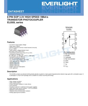
3. Pin Configuration and Functional Description
The device uses an 8-pin SOP package. The pinout is as follows:
- Pin 1, 4: No Connection (NC). These pins are internally unconnected and can be left floating or connected to ground for shielding in the PCB layout.
- Pin 2: Anode of the input infrared LED.
- Pin 3: Cathode of the input infrared LED.
- Pin 5: Ground (GND) for the output side circuitry.
- Pin 6: Output Voltage (VOUT). This is the open-collector output of the photodetector. An external pull-up resistor to VCC is required.
- Pin 7: Strobe or Bias Voltage (VB). Based on the description ("strobable output"), this pin likely provides a means to enable or disable the output stage for noise reduction or multi-device multiplexing. The datasheet does not provide detailed application information for this pin; consulting the manufacturer's application notes is recommended.
- Pin 8: Supply Voltage (VCC) for the output side. Accepts 3.3V or 5V.
4. Application Guidelines and Design Considerations
4.1 Typical Application Scenarios
- Gate Drive Isolation in Motor Drives/Inverters: Isolating the low-voltage microcontroller PWM signals from the high-voltage, noisy gate driver circuits for IGBTs or MOSFETs. The high CMTI is essential here.
- Feedback Loop Isolation in Switched-Mode Power Supplies (SMPS): Providing isolated voltage/current feedback from the secondary (output) side to the primary-side controller, ensuring safety and regulation.
- Communication Interface Isolation: Isolating serial data lines (e.g., RS-485, CAN, UART) to break ground loops and protect sensitive logic from transients.
- Logic Level Translation and Ground Separation: Interfacing between systems with different ground potentials or logic voltage levels (e.g., 3.3V LVTTL to 5V CMOS).
- Replacement for Pulse Transformers or Slower Phototransistor Couplers: Offering a smaller, more integrated, and potentially more reliable solution with comparable or better speed.
4.2 Critical Design Considerations
- Input Current Limiting Resistor: A series resistor must always be used with the input LED to limit the forward current (IF) to a safe value, typically between 5mA and 16mA as per the datasheet's test conditions. The resistor value is calculated as Rlimit = (Vdrive - VF) / IF.
- Output Pull-Up Resistor: The open-collector output on Pin 6 requires an external pull-up resistor to VCC. The value of this resistor (RL) is a critical trade-off:
- Smaller RL (e.g., 1.9kΩ): Provides faster rise times (lower TPLH) and stronger pull-up, but increases power dissipation when the output is low (IOL = VCC/RL). Ensure the output's current sinking capability is not exceeded.
- Larger RL (e.g., 4.1kΩ or 10kΩ): Reduces power consumption but results in slower rise times and may be more susceptible to noise pickup.
- Power Supply Decoupling: Place a 0.1µF ceramic capacitor close to pins 8 (VCC) and 5 (GND) to provide a local, low-impedance source of current for high-speed switching and to filter noise.
- PCB Layout for High CMTI: To maintain the high common-mode transient immunity, minimize the parasitic capacitance across the isolation barrier. This means keeping the input and output traces physically separated on the PCB, avoiding parallel runs, and following the recommended creepage and clearance distances specified in safety standards.
- Strobe Pin (VB) Usage: If the strobable feature is not required, this pin should be connected according to the manufacturer's recommendation, which is often to VCC or left floating. The datasheet lacks explicit guidance, so verification is needed.
5. Mechanical, Packaging, and Assembly Information
5.1 Package Dimensions and Mounting
The device is housed in an 8-pin SOP (Small Outline Package). The datasheet includes a package drawing with critical dimensions (length, width, height, lead pitch, etc.). Designers must adhere to these dimensions for PCB footprint creation.
A recommended pad layout for surface mounting is typically provided to ensure reliable solder joint formation during reflow soldering. This layout accounts for thermal relief and proper solder fillets.
5.2 Soldering and Handling
- Reflow Soldering: The device can withstand a maximum soldering temperature (TSOL) of 260°C for 10 seconds. Standard lead-free reflow profiles (IPC/JEDEC J-STD-020) are generally applicable.
- Moisture Sensitivity: SOP packages are typically moisture-sensitive. If the device is supplied in a dry pack, it must be baked according to the manufacturer's instructions if the exposure time limit is exceeded before soldering.
- Storage Conditions: The absolute maximum storage temperature range is -40°C to +125°C. Store in a dry, anti-static environment.
6. Ordering Information and Model Differentiation
The part number follows the format: EL050L(Z)-V
- EL050L: Base part number for the series.
- (Z): Tape and Reel option.
- None: Packed in tubes of 100 units.
- (TA): TA type tape and reel, 2000 units per reel.
- (TB): TB type tape and reel, 2000 units per reel.
- -V: Optional suffix indicating the device is certified to VDE standards. If omitted, the device has standard approvals (UL, cUL, etc.).
Examples:
- EL050L: Standard part in tube.
- EL050L-V: VDE-certified part in tube.
- EL050L(TA)-V: VDE-certified part on TA-type tape and reel.
7. Technical Comparison and FAQs
7.1 Comparison with Other Isolator Types
- vs. Traditional Phototransistor Couplers: The EL050L is significantly faster (1Mbit/s vs. often <100kbit/s) due to its integrated logic-gate output stage, which actively drives the output rather than relying on a passive phototransistor.
- vs. Digital Isolators (CMOS-based): Digital isolators use RF or capacitive coupling and can achieve much higher speeds (e.g., 100Mbit/s+) and lower power consumption. However, photocouplers like the EL050L generally offer higher inherent isolation voltage and longer-term reliability due to their galvanic optical isolation, which is immune to magnetic fields.
- vs. Pulse Transformers: The EL050L provides a static DC level translation, whereas transformers only pass AC signals. It is also smaller and does not require complex driver circuits for signal shaping.
7.2 Frequently Asked Questions (Based on Parameters)
Q: Can I drive the input LED directly from a 5V microcontroller pin?
A: No. You must use a current-limiting resistor. For a 5V MCU pin, Vdrive=5V. Assuming VF≈1.5V and desired IF=10mA, Rlimit = (5V - 1.5V) / 0.01A = 350Ω. A 330Ω or 360Ω resistor would be suitable.
Q: What value of pull-up resistor (RL) should I use on the output?
A: It depends on your speed and power requirements. For maximum speed, use 1.9kΩ (if VCC=3.3V, IOL≈1.7mA). For lower power and moderate speed, 4.7kΩ or 10kΩ is common. Verify that your load's input logic-low threshold (VIL) is safely above the photocoupler's VOL at your chosen IOL.
Q: The CTR has a wide range (7% to 50%). How does this affect my design?
A: You must design for the worst-case minimum CTR (5% under the datasheet's specific condition) to ensure the output can always sink enough current to reach a valid logic-low voltage. If your design margin is insufficient with the minimum CTR, you may need to increase the input LED current (IF).
Q: Is the isolation rating of 3750Vrms sufficient for my industrial application?
A: 3750Vrms is a standard rating for functional isolation in many industrial control systems. For reinforced isolation or applications with higher mains voltages (e.g., 480VAC three-phase), you must check the specific safety standards (IEC/UL 60747-5-5) to ensure the device's ratings meet the required working voltage, pollution degree, and material group criteria.
8. Operational Principle and Technology Trends
8.1 Principle of Operation
The EL050L operates on the fundamental principle of opto-electronic conversion. When a forward current is applied to the input-side infrared LED (pins 2-3), it emits photons. These photons travel across a transparent isolation barrier (typically a molded silicone or plastic compound) and strike the photosensitive area of the integrated detector on the output side. The detector circuit, which includes a photodiode and a gain stage (likely a transimpedance amplifier and a comparator/logic gate), converts the light signal back into an electrical signal. The "strobable" feature on pin 7 suggests an additional control input to this output stage, possibly gating the output to reduce power or enable bus sharing. The key advantage is the complete absence of galvanic (electrical) connection between the two sides, providing high voltage isolation and noise immunity.
8.2 Industry Trends
The trend in signal isolation is towards higher integration, speed, and power efficiency. While traditional photocouplers remain strong in applications requiring very high isolation voltage and proven long-term reliability, digital isolators based on CMOS technology are capturing market share in high-speed digital communication (USB, Ethernet) and areas where low power consumption and small size are paramount. Hybrid devices that combine the best of both technologies (e.g., optical coupling with integrated CMOS drivers for high speed) are also emerging. Furthermore, there is a continuous push for higher common-mode transient immunity (CMTI) to cope with the faster switching speeds of modern silicon carbide (SiC) and gallium nitride (GaN) power semiconductors used in advanced motor drives and power supplies.
LED Specification Terminology
Complete explanation of LED technical terms
Photoelectric Performance
| Term | Unit/Representation | Simple Explanation | Why Important |
|---|---|---|---|
| Luminous Efficacy | lm/W (lumens per watt) | Light output per watt of electricity, higher means more energy efficient. | Directly determines energy efficiency grade and electricity cost. |
| Luminous Flux | lm (lumens) | Total light emitted by source, commonly called "brightness". | Determines if the light is bright enough. |
| Viewing Angle | ° (degrees), e.g., 120° | Angle where light intensity drops to half, determines beam width. | Affects illumination range and uniformity. |
| CCT (Color Temperature) | K (Kelvin), e.g., 2700K/6500K | Warmth/coolness of light, lower values yellowish/warm, higher whitish/cool. | Determines lighting atmosphere and suitable scenarios. |
| CRI / Ra | Unitless, 0–100 | Ability to render object colors accurately, Ra≥80 is good. | Affects color authenticity, used in high-demand places like malls, museums. |
| SDCM | MacAdam ellipse steps, e.g., "5-step" | Color consistency metric, smaller steps mean more consistent color. | Ensures uniform color across same batch of LEDs. |
| Dominant Wavelength | nm (nanometers), e.g., 620nm (red) | Wavelength corresponding to color of colored LEDs. | Determines hue of red, yellow, green monochrome LEDs. |
| Spectral Distribution | Wavelength vs intensity curve | Shows intensity distribution across wavelengths. | Affects color rendering and quality. |
Electrical Parameters
| Term | Symbol | Simple Explanation | Design Considerations |
|---|---|---|---|
| Forward Voltage | Vf | Minimum voltage to turn on LED, like "starting threshold". | Driver voltage must be ≥Vf, voltages add up for series LEDs. |
| Forward Current | If | Current value for normal LED operation. | Usually constant current drive, current determines brightness & lifespan. |
| Max Pulse Current | Ifp | Peak current tolerable for short periods, used for dimming or flashing. | Pulse width & duty cycle must be strictly controlled to avoid damage. |
| Reverse Voltage | Vr | Max reverse voltage LED can withstand, beyond may cause breakdown. | Circuit must prevent reverse connection or voltage spikes. |
| Thermal Resistance | Rth (°C/W) | Resistance to heat transfer from chip to solder, lower is better. | High thermal resistance requires stronger heat dissipation. |
| ESD Immunity | V (HBM), e.g., 1000V | Ability to withstand electrostatic discharge, higher means less vulnerable. | Anti-static measures needed in production, especially for sensitive LEDs. |
Thermal Management & Reliability
| Term | Key Metric | Simple Explanation | Impact |
|---|---|---|---|
| Junction Temperature | Tj (°C) | Actual operating temperature inside LED chip. | Every 10°C reduction may double lifespan; too high causes light decay, color shift. |
| Lumen Depreciation | L70 / L80 (hours) | Time for brightness to drop to 70% or 80% of initial. | Directly defines LED "service life". |
| Lumen Maintenance | % (e.g., 70%) | Percentage of brightness retained after time. | Indicates brightness retention over long-term use. |
| Color Shift | Δu′v′ or MacAdam ellipse | Degree of color change during use. | Affects color consistency in lighting scenes. |
| Thermal Aging | Material degradation | Deterioration due to long-term high temperature. | May cause brightness drop, color change, or open-circuit failure. |
Packaging & Materials
| Term | Common Types | Simple Explanation | Features & Applications |
|---|---|---|---|
| Package Type | EMC, PPA, Ceramic | Housing material protecting chip, providing optical/thermal interface. | EMC: good heat resistance, low cost; Ceramic: better heat dissipation, longer life. |
| Chip Structure | Front, Flip Chip | Chip electrode arrangement. | Flip chip: better heat dissipation, higher efficacy, for high-power. |
| Phosphor Coating | YAG, Silicate, Nitride | Covers blue chip, converts some to yellow/red, mixes to white. | Different phosphors affect efficacy, CCT, and CRI. |
| Lens/Optics | Flat, Microlens, TIR | Optical structure on surface controlling light distribution. | Determines viewing angle and light distribution curve. |
Quality Control & Binning
| Term | Binning Content | Simple Explanation | Purpose |
|---|---|---|---|
| Luminous Flux Bin | Code e.g., 2G, 2H | Grouped by brightness, each group has min/max lumen values. | Ensures uniform brightness in same batch. |
| Voltage Bin | Code e.g., 6W, 6X | Grouped by forward voltage range. | Facilitates driver matching, improves system efficiency. |
| Color Bin | 5-step MacAdam ellipse | Grouped by color coordinates, ensuring tight range. | Guarantees color consistency, avoids uneven color within fixture. |
| CCT Bin | 2700K, 3000K etc. | Grouped by CCT, each has corresponding coordinate range. | Meets different scene CCT requirements. |
Testing & Certification
| Term | Standard/Test | Simple Explanation | Significance |
|---|---|---|---|
| LM-80 | Lumen maintenance test | Long-term lighting at constant temperature, recording brightness decay. | Used to estimate LED life (with TM-21). |
| TM-21 | Life estimation standard | Estimates life under actual conditions based on LM-80 data. | Provides scientific life prediction. |
| IESNA | Illuminating Engineering Society | Covers optical, electrical, thermal test methods. | Industry-recognized test basis. |
| RoHS / REACH | Environmental certification | Ensures no harmful substances (lead, mercury). | Market access requirement internationally. |
| ENERGY STAR / DLC | Energy efficiency certification | Energy efficiency and performance certification for lighting. | Used in government procurement, subsidy programs, enhances competitiveness. |