Table of Contents
- 1. Product Overview
- 1.1 Core Advantages and Target Market
- 2. Technical Parameter Deep Dive
- 2.1 Absolute Maximum Ratings
- 2.2 Electrical & Transfer Characteristics
- 2.3 Switching Characteristics
- 3. Pin Configuration and Functional Differences
- 4. Application Suggestions
- 4.1 Typical Application Circuits
- 4.2 Design Considerations and Notes
- 5. Packaging and Ordering Information
- 6. Technical Comparison and FAQs
- 6.1 Differentiation Between Models
- 6.2 Frequently Asked Questions Based on Parameters
- 7. Operating Principle
1. Product Overview
The ELW135, ELW136, and ELW4503 are high-speed transistor output photocouplers (optoisolators) designed for applications requiring fast signal isolation. Each device integrates an infrared emitting diode optically coupled to a high-speed photodetector transistor. A key architectural feature is the separate connection provided for the photodiode bias and the output transistor's collector. This design significantly enhances switching speed by reducing the base-collector capacitance of the input transistor, offering performance several orders of magnitude better than conventional phototransistor couplers. The devices are housed in an 8-pin Dual In-line Package (DIP) with a wide body, available in both through-hole (wide-lead spacing) and surface-mount device (SMD) options.
1.1 Core Advantages and Target Market
The primary advantage of this product family is its combination of high speed (1 Mbit/s data rate) and robust isolation (5000 Vrms). This makes them suitable for replacing slower phototransistor couplers in modern digital systems. They are designed to operate reliably across a wide temperature range from -55°C to +100°C, with guaranteed performance from 0°C to 70°C. Key target applications include line receivers in communication interfaces, isolation for power transistors in motor drive circuits, feedback loops in switch-mode power supplies (SMPS), high-speed logic ground isolation, telecommunications equipment, and various home appliances. The devices are compliant with Pb-free and RoHS directives and carry approvals from major international safety agencies including UL, cUL, VDE, SEMKO, NEMKO, DEMKO, and FIMKO.
2. Technical Parameter Deep Dive
This section provides an objective analysis of the electrical and performance parameters specified in the datasheet.
2.1 Absolute Maximum Ratings
The Absolute Maximum Ratings define the stress limits beyond which permanent damage to the device may occur. These are not operating conditions.
- Input (LED): The continuous forward current (IF) is rated at 25 mA. For pulsed operation, a peak forward current (IFP) of 50 mA is allowed at 50% duty cycle and 1ms pulse width. A very high peak transient current (IFtrans) of 1A is permissible for very short pulses (≤1μs) at low repetition rates (300 pps), useful for surge withstand testing. The maximum reverse voltage (VR) across the LED is 5V.
- Output (Phototransistor): For the ELW135/136, the emitter-base reverse voltage (VEBR) is 5V, and the base current (IB) is limited to 5 mA—relevant if the base pin is used externally. The average output current (IO(AVG)) is 8 mA, with a peak (IO(PK)) of 16 mA. The output voltage (VO) can swing from -0.5V to +20V relative to the output ground.
- System: The supply voltage (VCC) for the output side can range from -0.5V to +30V. The isolation voltage (VISO) is 5000 Vrms applied for one minute between the input and output sides (pins 1-4 shorted vs. pins 5-8 shorted). The device can be soldered at 260°C for up to 10 seconds.
2.2 Electrical & Transfer Characteristics
These parameters are guaranteed over the operating temperature range (0°C to 70°C) unless noted, with typical values given at 25°C.
- Input LED: The forward voltage (VF) is typically 1.45V at IF=16mA, with a maximum of 1.8V. It has a negative temperature coefficient of approximately -1.9 mV/°C.
- Output Dark Current: The logic high output current (IOH), essentially the phototransistor's leakage or "dark" current, is very low (max 1 µA at VCC=15V, 25°C), ensuring good OFF-state isolation.
- Supply Current: The logic low supply current (ICCL) is typically 110 µA when the LED is on (IF=16mA), while the logic high supply current (ICCH) is typically 0.01 µA when the LED is off.
- Current Transfer Ratio (CTR): This is a critical parameter defining the efficiency of the optocoupler. The ELW135 has a CTR range of 7% to 50% (min to max), while the ELW136 and ELW4503 have a range of 19% to 50%. The test condition is IF=16mA, VO=0.4V, VCC=4.5V at 25°C. The datasheet also specifies minimum CTR values at 5% for ELW135 and 15% for ELW136/ELW4503 under a slightly different condition (VO=0.5V), which is important for design margin.
- Logic Low Output Voltage (VOL): This specifies the saturation voltage of the output transistor. For the ELW135 with IO=1.1mA, VOL is typically 0.18V (max 0.4V). For the ELW136/ELW4503 with IO=3mA, VOL is typically 0.25V (max 0.4V). These low values are crucial for achieving good noise margins in digital logic interfaces.
2.3 Switching Characteristics
Switching performance is measured with IF=16mA and VCC=5V. The load resistor (RL) value differs between models to match their CTR and output drive capability.
- Propagation Delay:
- ELW135: Propagation delay time to logic low (tPHL) is typically 0.36 µs (max 2.0 µs) with RL=4.1 kΩ. Propagation delay time to logic high (tPLH) is typically 0.45 µs (max 2.0 µs).
- ELW136 / ELW4503: These faster variants have tPHL typically 0.32 µs (max 1.0 µs) and tPLH typically 0.25 µs (max 1.0 µs) with RL=1.9 kΩ.
- Common Mode Transient Immunity (CMTI): This measures the device's ability to reject fast voltage transients between the input and output grounds. It is specified in V/µs.
- ELW135/136: Both have a minimum CMTI of 1000 V/µs for both high and low output states, tested with a 10Vp-p common-mode pulse.
- ELW4503: This model offers superior noise immunity with a minimum CMTI of 15,000 V/µs, tested with a much larger 1500Vp-p pulse. This makes it particularly suitable for high-noise environments like motor drives.
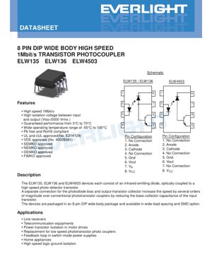
3. Pin Configuration and Functional Differences
The 8-pin DIP package has a standardized pinout with a key variation between device types.
- Pins 1 & 4: No Connection (NC) on all models.
- Pins 2 & 3: Anode and Cathode of the input LED, respectively.
- Pin 5: Ground (GND) for the output side.
- Pin 6: Output voltage (VOUT), the collector of the phototransistor.
- Pin 7: This pin differs. For ELW135 and ELW136, it is the photodiode bias voltage (VB). Connecting this pin is essential for achieving the high-speed operation. For the ELW4503, Pin 7 is No Connection (NC). The high-speed biasing is likely handled internally in the ELW4503.
- Pin 8: Supply voltage (VCC) for the output side.
The schematic diagrams show the internal connection: the photodiode (which drives the transistor's base) is connected between Pin 7 (VB) and Pin 6 (VOUT/Collector). The phototransistor's emitter is connected to Pin 5 (GND).
4. Application Suggestions
4.1 Typical Application Circuits
These photocouplers are ideal for digital signal isolation. A typical circuit involves connecting the input LED in series with a current-limiting resistor to a microcontroller or logic gate output. On the output side, a pull-up resistor (RL) is connected between VCC (Pin 8) and VOUT (Pin 6). The value of RL must be chosen based on the desired switching speed, output current, and the device's CTR, as specified in the datasheet tables (e.g., 4.1 kΩ for ELW135, 1.9 kΩ for ELW136/4503 for the switching tests). For the ELW135/136, Pin 7 (VB) must be connected, often to VCC through a resistor or directly, depending on the desired biasing for speed vs. sensitivity.
4.2 Design Considerations and Notes
- Speed vs. CTR Trade-off: The separate base connection (Pin 7) allows trading off some CTR for higher speed by adjusting the photodiode bias. The datasheet switching specs are given for a specific condition.
- Model Selection: Choose ELW135 for general-purpose, cost-sensitive 1Mbit/s applications. ELW136 offers higher minimum CTR for better margin in designs requiring more output current drive. ELW4503 is the premium choice for environments with extremely high electrical noise (e.g., industrial motor controls, power inverters) due to its exceptional 15,000+ V/µs CMTI.
- Power Dissipation: Ensure the input power (IF * VF) does not exceed 45 mW and the output power does not exceed 100 mW, considering ambient temperature.
- Layout for Isolation: To maintain the high isolation rating, ensure adequate creepage and clearance distances on the PCB between the input-side traces (pins 1-4) and output-side traces (pins 5-8). A slot or barrier in the PCB under the device is often recommended.
5. Packaging and Ordering Information
The devices are available in different packaging options denoted by a suffix in the part number.
Part Number Format: ELW13XY(Z)-V or ELW4503Y(Z)-V
- X = Part number identifier (5 for ELW135, 6 for ELW136).
- Y = Lead form option: 'S' for surface mount lead form, blank for standard DIP.
- Z = Tape and reel option: 'TA' or 'TB', blank for tube packaging.
- V = Optional VDE approval marking.
Packing Quantities: Standard DIP-8 packages are supplied in tubes containing 40 units. The surface-mount option with tape and reel ('S(TA)') is supplied in reels containing 500 units.
6. Technical Comparison and FAQs
6.1 Differentiation Between Models
The primary differentiators are Current Transfer Ratio (CTR) and Common Mode Transient Immunity (CMTI). The ELW135 has the lowest guaranteed CTR (7-50%), the ELW136 has a higher minimum CTR (19-50%), and the ELW4503 matches the ELW136's CTR but adds a vastly superior CMTI rating (>15 kV/µs vs. 1 kV/µs). The ELW4503 also has Pin 7 as NC, simplifying the external circuit compared to the ELW135/136 which require a connection to Pin 7.
6.2 Frequently Asked Questions Based on Parameters
- Q: What is the maximum data rate achievable? A: The devices are characterized for 1 Mbit/s operation based on the propagation delay specifications. Actual maximum rate depends on the specific circuit design, including RL and input drive conditions.
- Q: Can I use a 3.3V VCC? A: The electrical characteristics are tested with VCC=4.5V and 5V. While the Absolute Max rating allows down to -0.5V, operation at 3.3V may be possible but performance (like VOL and switching times) should be verified under the actual lower VCC condition, as it is not fully characterized in the provided datasheet.
- Q: Why is Pin 7 (VB) important for ELW135/136? A: Connecting Pin 7 provides a low-impedance path to sweep out charge from the photodiode/base junction, drastically reducing the Miller capacitance effect and enabling the high-speed switching. Leaving it unconnected will result in performance similar to a slow conventional phototransistor coupler.
- Q: How do I ensure the 5000Vrms isolation in my design? A: The component itself is rated for this. The system designer must ensure the PCB layout maintains sufficient creepage/clearance (e.g., >8mm for reinforced insulation at this voltage level per safety standards) between all input and output circuits, including under the component body.
7. Operating Principle
The fundamental principle is optoelectronic isolation. An electrical signal applied to the input LED causes it to emit infrared light. This light traverses an optically transparent but electrically insulating barrier (typically a mold compound or air gap) within the package. The light is detected by a photodiode on the output side, which generates a photocurrent. In these high-speed devices, this photocurrent directly modulates the base of an integrated bipolar transistor. The key to high speed is the separate access to the photodiode (Pin 7 on ELW135/136), which allows the photodiode capacitance to be charged/discharged quickly, minimizing the storage time in the transistor and thus reducing propagation delay and rise/fall times.
LED Specification Terminology
Complete explanation of LED technical terms
Photoelectric Performance
| Term | Unit/Representation | Simple Explanation | Why Important |
|---|---|---|---|
| Luminous Efficacy | lm/W (lumens per watt) | Light output per watt of electricity, higher means more energy efficient. | Directly determines energy efficiency grade and electricity cost. |
| Luminous Flux | lm (lumens) | Total light emitted by source, commonly called "brightness". | Determines if the light is bright enough. |
| Viewing Angle | ° (degrees), e.g., 120° | Angle where light intensity drops to half, determines beam width. | Affects illumination range and uniformity. |
| CCT (Color Temperature) | K (Kelvin), e.g., 2700K/6500K | Warmth/coolness of light, lower values yellowish/warm, higher whitish/cool. | Determines lighting atmosphere and suitable scenarios. |
| CRI / Ra | Unitless, 0–100 | Ability to render object colors accurately, Ra≥80 is good. | Affects color authenticity, used in high-demand places like malls, museums. |
| SDCM | MacAdam ellipse steps, e.g., "5-step" | Color consistency metric, smaller steps mean more consistent color. | Ensures uniform color across same batch of LEDs. |
| Dominant Wavelength | nm (nanometers), e.g., 620nm (red) | Wavelength corresponding to color of colored LEDs. | Determines hue of red, yellow, green monochrome LEDs. |
| Spectral Distribution | Wavelength vs intensity curve | Shows intensity distribution across wavelengths. | Affects color rendering and quality. |
Electrical Parameters
| Term | Symbol | Simple Explanation | Design Considerations |
|---|---|---|---|
| Forward Voltage | Vf | Minimum voltage to turn on LED, like "starting threshold". | Driver voltage must be ≥Vf, voltages add up for series LEDs. |
| Forward Current | If | Current value for normal LED operation. | Usually constant current drive, current determines brightness & lifespan. |
| Max Pulse Current | Ifp | Peak current tolerable for short periods, used for dimming or flashing. | Pulse width & duty cycle must be strictly controlled to avoid damage. |
| Reverse Voltage | Vr | Max reverse voltage LED can withstand, beyond may cause breakdown. | Circuit must prevent reverse connection or voltage spikes. |
| Thermal Resistance | Rth (°C/W) | Resistance to heat transfer from chip to solder, lower is better. | High thermal resistance requires stronger heat dissipation. |
| ESD Immunity | V (HBM), e.g., 1000V | Ability to withstand electrostatic discharge, higher means less vulnerable. | Anti-static measures needed in production, especially for sensitive LEDs. |
Thermal Management & Reliability
| Term | Key Metric | Simple Explanation | Impact |
|---|---|---|---|
| Junction Temperature | Tj (°C) | Actual operating temperature inside LED chip. | Every 10°C reduction may double lifespan; too high causes light decay, color shift. |
| Lumen Depreciation | L70 / L80 (hours) | Time for brightness to drop to 70% or 80% of initial. | Directly defines LED "service life". |
| Lumen Maintenance | % (e.g., 70%) | Percentage of brightness retained after time. | Indicates brightness retention over long-term use. |
| Color Shift | Δu′v′ or MacAdam ellipse | Degree of color change during use. | Affects color consistency in lighting scenes. |
| Thermal Aging | Material degradation | Deterioration due to long-term high temperature. | May cause brightness drop, color change, or open-circuit failure. |
Packaging & Materials
| Term | Common Types | Simple Explanation | Features & Applications |
|---|---|---|---|
| Package Type | EMC, PPA, Ceramic | Housing material protecting chip, providing optical/thermal interface. | EMC: good heat resistance, low cost; Ceramic: better heat dissipation, longer life. |
| Chip Structure | Front, Flip Chip | Chip electrode arrangement. | Flip chip: better heat dissipation, higher efficacy, for high-power. |
| Phosphor Coating | YAG, Silicate, Nitride | Covers blue chip, converts some to yellow/red, mixes to white. | Different phosphors affect efficacy, CCT, and CRI. |
| Lens/Optics | Flat, Microlens, TIR | Optical structure on surface controlling light distribution. | Determines viewing angle and light distribution curve. |
Quality Control & Binning
| Term | Binning Content | Simple Explanation | Purpose |
|---|---|---|---|
| Luminous Flux Bin | Code e.g., 2G, 2H | Grouped by brightness, each group has min/max lumen values. | Ensures uniform brightness in same batch. |
| Voltage Bin | Code e.g., 6W, 6X | Grouped by forward voltage range. | Facilitates driver matching, improves system efficiency. |
| Color Bin | 5-step MacAdam ellipse | Grouped by color coordinates, ensuring tight range. | Guarantees color consistency, avoids uneven color within fixture. |
| CCT Bin | 2700K, 3000K etc. | Grouped by CCT, each has corresponding coordinate range. | Meets different scene CCT requirements. |
Testing & Certification
| Term | Standard/Test | Simple Explanation | Significance |
|---|---|---|---|
| LM-80 | Lumen maintenance test | Long-term lighting at constant temperature, recording brightness decay. | Used to estimate LED life (with TM-21). |
| TM-21 | Life estimation standard | Estimates life under actual conditions based on LM-80 data. | Provides scientific life prediction. |
| IESNA | Illuminating Engineering Society | Covers optical, electrical, thermal test methods. | Industry-recognized test basis. |
| RoHS / REACH | Environmental certification | Ensures no harmful substances (lead, mercury). | Market access requirement internationally. |
| ENERGY STAR / DLC | Energy efficiency certification | Energy efficiency and performance certification for lighting. | Used in government procurement, subsidy programs, enhances competitiveness. |