Table of Contents
- 1. Product Overview
- 1.1 Core Advantages and Target Market
- 2. In-Depth Technical Parameter Analysis
- 2.1 Absolute Maximum Ratings
- 2.2 Electrical Characteristics
- 2.3 Switching Characteristics
- 3. Mechanical and Package Information
- 3.1 Package Dimensions and Pin Configuration
- 3.2 Recommended Pad Layout and Polarity Identification
- 4. Soldering and Assembly Guidelines
- 5. Packaging and Ordering Information
- 6. Application Suggestions and Design Considerations
- 6.1 Typical Application Circuits
- 6.2 Design Considerations
- 7. Technical Comparison and Differentiation
- 8. Frequently Asked Questions (FAQ)
- 9. Practical Application Example
- 10. Operating Principle
- 11. Technology Trends
- LED Specification Terminology
- Photoelectric Performance
- Electrical Parameters
- Thermal Management & Reliability
- Packaging & Materials
- Quality Control & Binning
- Testing & Certification
1. Product Overview
The ELM453L is a high-speed transistor photocoupler (optoisolator) designed for applications requiring fast digital signal isolation. It integrates an infrared emitting diode optically coupled to a high-speed photodetector transistor. A key architectural feature is the separate connection for the photodiode bias and the output transistor's collector. This design significantly reduces the base-collector capacitance of the input transistor, enabling switching speeds several orders of magnitude faster than conventional phototransistor couplers. The device is housed in a compact, industry-standard 5-pin Small Outline Package (SOP), making it suitable for automated surface mount technology (SMT) assembly processes.
1.1 Core Advantages and Target Market
The primary advantages of the ELM453L include its high-speed capability of 1 Megabit per second (1Mbit/s), operation from a low 3.3V supply voltage, and robust isolation characteristics. It features a high isolation voltage of 3750 Vrms between input and output, and excellent Common Mode Rejection (CMR) of 15 kV/μs. These characteristics make it an ideal solution for industrial communication and control systems where noise immunity and safety are critical. The device is guaranteed to perform from 0°C to 70°C and has an extended operating temperature range of -40°C to 85°C, supporting applications in harsh environments. It complies with major international safety standards (UL, cUL, VDE) and environmental regulations (RoHS, Halogen Free, REACH).
The target applications are primarily in industrial automation and power electronics. Key use cases include line receivers for serial communication, field bus interfaces (like Profibus, CAN), providing isolation for power transistors in motor drives, and replacing slower phototransistor couplers in legacy designs. It is also suitable for high-speed logic ground isolation and analog signal ground isolation in mixed-signal systems.
2. In-Depth Technical Parameter Analysis
2.1 Absolute Maximum Ratings
The Absolute Maximum Ratings define the stress limits beyond which permanent damage to the device may occur. For the input side (LED), the continuous forward current (IF) must not exceed 25 mA, with a peak forward current (IFP) of 50 mA allowed under pulsed conditions (50% duty cycle, 1ms pulse width). A very high transient current (IFtrans) of 1A is permissible for very short pulses (1μs, 300 pps), which is relevant for withstanding brief surges. The reverse voltage (VR) on the LED is limited to 5V. On the output side, the average output current (IO(AVG)) is rated at 8 mA, with a peak of 16 mA. The output voltage (VO) can range from -0.5V to 20V, and the supply voltage (VCC) from -0.5V to 30V. The device can withstand an isolation voltage (VISO) of 3750 Vrms applied for one minute between the input and output sides under specified humidity conditions.
2.2 Electrical Characteristics
The Electrical Characteristics are guaranteed over the operating temperature range of 0°C to 70°C unless otherwise noted.
Input Characteristics: The forward voltage (VF) of the infrared LED is typically 1.45V at a forward current (IF) of 16 mA, with a maximum of 1.8V. This low VF contributes to lower power dissipation. The temperature coefficient of VF is approximately -1.6 mV/°C, meaning VF decreases slightly as temperature increases.
Output Characteristics: The logic high output current (IOH), which is the leakage current when the LED is off, is very low (typically 0.001 μA at VCC=3.3V). The supply current differs significantly between logic states. The logic low supply current (ICCL) is typically 100 μA when the LED is on (IF=16mA), whereas the logic high supply current (ICCH) is typically only 0.05 μA when the LED is off. This highlights the device's low power consumption in the idle state.
Transfer Characteristics: The Current Transfer Ratio (CTR) is a critical parameter, defined as the ratio of the output transistor's collector current to the input LED's forward current, expressed as a percentage. For the ELM453L, the CTR is between 20% and 50% under standard test conditions (IF=16mA, VO=0.4V, VCC=3.3V, TA=25°C). The minimum CTR is guaranteed to be 15% under slightly different conditions (VO=0.5V). The logic low output voltage (VOL) is guaranteed to be below 0.4V when sinking 3mA, and below 0.5V when sinking 1.1mA, ensuring solid logic-low levels for 3.3V systems.
2.3 Switching Characteristics
Switching performance is tested with VCC=3.3V and a load resistor (RL) of 1.9 kΩ. The propagation delay time to logic low (tPHL) is typically 0.3 μs (max 1.0 μs), and the propagation delay time to logic high (tPLH) is typically 0.65 μs (max 1.0 μs). These symmetrical delays support reliable data transmission at 1Mbit/s. A standout feature is the Common Mode Transient Immunity (CMTI), which is the device's ability to reject fast voltage transients between the input and output grounds. Both CMTI at logic high (CMH) and at logic low (CML) are specified at a minimum of 15,000 V/μs with a common-mode pulse (VCM) of 1500V peak-to-peak. This extremely high CMTI is essential for reliable operation in noisy industrial environments with switching power supplies and motor drives.
3. Mechanical and Package Information
3.1 Package Dimensions and Pin Configuration
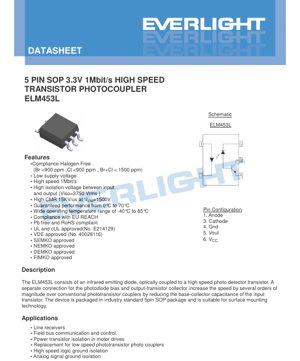
The ELM453L is packaged in a 5-pin Small Outline Package (SOP). The package body dimensions are approximately 4.9 mm in length, 6.0 mm in width, and 1.75 mm in height (excluding leads). The pin configuration is as follows: Pin 1: Anode of the input LED; Pin 3: Cathode of the input LED; Pin 4: Ground (GND) for the output side; Pin 5: Output Voltage (VOUT); Pin 6: Supply Voltage (VCC) for the output side. Note that Pin 2 is not present or not connected in this package configuration.
3.2 Recommended Pad Layout and Polarity Identification
The datasheet provides a recommended land pattern (footprint) for PCB design to ensure reliable soldering. The pad layout accounts for the package dimensions and lead pitch. The device marking on the top of the package includes the manufacturer's logo abbreviation, the device number (M453L), a 1-digit year code (Y), a 2-digit week code (WW), and an optional code (V) indicating VDE approval. Correct orientation during assembly is crucial and can be identified by the marking and the package notch.
4. Soldering and Assembly Guidelines
The device is rated for a maximum soldering temperature (TSOL) of 260°C for 10 seconds. This is compatible with standard lead-free reflow soldering profiles. It is critical to follow the recommended pad layout to prevent tombstoning or poor solder joints. The device should be stored in conditions between -55°C and 125°C and in a dry environment to prevent moisture absorption, which can cause popcorning during reflow.
5. Packaging and Ordering Information
The ELM453L is available in different packaging options. The standard version is supplied in tubes containing 100 units. For high-volume automated assembly, it is available on tape and reel. Two reel options are offered: TA and TB, each containing 3000 units per reel. An optional suffix \"-V\" indicates units that are VDE approved. The full part number format is ELM453L(Z)-V, where (Z) represents the tape and reel option (TA, TB, or none).
6. Application Suggestions and Design Considerations
6.1 Typical Application Circuits
The primary application is as a digital isolator in serial communication lines. A typical circuit involves connecting the input LED in series with a current-limiting resistor to a microcontroller's GPIO pin. The output transistor operates as a common-emitter switch, with a pull-up resistor (RL) connected between VCC (Pin 6) and the output collector (Pin 5). The value of RL affects both the output logic levels and the switching speed; the test condition of 1.9 kΩ is a good starting point for 3.3V systems. For driving higher loads, ensure the output current (IO) does not exceed the absolute maximum ratings.
6.2 Design Considerations
Power Supply Decoupling: Place a 0.1 μF ceramic capacitor close to the VCC pin (Pin 6) and ground (Pin 4) to minimize noise on the output side supply.
LED Current Setting: The forward current (IF) directly impacts CTR, switching speed, and power consumption. The datasheet uses IF=16mA for most specifications. The current-limiting resistor value can be calculated as R = (VDRIVE - VF) / IF, where VDRIVE is the driving voltage (e.g., 3.3V) and VF is approximately 1.45V.
Layout for High CMTI: To maintain the high common-mode transient immunity, minimize the parasitic capacitance between the input and output sections of the PCB layout. Provide a clear isolation gap (creepage and clearance distance) as per safety standards, and avoid routing input and output traces parallel or overlapping on adjacent PCB layers.
7. Technical Comparison and Differentiation
Compared to standard phototransistor couplers, the ELM453L's dedicated photodiode bias pin (which is internally connected) is the key differentiator. In a standard phototransistor, the base-collector junction also acts as the photodiode, creating a large capacitance that limits speed. By separating these functions, the ELM453L achieves much faster switching (1Mbit/s vs. typically 10-100 kbit/s for standard types). Compared to more advanced digital isolators using CMOS technology, this transistor-based photocoupler offers higher isolation voltage and proven long-term reliability in harsh environments, though at the cost of higher power consumption and slower maximum speed.
8. Frequently Asked Questions (FAQ)
Q: Can I use this device with a 5V supply (VCC)?
A: Yes, the Absolute Maximum Rating for VCC is 30V, and the electrical characteristics are also provided for VCC=15V. However, the switching characteristics are specifically characterized at VCC=3.3V. For 5V operation, you may need to adjust the pull-up resistor RL to maintain proper output current levels, and performance should be validated.
Q: What is the purpose of the separate GND (Pin 4) and VCC (Pin 6) pins on the output side?
A> This allows for flexible biasing of the internal photodiode and the output transistor independently, which is part of the architecture that enables high speed. In typical use, they are connected to the same output-side power rail and ground plane, but the separation is crucial internally.
Q: How do I ensure the 15 kV/μs CMTI in my design?
A> The CMTI is an intrinsic device characteristic. To realize it in your system, you must design the PCB layout to prevent external noise from coupling into the isolation barrier. This involves maintaining a clean isolation gap, using guard rings if necessary, and proper grounding and shielding techniques on both sides of the isolator.
9. Practical Application Example
Scenario: Isolating a RS-485 Transceiver in a Motor Control Cabinet. In this noisy environment, a microcontroller needs to communicate with a remote RS-485 network. The TX and RX lines from the microcontroller are connected to a local RS-485 transceiver chip. The differential A/B lines from this transceiver then connect to the network. To protect the sensitive microcontroller from ground potential differences and high-voltage transients on the network side, the ELM453L can be used to isolate the TX and RX signals between the microcontroller and the transceiver. Two ELM453L units would be used: one for the TX direction and one for the RX direction. The high CMTI (15 kV/μs) ensures that the rapid voltage swings caused by the motor's inverter do not corrupt the digital communication. The 1Mbit/s speed is sufficient for common industrial fieldbus protocols like Modbus RTU.
10. Operating Principle
The fundamental principle is optoelectronic isolation. An electrical signal applied to the input side causes the infrared Light Emitting Diode (LED) to emit light proportional to the current. This light travels across a transparent isolation barrier (typically a molded plastic gap). On the output side, a photodiode detects this light and generates a photocurrent. In the ELM453L, this photocurrent is used to bias a high-speed transistor amplifier. The separate connection for the photodiode allows the photocurrent to be efficiently injected into the base of the transistor while minimizing parasitic capacitance, enabling fast switching of the transistor's collector-emitter path. Thus, the input electrical signal is converted to light, transmitted across an electrically insulating barrier, and reconverted into an electrical signal on the output, providing galvanic isolation.
11. Technology Trends
The market for optocouplers continues to evolve. Key trends include demands for higher data rates (>10 Mbit/s) to support faster industrial Ethernet protocols, which is being addressed by newer architectures like digital isolators based on RF or capacitive coupling. There is also a push for higher integration, combining multiple isolation channels or integrating isolation with other functions like ADC drivers or gate drivers into a single package. Furthermore, increasing demands for system-level reliability and longevity in automotive and industrial applications drive the need for components with higher temperature ratings and proven robustness under extended stress conditions. Devices like the ELM453L, which offer a balance of speed, high isolation voltage, and proven reliability, remain highly relevant in applications where these latter characteristics are prioritized over ultimate speed.
LED Specification Terminology
Complete explanation of LED technical terms
Photoelectric Performance
| Term | Unit/Representation | Simple Explanation | Why Important |
|---|---|---|---|
| Luminous Efficacy | lm/W (lumens per watt) | Light output per watt of electricity, higher means more energy efficient. | Directly determines energy efficiency grade and electricity cost. |
| Luminous Flux | lm (lumens) | Total light emitted by source, commonly called "brightness". | Determines if the light is bright enough. |
| Viewing Angle | ° (degrees), e.g., 120° | Angle where light intensity drops to half, determines beam width. | Affects illumination range and uniformity. |
| CCT (Color Temperature) | K (Kelvin), e.g., 2700K/6500K | Warmth/coolness of light, lower values yellowish/warm, higher whitish/cool. | Determines lighting atmosphere and suitable scenarios. |
| CRI / Ra | Unitless, 0–100 | Ability to render object colors accurately, Ra≥80 is good. | Affects color authenticity, used in high-demand places like malls, museums. |
| SDCM | MacAdam ellipse steps, e.g., "5-step" | Color consistency metric, smaller steps mean more consistent color. | Ensures uniform color across same batch of LEDs. |
| Dominant Wavelength | nm (nanometers), e.g., 620nm (red) | Wavelength corresponding to color of colored LEDs. | Determines hue of red, yellow, green monochrome LEDs. |
| Spectral Distribution | Wavelength vs intensity curve | Shows intensity distribution across wavelengths. | Affects color rendering and quality. |
Electrical Parameters
| Term | Symbol | Simple Explanation | Design Considerations |
|---|---|---|---|
| Forward Voltage | Vf | Minimum voltage to turn on LED, like "starting threshold". | Driver voltage must be ≥Vf, voltages add up for series LEDs. |
| Forward Current | If | Current value for normal LED operation. | Usually constant current drive, current determines brightness & lifespan. |
| Max Pulse Current | Ifp | Peak current tolerable for short periods, used for dimming or flashing. | Pulse width & duty cycle must be strictly controlled to avoid damage. |
| Reverse Voltage | Vr | Max reverse voltage LED can withstand, beyond may cause breakdown. | Circuit must prevent reverse connection or voltage spikes. |
| Thermal Resistance | Rth (°C/W) | Resistance to heat transfer from chip to solder, lower is better. | High thermal resistance requires stronger heat dissipation. |
| ESD Immunity | V (HBM), e.g., 1000V | Ability to withstand electrostatic discharge, higher means less vulnerable. | Anti-static measures needed in production, especially for sensitive LEDs. |
Thermal Management & Reliability
| Term | Key Metric | Simple Explanation | Impact |
|---|---|---|---|
| Junction Temperature | Tj (°C) | Actual operating temperature inside LED chip. | Every 10°C reduction may double lifespan; too high causes light decay, color shift. |
| Lumen Depreciation | L70 / L80 (hours) | Time for brightness to drop to 70% or 80% of initial. | Directly defines LED "service life". |
| Lumen Maintenance | % (e.g., 70%) | Percentage of brightness retained after time. | Indicates brightness retention over long-term use. |
| Color Shift | Δu′v′ or MacAdam ellipse | Degree of color change during use. | Affects color consistency in lighting scenes. |
| Thermal Aging | Material degradation | Deterioration due to long-term high temperature. | May cause brightness drop, color change, or open-circuit failure. |
Packaging & Materials
| Term | Common Types | Simple Explanation | Features & Applications |
|---|---|---|---|
| Package Type | EMC, PPA, Ceramic | Housing material protecting chip, providing optical/thermal interface. | EMC: good heat resistance, low cost; Ceramic: better heat dissipation, longer life. |
| Chip Structure | Front, Flip Chip | Chip electrode arrangement. | Flip chip: better heat dissipation, higher efficacy, for high-power. |
| Phosphor Coating | YAG, Silicate, Nitride | Covers blue chip, converts some to yellow/red, mixes to white. | Different phosphors affect efficacy, CCT, and CRI. |
| Lens/Optics | Flat, Microlens, TIR | Optical structure on surface controlling light distribution. | Determines viewing angle and light distribution curve. |
Quality Control & Binning
| Term | Binning Content | Simple Explanation | Purpose |
|---|---|---|---|
| Luminous Flux Bin | Code e.g., 2G, 2H | Grouped by brightness, each group has min/max lumen values. | Ensures uniform brightness in same batch. |
| Voltage Bin | Code e.g., 6W, 6X | Grouped by forward voltage range. | Facilitates driver matching, improves system efficiency. |
| Color Bin | 5-step MacAdam ellipse | Grouped by color coordinates, ensuring tight range. | Guarantees color consistency, avoids uneven color within fixture. |
| CCT Bin | 2700K, 3000K etc. | Grouped by CCT, each has corresponding coordinate range. | Meets different scene CCT requirements. |
Testing & Certification
| Term | Standard/Test | Simple Explanation | Significance |
|---|---|---|---|
| LM-80 | Lumen maintenance test | Long-term lighting at constant temperature, recording brightness decay. | Used to estimate LED life (with TM-21). |
| TM-21 | Life estimation standard | Estimates life under actual conditions based on LM-80 data. | Provides scientific life prediction. |
| IESNA | Illuminating Engineering Society | Covers optical, electrical, thermal test methods. | Industry-recognized test basis. |
| RoHS / REACH | Environmental certification | Ensures no harmful substances (lead, mercury). | Market access requirement internationally. |
| ENERGY STAR / DLC | Energy efficiency certification | Energy efficiency and performance certification for lighting. | Used in government procurement, subsidy programs, enhances competitiveness. |