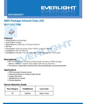
1. Product Overview
The IR17-21C/TR8 is a high-performance infrared (IR) emitting diode designed for modern surface-mount technology (SMT) applications. Housed in a compact 0805 package, this device is engineered to deliver reliable infrared emission specifically matched to silicon-based photodetectors. Its primary function is to serve as an efficient infrared source in various sensing and switching circuits.
The core advantage of this component lies in its miniature form factor, which allows for high-density PCB designs, and its excellent spectral matching to silicon photodiodes and phototransistors, ensuring optimal system sensitivity. The device is constructed with a water-clear plastic lens, providing a flat top view which contributes to its wide 120-degree viewing angle. It is compliant with key environmental and safety standards, including RoHS, EU REACH, and is manufactured as a halogen-free component.
2. Technical Specifications and Objective Interpretation
2.1 Absolute Maximum Ratings
These ratings define the stress limits beyond which permanent damage to the device may occur. Operation under or at these limits is not guaranteed.
- Continuous Forward Current (IF): 65 mA. This is the maximum DC current that can continuously flow through the LED.
- Reverse Voltage (VR): 5 V. Applying a reverse bias voltage higher than this can break down the LED's PN junction.
- Operating & Storage Temperature (Topr, Tstg): -40°C to +85°C. The device is rated for industrial temperature ranges.
- Power Dissipation (Pd): 130 mW at 25°C. This is the maximum power the package can dissipate as heat. Derating is necessary at higher ambient temperatures.
- Soldering Temperature (Tsol): 260°C for ≤5 seconds. This defines the peak reflow profile tolerance.
2.2 Electro-Optical Characteristics
These parameters are measured at a standard test condition of 25°C ambient temperature and a forward current of 20 mA, representing typical operating conditions.
- Radiant Intensity (Ie): 0.2 mW/sr (Min), 0.8 mW/sr (Typ). This measures the optical power emitted per unit solid angle. The typical value indicates the expected output.
- Peak Wavelength (λp): 940 nm (Typ). The infrared light emitted is centered at this wavelength, which is ideal for silicon detectors that have high sensitivity in the near-infrared region.
- Spectral Bandwidth (Δλ): 45 nm (Typ). This defines the range of wavelengths emitted, typically Full Width at Half Maximum (FWHM).
- Forward Voltage (VF): 1.2 V (Typ), 1.5 V (Max) at 20mA. The low forward voltage reduces power consumption and thermal load.
- Reverse Current (IR): 10 µA (Max) at 5V. This is the leakage current when the device is reverse-biased.
- Viewing Angle (2θ1/2): 120° (Typ). Defined as the full angle where intensity drops to half of the on-axis value, providing a very wide emission pattern.
3. Performance Curve Analysis
The datasheet provides several characteristic curves that are crucial for design engineers.
- Forward Current vs. Ambient Temperature: This graph shows how the maximum allowable forward current decreases as the ambient temperature increases, due to the power dissipation limit of the package. It is essential for thermal management.
- Spectral Distribution: Illustrates the relative radiant power as a function of wavelength, confirming the peak at 940nm and the spectral bandwidth.
- Forward Current vs. Forward Voltage (I-V Curve): Demonstrates the exponential relationship typical of a diode. The curve helps in selecting the appropriate current-limiting resistor for a given supply voltage.
- Relative Radiant Intensity vs. Angular Displacement: A polar plot showing the emission pattern. The 120-degree viewing angle is visually confirmed here, showing a Lambertian or near-Lambertian distribution common for flat-top LEDs.
4. Mechanical and Packaging Information
4.1 Package Dimensions
The IR17-21C/TR8 conforms to the standard 0805 (Imperial) or 2012 (Metric) footprint. Key dimensions include a body length of approximately 2.0 mm, a width of 1.25 mm, and a height of typically 0.8 to 1.0 mm (exact value from drawing). The anode and cathode are clearly marked on the package. The suggested pad layout is provided for PCB design, with recommendations to adjust based on specific manufacturing processes.
4.2 Carrier Taping Dimensions
The components are supplied on standard 8mm tape reels for automated pick-and-place assembly. Each reel contains 3000 pieces. The tape dimensions, including pocket size, pitch, and reel diameter, are specified to ensure compatibility with SMT equipment feeders.
5. Soldering and Assembly Guidelines
5.1 Moisture Sensitivity and Storage
The device is moisture-sensitive (MSL level specified on label). Unopened moisture barrier bags must be stored below 30°C and 90% RH. Once opened, components have a floor life of 168 hours (7 days) when stored at ≤60% RH. Exceeding this requires a baking procedure (e.g., 96 hours at 60°C) before reflow to prevent \"popcorning\" damage during soldering.
5.2 Reflow Soldering Profile
A lead-free (Pb-free) reflow temperature profile is recommended. Key parameters include a preheat stage, a defined time above liquidus (e.g., 217°C), a peak temperature not exceeding 260°C, and a total time within the critical temperature zone. Reflow should not be performed more than two times.
5.3 Hand Soldering and Rework
If hand soldering is necessary, a soldering iron with a tip temperature below 350°C and a power rating under 25W should be used. Contact time per terminal should be limited to 3 seconds, with adequate cooling between terminals. For rework, a dual-head soldering iron is recommended to simultaneously heat both terminals and avoid mechanical stress on the solder joints. The impact of rework on device reliability should be evaluated beforehand.
6. Application Suggestions and Design Considerations
6.1 Typical Application Scenarios
- PCB-Mounted Infrared Sensors: Used as the emitter in proximity sensors, object detection, and touchless switches.
- Miniature Light Barriers / Optical Interrupters: Paired with a photodetector to detect objects breaking a light beam, used in encoders, slot sensors, and security systems.
- Optoelectronic Switches: In reflective sensors where the LED light bounces off a surface back to a detector.
- Smoke Detectors: Employed in some optical chamber designs to detect smoke particles scattering light.
6.2 Critical Design Considerations
- Current Limiting is Mandatory: An external series resistor must always be used to set the forward current. The LED's low forward voltage means even small increases in supply voltage can cause a large, destructive increase in current.
- Thermal Management: While the package is small, power dissipation must be considered, especially in high-ambient-temperature environments or when driving near maximum current. Adequate PCB copper area can help dissipate heat.
- Optical Alignment: The wide 120-degree viewing angle is beneficial for broad coverage but reduces the intensity at any specific point. For longer-range or focused applications, external lenses may be required.
- Electrical Noise Immunity: In electrically noisy environments, consider shielding or modulating the LED drive current to distinguish the signal from ambient IR noise (e.g., from sunlight or other sources).
7. Technical Comparison and Differentiation
Compared to other infrared LEDs, the IR17-21C/TR8's key differentiators are its combination of a very compact 0805 footprint with a relatively high radiant intensity (0.8 mW/sr typical) and a wide 120-degree viewing angle. Many competing IR LEDs in similar packages may offer narrower viewing angles or lower output. Its low forward voltage of 1.2V is also an advantage for low-voltage battery-operated circuits, improving efficiency. The explicit compliance with Halogen-Free and REACH standards makes it suitable for environmentally conscious designs with strict material restrictions.
8. Frequently Asked Questions (Based on Technical Parameters)
8.1 What resistor value should I use to drive this LED at 20mA from a 5V supply?
Using Ohm's Law: R = (Vsupply - VF) / IF. With Vsupply=5V, VF=1.2V (typical), and IF=0.020A, R = (5 - 1.2) / 0.02 = 190 Ohms. A standard 200 Ohm resistor would result in a current of approximately (5-1.2)/200 = 19mA, which is acceptable. Always calculate using the maximum VF (1.5V) to ensure the minimum current is sufficient for your application.
8.2 Can I pulse this LED with currents higher than 65mA?
The Absolute Maximum Rating for Continuous Forward Current is 65mA. Pulsing with higher peak currents may be possible if the duty cycle is low enough to keep the average current and the resulting junction temperature within safe limits. However, the datasheet does not provide pulsed current ratings or derating curves. Operating above the absolute maximum ratings is not recommended without specific characterization data from the manufacturer, as it can reduce reliability and lifetime.
8.3 How does ambient temperature affect the output?
The radiant intensity of LEDs typically decreases as junction temperature increases. The \"Forward Current vs. Ambient Temperature\" graph indirectly relates to this, as higher temperatures force a reduction in allowable current to avoid overheating. For precise output stability over temperature, a feedback circuit using the paired photodetector or temperature compensation may be necessary.
9. Practical Design and Usage Case
Case: Designing a Paper Detection Sensor in a Printer
An engineer needs to detect the presence of paper at the input tray of a small printer. Space is extremely limited. They choose the IR17-21C/TR8 and a matching phototransistor in a similar package. The components are placed on opposite sides of a narrow channel through which the paper passes. The LED is driven at 15mA (using a suitable resistor from the printer's 3.3V logic supply) to conserve power while providing adequate signal. The wide 120-degree viewing angle of the LED ensures the beam sufficiently fills the channel even with minor mechanical misalignment. When paper is present, it blocks the infrared light, causing a change in the phototransistor's output, which is read by a microcontroller. The low profile of the 0805 package allows the sensor to be integrated into the slim mechanism. The designer follows the reflow profile guidelines and ensures the PCB layout includes thermal relief pads for soldering.
10. Operating Principle Introduction
An Infrared Light Emitting Diode (IR LED) is a semiconductor diode. When a forward voltage is applied across its terminals (anode positive relative to cathode), electrons are injected across the PN junction. As these electrons recombine with holes in the active region of the semiconductor material (Gallium Aluminum Arsenide - GaAlAs in this case), energy is released in the form of photons (light particles). The specific composition of the GaAlAs material determines the wavelength of the emitted photons, which is in the infrared spectrum (940nm) for this device. This wavelength is invisible to the human eye but can be efficiently detected by silicon-based photodiodes and phototransistors, which generate a current when struck by photons of sufficient energy.
11. Industry Trends and Developments
The trend in optoelectronics, including IR components, continues toward miniaturization, higher efficiency, and integration. Packages smaller than 0805 (e.g., 0603, 0402) are becoming more common for space-constrained applications. There is also a drive to increase radiant intensity and power output from smaller packages through improved chip design and packaging materials. Integration is another key trend, with combined emitter-detector pairs in single packages (opto-couplers, reflective sensors) simplifying assembly and improving alignment. Furthermore, the demand for components compliant with stringent environmental regulations (RoHS, REACH, Halogen-Free) is now a standard requirement across the industry, driving material science innovations in lead-free solders and encapsulation compounds.
LED Specification Terminology
Complete explanation of LED technical terms
Photoelectric Performance
| Term | Unit/Representation | Simple Explanation | Why Important |
|---|---|---|---|
| Luminous Efficacy | lm/W (lumens per watt) | Light output per watt of electricity, higher means more energy efficient. | Directly determines energy efficiency grade and electricity cost. |
| Luminous Flux | lm (lumens) | Total light emitted by source, commonly called "brightness". | Determines if the light is bright enough. |
| Viewing Angle | ° (degrees), e.g., 120° | Angle where light intensity drops to half, determines beam width. | Affects illumination range and uniformity. |
| CCT (Color Temperature) | K (Kelvin), e.g., 2700K/6500K | Warmth/coolness of light, lower values yellowish/warm, higher whitish/cool. | Determines lighting atmosphere and suitable scenarios. |
| CRI / Ra | Unitless, 0–100 | Ability to render object colors accurately, Ra≥80 is good. | Affects color authenticity, used in high-demand places like malls, museums. |
| SDCM | MacAdam ellipse steps, e.g., "5-step" | Color consistency metric, smaller steps mean more consistent color. | Ensures uniform color across same batch of LEDs. |
| Dominant Wavelength | nm (nanometers), e.g., 620nm (red) | Wavelength corresponding to color of colored LEDs. | Determines hue of red, yellow, green monochrome LEDs. |
| Spectral Distribution | Wavelength vs intensity curve | Shows intensity distribution across wavelengths. | Affects color rendering and quality. |
Electrical Parameters
| Term | Symbol | Simple Explanation | Design Considerations |
|---|---|---|---|
| Forward Voltage | Vf | Minimum voltage to turn on LED, like "starting threshold". | Driver voltage must be ≥Vf, voltages add up for series LEDs. |
| Forward Current | If | Current value for normal LED operation. | Usually constant current drive, current determines brightness & lifespan. |
| Max Pulse Current | Ifp | Peak current tolerable for short periods, used for dimming or flashing. | Pulse width & duty cycle must be strictly controlled to avoid damage. |
| Reverse Voltage | Vr | Max reverse voltage LED can withstand, beyond may cause breakdown. | Circuit must prevent reverse connection or voltage spikes. |
| Thermal Resistance | Rth (°C/W) | Resistance to heat transfer from chip to solder, lower is better. | High thermal resistance requires stronger heat dissipation. |
| ESD Immunity | V (HBM), e.g., 1000V | Ability to withstand electrostatic discharge, higher means less vulnerable. | Anti-static measures needed in production, especially for sensitive LEDs. |
Thermal Management & Reliability
| Term | Key Metric | Simple Explanation | Impact |
|---|---|---|---|
| Junction Temperature | Tj (°C) | Actual operating temperature inside LED chip. | Every 10°C reduction may double lifespan; too high causes light decay, color shift. |
| Lumen Depreciation | L70 / L80 (hours) | Time for brightness to drop to 70% or 80% of initial. | Directly defines LED "service life". |
| Lumen Maintenance | % (e.g., 70%) | Percentage of brightness retained after time. | Indicates brightness retention over long-term use. |
| Color Shift | Δu′v′ or MacAdam ellipse | Degree of color change during use. | Affects color consistency in lighting scenes. |
| Thermal Aging | Material degradation | Deterioration due to long-term high temperature. | May cause brightness drop, color change, or open-circuit failure. |
Packaging & Materials
| Term | Common Types | Simple Explanation | Features & Applications |
|---|---|---|---|
| Package Type | EMC, PPA, Ceramic | Housing material protecting chip, providing optical/thermal interface. | EMC: good heat resistance, low cost; Ceramic: better heat dissipation, longer life. |
| Chip Structure | Front, Flip Chip | Chip electrode arrangement. | Flip chip: better heat dissipation, higher efficacy, for high-power. |
| Phosphor Coating | YAG, Silicate, Nitride | Covers blue chip, converts some to yellow/red, mixes to white. | Different phosphors affect efficacy, CCT, and CRI. |
| Lens/Optics | Flat, Microlens, TIR | Optical structure on surface controlling light distribution. | Determines viewing angle and light distribution curve. |
Quality Control & Binning
| Term | Binning Content | Simple Explanation | Purpose |
|---|---|---|---|
| Luminous Flux Bin | Code e.g., 2G, 2H | Grouped by brightness, each group has min/max lumen values. | Ensures uniform brightness in same batch. |
| Voltage Bin | Code e.g., 6W, 6X | Grouped by forward voltage range. | Facilitates driver matching, improves system efficiency. |
| Color Bin | 5-step MacAdam ellipse | Grouped by color coordinates, ensuring tight range. | Guarantees color consistency, avoids uneven color within fixture. |
| CCT Bin | 2700K, 3000K etc. | Grouped by CCT, each has corresponding coordinate range. | Meets different scene CCT requirements. |
Testing & Certification
| Term | Standard/Test | Simple Explanation | Significance |
|---|---|---|---|
| LM-80 | Lumen maintenance test | Long-term lighting at constant temperature, recording brightness decay. | Used to estimate LED life (with TM-21). |
| TM-21 | Life estimation standard | Estimates life under actual conditions based on LM-80 data. | Provides scientific life prediction. |
| IESNA | Illuminating Engineering Society | Covers optical, electrical, thermal test methods. | Industry-recognized test basis. |
| RoHS / REACH | Environmental certification | Ensures no harmful substances (lead, mercury). | Market access requirement internationally. |
| ENERGY STAR / DLC | Energy efficiency certification | Energy efficiency and performance certification for lighting. | Used in government procurement, subsidy programs, enhances competitiveness. |