Table of Contents
- 1. Product Overview
- 1.1 Core Advantages
- 1.2 Target Applications
- 2. Technical Specifications
- 2.1 Absolute Maximum Ratings
- 2.2 Electro-Optical Characteristics (Ta = 25°C)
- 3. Performance Curve Analysis
- 3.1 Forward Current vs. Ambient Temperature
- 3.2 Spectral Distribution
- 3.3 Relative Intensity vs. Forward Current
- 3.4 Forward Current vs. Forward Voltage
- 3.5 Radiation Pattern
- 4. Mechanical and Packaging Information
- 4.1 Package Dimensions
- 4.2 Polarity Identification
- 5. Soldering and Assembly Guidelines
- 5.1 Storage and Handling
- 5.2 Reflow Soldering Profile
- 5.3 Hand Soldering and Rework
- 6. Packaging and Ordering Information
- 6.1 Tape and Reel Specifications
- 6.2 Label Information
- 7. Application Design Considerations
- 7.1 Current Limiting
- 7.2 Optical Design
- 7.3 Detector Pairing
- 8. Technical Comparison and Differentiation
- 9. Frequently Asked Questions (FAQ)
- 9.1 Why is a current-limiting resistor mandatory?
- 9.2 What happens if the moisture sensitivity guidelines are not followed?
- 9.3 Can this LED be used for data transmission?
- 10. Practical Design Example
- 11. Operating Principle
- 12. Technology Trends
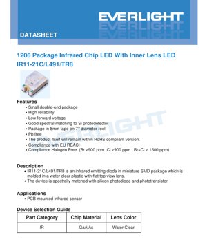
1. Product Overview
The IR11-21C/L491/TR8 is a surface-mount infrared emitting diode housed in a miniature 1206 package. It is designed with a water-clear plastic encapsulation featuring a flat top-view inner lens. The primary function of this device is to emit infrared light at a peak wavelength of 940nm, which is spectrally optimized for compatibility with common silicon-based photodetectors and phototransistors. This makes it an ideal component for non-contact sensing and detection applications.
1.1 Core Advantages
- Compact Design: The small double-ended 1206 SMD footprint allows for high-density PCB mounting, saving valuable board space.
- High Reliability: Engineered for consistent performance and long-term stability in various operating conditions.
- Optical Efficiency: The integrated inner lens provides a controlled view angle of 80 degrees, enhancing light directionality.
- Environmental Compliance: The product is lead-free, compliant with RoHS, EU REACH, and halogen-free standards (Br <900ppm, Cl <900ppm, Br+Cl <1500ppm).
- Supply Chain Friendly: Supplied on 8mm tape on 7-inch diameter reels, compatible with automated pick-and-place assembly equipment.
1.2 Target Applications
This infrared LED is primarily intended for use as a light source in PCB-mounted infrared sensor systems. Typical applications include proximity sensors, object detection, touchless switches, and optical encoders where reliable infrared emission is required.
2. Technical Specifications
2.1 Absolute Maximum Ratings
The following ratings define the limits beyond which permanent damage to the device may occur. Operation under these conditions is not guaranteed.
- Continuous Forward Current (IF): 65 mA
- Reverse Voltage (VR): 5 V
- Operating Temperature (Topr): -25°C to +85°C
- Storage Temperature (Tstg): -40°C to +85°C
- Soldering Temperature (Tsol): 260°C for ≤ 5 seconds
- Power Dissipation (Pd): 110 mW at or below 25°C free air temperature
2.2 Electro-Optical Characteristics (Ta = 25°C)
These parameters define the typical performance of the device under specified test conditions.
- Radiant Intensity (Ie): 1.0 mW/sr (Min), 2.8 mW/sr (Typ) at IF = 20mA
- Peak Wavelength (λp): 940 nm (Typ)
- Spectral Bandwidth (Δλ): 30 nm (Typ)
- Forward Voltage (VF): 1.3 V (Min), 1.7 V (Typ)
- View Angle (2θ1/2): 80 degrees (Typ)
- Reverse Current (IR): 10 µA (Max) at VR = 5V
3. Performance Curve Analysis
3.1 Forward Current vs. Ambient Temperature
Figure 1 illustrates the derating curve for the maximum allowable forward current as a function of the ambient temperature. The device can handle the full 65mA only up to approximately 25°C. As temperature increases, the maximum current must be reduced linearly to prevent overheating and ensure reliability, reaching zero at around 100°C. This graph is critical for thermal management in the application design.
3.2 Spectral Distribution
Figure 2 shows the relative radiant intensity plotted against wavelength. The curve is centered at the typical peak wavelength of 940nm with a characteristic full width at half maximum (FWHM) of approximately 30nm. This narrow bandwidth ensures efficient coupling with silicon detectors, which have peak sensitivity in the near-infrared region.
3.3 Relative Intensity vs. Forward Current
Figure 3 depicts the relationship between relative radiant intensity and forward current. The output light intensity increases with current in a generally linear fashion within the recommended operating range. This characteristic allows for simple analog or PWM-based brightness control in sensing systems.
3.4 Forward Current vs. Forward Voltage
Figure 4 is the current-voltage (I-V) characteristic curve. It shows the exponential relationship typical of a diode. The forward voltage is relatively low, around 1.7V at 20mA, which contributes to lower power consumption in the system.
3.5 Radiation Pattern
Figure 5 presents the relative radiant intensity as a function of angular displacement from the central axis (view angle). The pattern is roughly Lambertian, with intensity dropping to half its peak value at approximately ±40 degrees from the center, confirming the 80-degree full viewing angle. This pattern is important for determining the coverage area of the emitted IR light.
4. Mechanical and Packaging Information
4.1 Package Dimensions
The device conforms to a standard 1206 (3216 metric) package outline. Key dimensions are as follows:
- Length (L): 3.20 mm ± 0.10 mm
- Width (W): 1.60 mm ± 0.10 mm
- Height (H): 1.10 mm ± 0.10 mm
Detailed mechanical drawings with land pattern recommendations are provided in the datasheet for PCB layout reference. The suggested pad design ensures proper soldering and mechanical stability.
4.2 Polarity Identification
The cathode is typically marked on the device body. Consult the package drawing for the exact marking scheme to ensure correct orientation during assembly.
5. Soldering and Assembly Guidelines
5.1 Storage and Handling
The LEDs are moisture-sensitive. They must be stored in their original moisture-proof bag at 10°C to 30°C and <90% RH before use. The shelf life is one year. Once the bag is opened, the "floor life" is 168 hours (7 days) when stored at 10°C to 30°C and ≤ 60% RH. Exceeded devices require baking (e.g., 96 hours at 60°C ± 5°C, <5% RH) before reflow soldering.
5.2 Reflow Soldering Profile
A lead-free reflow soldering profile is recommended. The peak temperature should not exceed 260°C, and the time above 240°C should be controlled. Reflow should not be performed more than two times on the same device. Avoid stressing the component during heating and do not warp the PCB after soldering.
5.3 Hand Soldering and Rework
If hand soldering is necessary, use a soldering iron with a tip temperature below 350°C and a power rating under 25W. Contact time per terminal should be limited to 3 seconds. For rework, a dual-head soldering iron is suggested to simultaneously heat both terminals and avoid thermal stress. The impact of rework on device characteristics should be verified beforehand.
6. Packaging and Ordering Information
6.1 Tape and Reel Specifications
The components are supplied on 8mm wide embossed carrier tape wound on 7-inch diameter reels. Each reel contains 2000 pieces. The carrier tape dimensions (pocket pitch, width, etc.) are specified to ensure compatibility with standard SMD assembly equipment.
6.2 Label Information
The reel label includes critical information such as the part number (P/N), lot number (LOT No.), quantity (QTY), peak wavelength (HUE), rank (CAT), and moisture sensitivity level (MSL).
7. Application Design Considerations
7.1 Current Limiting
Critical: An external current-limiting resistor must always be used in series with the LED. The forward voltage has a negative temperature coefficient, meaning it decreases as the junction temperature rises. Without a resistor, a small increase in voltage can cause a large, potentially destructive, increase in current (thermal runaway). The resistor value should be calculated based on the supply voltage (VCC), the desired forward current (IF), and the typical forward voltage (VF) using Ohm's Law: R = (VCC - VF) / IF.
7.2 Optical Design
Consider the 80-degree view angle when designing lenses, apertures, or light guides for the sensor system. The radiation pattern will affect the sensing range and field of view. For longer-range detection, external collimating optics may be necessary to focus the emitted light.
7.3 Detector Pairing
This LED's 940nm output is optimally matched to the spectral response of silicon photodiodes and phototransistors. Ensure the selected detector is sensitive in this wavelength region for maximum system signal-to-noise ratio.
8. Technical Comparison and Differentiation
Compared to older through-hole IR LEDs, this 1206 SMD version offers significant advantages in miniaturization and suitability for automated manufacturing. Its key differentiators within the SMD IR LED category are its combination of a relatively high radiant intensity (2.8 mW/sr typical) with a standard, widely adopted 1206 footprint, and its compliance with stringent environmental regulations. The integrated flat lens provides a consistent optical output compared to devices without an inner lens.
9. Frequently Asked Questions (FAQ)
9.1 Why is a current-limiting resistor mandatory?
LEDs are current-driven devices, not voltage-driven. Their I-V characteristic is exponential. Operating them directly from a voltage source, even one close to their nominal VF, can lead to uncontrolled current flow, rapid heating, and immediate failure. The series resistor provides a linear, stable method to set the operating current.
9.2 What happens if the moisture sensitivity guidelines are not followed?
Moisture absorbed into the plastic package can vaporize rapidly during the high-temperature reflow soldering process. This can cause internal delamination, cracking of the package ("popcorning"), or damage to the wire bonds, leading to immediate failure or reduced long-term reliability.
9.3 Can this LED be used for data transmission?
While it emits modulated light, its primary design is for sensing applications. Its switching speed is not typically specified in this datasheet. For high-speed data transmission (e.g., IR remote controls), LEDs specifically characterized for fast response times should be selected.
10. Practical Design Example
Scenario: Designing a simple proximity sensor using this IR LED and a silicon phototransistor.
- Drive Circuit: Connect the LED anode to a 5V supply via a current-limiting resistor. For a target IF of 20mA and VF of 1.7V, calculate R = (5V - 1.7V) / 0.02A = 165Ω. Use the nearest standard value (e.g., 160Ω or 180Ω). A transistor or microcontroller GPIO pin can switch the LED on/off.
- Detection Circuit: Place the phototransistor nearby. When an object reflects the IR light back to the detector, its collector current increases. This current can be converted to a voltage using a load resistor and fed into a comparator or microcontroller ADC to detect the presence of the object.
- Layout: Place the LED and detector close together on the PCB but ensure physical barriers or optical separators are used to prevent direct crosstalk (light from the LED going straight into the detector without reflection).
11. Operating Principle
An infrared LED is a semiconductor p-n junction diode. When a forward voltage is applied, electrons from the n-region recombine with holes from the p-region in the active region. This recombination process releases energy in the form of photons (light). The specific material composition (GaAlAs in this case) determines the bandgap energy, which defines the wavelength of the emitted photons, here in the infrared spectrum at 940nm. The inner lens shapes the emitted light into a specific radiation pattern.
12. Technology Trends
The trend in infrared components for sensing continues toward higher integration, smaller packages, and improved efficiency. There is a growing demand for IR LEDs with narrower spectral bandwidths and higher output power for longer-range applications like LiDAR and time-of-flight (ToF) sensing. Furthermore, integration of the IR emitter and detector into a single module simplifies system design. Environmental and regulatory compliance remains a critical driver for all electronic components.
LED Specification Terminology
Complete explanation of LED technical terms
Photoelectric Performance
| Term | Unit/Representation | Simple Explanation | Why Important |
|---|---|---|---|
| Luminous Efficacy | lm/W (lumens per watt) | Light output per watt of electricity, higher means more energy efficient. | Directly determines energy efficiency grade and electricity cost. |
| Luminous Flux | lm (lumens) | Total light emitted by source, commonly called "brightness". | Determines if the light is bright enough. |
| Viewing Angle | ° (degrees), e.g., 120° | Angle where light intensity drops to half, determines beam width. | Affects illumination range and uniformity. |
| CCT (Color Temperature) | K (Kelvin), e.g., 2700K/6500K | Warmth/coolness of light, lower values yellowish/warm, higher whitish/cool. | Determines lighting atmosphere and suitable scenarios. |
| CRI / Ra | Unitless, 0–100 | Ability to render object colors accurately, Ra≥80 is good. | Affects color authenticity, used in high-demand places like malls, museums. |
| SDCM | MacAdam ellipse steps, e.g., "5-step" | Color consistency metric, smaller steps mean more consistent color. | Ensures uniform color across same batch of LEDs. |
| Dominant Wavelength | nm (nanometers), e.g., 620nm (red) | Wavelength corresponding to color of colored LEDs. | Determines hue of red, yellow, green monochrome LEDs. |
| Spectral Distribution | Wavelength vs intensity curve | Shows intensity distribution across wavelengths. | Affects color rendering and quality. |
Electrical Parameters
| Term | Symbol | Simple Explanation | Design Considerations |
|---|---|---|---|
| Forward Voltage | Vf | Minimum voltage to turn on LED, like "starting threshold". | Driver voltage must be ≥Vf, voltages add up for series LEDs. |
| Forward Current | If | Current value for normal LED operation. | Usually constant current drive, current determines brightness & lifespan. |
| Max Pulse Current | Ifp | Peak current tolerable for short periods, used for dimming or flashing. | Pulse width & duty cycle must be strictly controlled to avoid damage. |
| Reverse Voltage | Vr | Max reverse voltage LED can withstand, beyond may cause breakdown. | Circuit must prevent reverse connection or voltage spikes. |
| Thermal Resistance | Rth (°C/W) | Resistance to heat transfer from chip to solder, lower is better. | High thermal resistance requires stronger heat dissipation. |
| ESD Immunity | V (HBM), e.g., 1000V | Ability to withstand electrostatic discharge, higher means less vulnerable. | Anti-static measures needed in production, especially for sensitive LEDs. |
Thermal Management & Reliability
| Term | Key Metric | Simple Explanation | Impact |
|---|---|---|---|
| Junction Temperature | Tj (°C) | Actual operating temperature inside LED chip. | Every 10°C reduction may double lifespan; too high causes light decay, color shift. |
| Lumen Depreciation | L70 / L80 (hours) | Time for brightness to drop to 70% or 80% of initial. | Directly defines LED "service life". |
| Lumen Maintenance | % (e.g., 70%) | Percentage of brightness retained after time. | Indicates brightness retention over long-term use. |
| Color Shift | Δu′v′ or MacAdam ellipse | Degree of color change during use. | Affects color consistency in lighting scenes. |
| Thermal Aging | Material degradation | Deterioration due to long-term high temperature. | May cause brightness drop, color change, or open-circuit failure. |
Packaging & Materials
| Term | Common Types | Simple Explanation | Features & Applications |
|---|---|---|---|
| Package Type | EMC, PPA, Ceramic | Housing material protecting chip, providing optical/thermal interface. | EMC: good heat resistance, low cost; Ceramic: better heat dissipation, longer life. |
| Chip Structure | Front, Flip Chip | Chip electrode arrangement. | Flip chip: better heat dissipation, higher efficacy, for high-power. |
| Phosphor Coating | YAG, Silicate, Nitride | Covers blue chip, converts some to yellow/red, mixes to white. | Different phosphors affect efficacy, CCT, and CRI. |
| Lens/Optics | Flat, Microlens, TIR | Optical structure on surface controlling light distribution. | Determines viewing angle and light distribution curve. |
Quality Control & Binning
| Term | Binning Content | Simple Explanation | Purpose |
|---|---|---|---|
| Luminous Flux Bin | Code e.g., 2G, 2H | Grouped by brightness, each group has min/max lumen values. | Ensures uniform brightness in same batch. |
| Voltage Bin | Code e.g., 6W, 6X | Grouped by forward voltage range. | Facilitates driver matching, improves system efficiency. |
| Color Bin | 5-step MacAdam ellipse | Grouped by color coordinates, ensuring tight range. | Guarantees color consistency, avoids uneven color within fixture. |
| CCT Bin | 2700K, 3000K etc. | Grouped by CCT, each has corresponding coordinate range. | Meets different scene CCT requirements. |
Testing & Certification
| Term | Standard/Test | Simple Explanation | Significance |
|---|---|---|---|
| LM-80 | Lumen maintenance test | Long-term lighting at constant temperature, recording brightness decay. | Used to estimate LED life (with TM-21). |
| TM-21 | Life estimation standard | Estimates life under actual conditions based on LM-80 data. | Provides scientific life prediction. |
| IESNA | Illuminating Engineering Society | Covers optical, electrical, thermal test methods. | Industry-recognized test basis. |
| RoHS / REACH | Environmental certification | Ensures no harmful substances (lead, mercury). | Market access requirement internationally. |
| ENERGY STAR / DLC | Energy efficiency certification | Energy efficiency and performance certification for lighting. | Used in government procurement, subsidy programs, enhances competitiveness. |