Table of Contents
- 1. Product Overview
- 1.1 Core Advantages and Target Market
- 2. In-Depth Technical Parameter Analysis
- 2.1 Absolute Maximum Ratings
- 2.2 Electro-Optical Characteristics (Ta=25°C)
- 3. Performance Curve Analysis
- 3.1 Forward Current vs. Ambient Temperature
- 3.2 Spectral Distribution
- 3.3 Peak Emission Wavelength vs. Ambient Temperature
- 3.4 Forward Voltage vs. Ambient Temperature
- 3.5 Relative Radiant Intensity vs. Angular Displacement
- 4. Mechanical and Packaging Information
- 4.1 Package Dimensions (0603)
- 4.2 Polarity Identification
- 4.3 Tape and Reel Specifications
- 5. Soldering and Assembly Guidelines
- 5.1 Moisture Sensitivity and Storage
- 5.2 Reflow Soldering Profile
- 5.3 Hand Soldering and Rework
- 6. Application Design Considerations
- 6.1 Current Limiting is Mandatory
- 6.2 Thermal Management
- 6.3 Optical Design
- 6.4 Circuit Protection
- 7. Comparison and Selection Guidance
- 8. Frequently Asked Questions (Based on Technical Parameters)
- 8.1 What is the purpose of the 870nm wavelength?
- 8.2 Can I drive this LED directly from a 3.3V or 5V microcontroller pin?
- 8.3 How does temperature affect performance?
- 8.4 Is a heat sink required?
- 9. Practical Application Example: Simple IR Proximity Sensor
- 10. Operating Principle and Technology Trends
- 10.1 Basic Operating Principle
- 10.2 Industry Trends
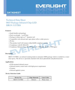
1. Product Overview
This document details the specifications for a high-performance, miniature surface-mount infrared (IR) emitting diode. The device is housed in a compact 0603 package, making it suitable for space-constrained applications requiring reliable infrared emission. Its primary function is to emit light in the near-infrared spectrum, with a typical peak wavelength of 870 nanometers (nm), which is optimally matched to the spectral sensitivity of silicon photodiodes and phototransistors. The core material is AlGaAs (Aluminum Gallium Arsenide), known for its efficient infrared light generation.
1.1 Core Advantages and Target Market
The device offers several key advantages for modern electronic design. Its miniature double-ended SMD package allows for high-density PCB mounting and is compatible with automated pick-and-place assembly processes. It is designed to be compatible with both infrared and vapor phase reflow soldering, facilitating modern manufacturing workflows. The product is compliant with major environmental and safety standards, including RoHS (Restriction of Hazardous Substances), EU REACH regulations, and is Halogen-Free (Br <900 ppm, Cl <900 ppm, Br+Cl < 1500 ppm). This combination of small size, performance, and compliance makes it ideal for consumer electronics, industrial sensors, and communication devices.
Primary Applications Include:
- PCB-mounted infrared proximity and presence sensors.
- Infrared remote control units where higher radiant intensity is required.
- Barcode scanners and optical encoders.
- Various infrared-based data transmission and sensing systems.
2. In-Depth Technical Parameter Analysis
A thorough understanding of the electrical and optical parameters is crucial for reliable circuit design and ensuring the LED operates within its safe operating area (SOA).
2.1 Absolute Maximum Ratings
These ratings define the limits beyond which permanent damage to the device may occur. They are not intended for normal operation.
- Continuous Forward Current (IF): 65 mA. Exceeding this current, even momentarily, can cause catastrophic failure due to overheating of the semiconductor junction.
- Reverse Voltage (VR): 5 V. The LED has a low reverse breakdown voltage. Circuit designs must ensure the LED is not subjected to reverse bias exceeding this value, often requiring protection in AC or bidirectional signal environments.
- Power Dissipation (Pc): 110 mW at 25°C. This is the maximum power the package can dissipate as heat. The actual permissible power decreases as ambient temperature (Ta) increases. Derating is necessary for high-temperature applications.
- Temperature Ranges: Operating: -25°C to +85°C; Storage: -40°C to +100°C.
- Soldering Temperature (Tsol): 260°C for a maximum of 5 seconds. This defines the reflow soldering profile constraints.
2.2 Electro-Optical Characteristics (Ta=25°C)
These are the typical performance parameters under specified test conditions. Designers should use the typical or maximum/minimum values as appropriate for their design margins.
- Radiant Intensity (IE): 1.3 mW/sr (typical) at IF=20mA. Radiant intensity measures the optical power emitted per unit solid angle (steradian). It is a key parameter for determining the signal strength at a receiver. The minimum specified value is 1.0 mW/sr.
- Peak Wavelength (λp): 870 nm (typical), with a range from 860 nm to 900 nm. This is the wavelength at which the emission spectrum is strongest. Matching this to the peak sensitivity of the receiver (e.g., a silicon photodetector at ~850-950nm) maximizes system efficiency.
- Spectral Bandwidth (Δλ): 45 nm (typical). This is the full width at half maximum (FWHM) of the emission spectrum, indicating the range of wavelengths emitted.
- Forward Voltage (VF): 1.35 V (typical) at IF=20mA, ranging from 1.20 V to 1.70 V. This parameter is essential for calculating the current-limiting resistor value: R = (Vsupply - VF) / IF. The variation must be accounted for in robust designs.
- Reverse Current (IR): 10 µA (maximum) at VR=5V.
- Viewing Angle (2θ1/2): 140 degrees. This is the full angle where the radiant intensity drops to half of its peak value (on-axis). A wide viewing angle is beneficial for applications requiring broad coverage, such as proximity sensors.
3. Performance Curve Analysis
The provided characteristic curves offer valuable insights into the device's behavior under varying conditions, which is critical for real-world application design.
3.1 Forward Current vs. Ambient Temperature
This curve illustrates the relationship between the maximum permissible continuous forward current and the ambient temperature. It demonstrates the necessary derating of the forward current as temperature increases to stay within the power dissipation limit. At temperatures approaching the maximum operating temperature (+85°C), the allowable continuous current is significantly lower than the 65mA absolute maximum rating at 25°C.
3.2 Spectral Distribution
The spectral distribution graph shows the relative radiant power output as a function of wavelength. It confirms the peak wavelength (λp) of 870nm and the typical spectral bandwidth (Δλ) of approximately 45nm. The shape of this curve is important for filtering and for ensuring compatibility with the receiver's spectral response.
3.3 Peak Emission Wavelength vs. Ambient Temperature
This curve shows that the peak wavelength has a positive temperature coefficient, meaning it increases slightly with increasing junction temperature. This shift (typically around 0.1-0.3 nm/°C for AlGaAs devices) is important for precision sensing applications where wavelength stability is critical.
3.4 Forward Voltage vs. Ambient Temperature
The forward voltage (VF) has a negative temperature coefficient; it decreases as temperature increases. This characteristic must be considered in constant-current drive circuits, as a lower VF at high temperature could slightly affect the power dissipation calculation if using a simple series resistor.
3.5 Relative Radiant Intensity vs. Angular Displacement
This polar plot visually defines the viewing angle (140° at half-intensity points). The radiation pattern is typically Lambertian or near-Lambertian for this package style, which is useful for modeling the irradiance on a target surface at various angles and distances.
4. Mechanical and Packaging Information
4.1 Package Dimensions (0603)
The device conforms to the standard 0603 (1608 metric) footprint: approximately 1.6mm in length, 0.8mm in width, and 0.8mm in height. Detailed dimensional drawings specify pad layout, component outline, and terminal positions with a standard tolerance of ±0.1mm unless otherwise noted. Correct land pattern design is essential for reliable soldering and mechanical stability.
4.2 Polarity Identification
The datasheet includes a diagram indicating the anode and cathode terminals. Correct polarity is mandatory for device operation. Typically, the cathode may be marked by a notch, a green indicator, or a specific pad shape on the tape and reel packaging.
4.3 Tape and Reel Specifications
The product is supplied in 8mm wide embossed carrier tape on 7-inch diameter reels. The carrier tape dimensions are specified to ensure compatibility with standard SMD assembly equipment. Each reel contains 4000 pieces.
5. Soldering and Assembly Guidelines
Proper handling is critical to maintain device reliability and performance.
5.1 Moisture Sensitivity and Storage
The device is moisture-sensitive (MSL). Precautions include:
- Do not open the moisture-proof barrier bag until ready for use.
- Store unopened bags at ≤30°C and ≤90% RH.
- Use within one year of shipment.
- After opening, store at ≤30°C and ≤60% RH.
- Use within 168 hours (7 days) after opening the bag.
- If the storage time is exceeded or the desiccant indicates moisture ingress, bake at 60 ±5°C for a minimum of 24 hours before use.
5.2 Reflow Soldering Profile
A Pb-free reflow soldering profile is recommended. Key parameters include a peak temperature of 260°C, with the time above 240°C not exceeding the recommended limit (implied by the 5-second maximum at 260°C). Reflow soldering should not be performed more than two times to avoid excessive thermal stress on the epoxy package and wire bonds.
5.3 Hand Soldering and Rework
If hand soldering is necessary, use a soldering iron with a tip temperature below 350°C and apply heat to each terminal for no more than 3 seconds. Use a low-power iron (≤25W). Allow a cooling interval of more than 2 seconds between soldering each terminal. For rework, a dual-head soldering iron is recommended to simultaneously heat both terminals and avoid mechanical stress. The feasibility and impact of rework on device characteristics should be verified beforehand.
6. Application Design Considerations
6.1 Current Limiting is Mandatory
An LED is a current-driven device. A series current-limiting resistor is absolutely required. The forward voltage (VF) has a narrow range, and a small increase in applied voltage beyond VF causes a large, potentially destructive increase in forward current (IF). The resistor value is calculated based on the supply voltage (Vsupply), the desired forward current (IF), and the forward voltage (VF), using the worst-case VF (minimum) to ensure current does not exceed the design maximum.
6.2 Thermal Management
While the package is small, power dissipation (up to 110mW) generates heat. For continuous operation at high currents or in elevated ambient temperatures, consider the thermal resistance of the PCB. Providing adequate copper area (thermal relief pads) around the solder pads helps dissipate heat and maintain a lower junction temperature, which improves long-term reliability and prevents luminous output degradation.
6.3 Optical Design
The 140-degree viewing angle provides broad emission. For applications requiring a more focused beam, external lenses or reflectors can be used. Conversely, for very wide-area coverage, the native angle may be sufficient. The water-clear lens is suitable for applications where the exact emission point is not critical; if a specific color or diffusion is needed for assembly alignment, this must be considered as the lens does not provide it.
6.4 Circuit Protection
In environments where reverse voltage transients are possible (e.g., inductive loads, hot-plugging), consider adding a protection diode in parallel with the LED (cathode to anode) to clamp any reverse voltage below the 5V maximum rating.
7. Comparison and Selection Guidance
This device is part of a family of IR LEDs. The key selection criteria from the provided guide is the chip material (AlGaAs) and lens color (Water Clear). When selecting an IR LED, engineers must compare key parameters:
- Wavelength (λp): Match to the peak sensitivity of the receiver (photodiode, phototransistor, or IC). 870nm is a common standard.
- Radiant Intensity (IE): Higher intensity provides a stronger signal, allowing for longer range or lower drive current.
- Viewing Angle: A narrow angle provides longer range and more focused light; a wide angle provides broader coverage.
- Package Size: The 0603 package offers a very small footprint for miniaturized designs.
- Forward Voltage: Lower VF can be advantageous in low-voltage battery-operated circuits.
The primary differentiator of this specific part is its combination of a standard 0603 footprint with a relatively high radiant intensity and wide viewing angle, suitable for general-purpose IR sensing and communication.
8. Frequently Asked Questions (Based on Technical Parameters)
8.1 What is the purpose of the 870nm wavelength?
870nm is in the near-infrared spectrum, invisible to the human eye. It is efficiently detected by inexpensive and common silicon-based photodetectors, which have peak sensitivity around 800-950nm. This makes it ideal for sensing, remote control, and optical isolation applications.
8.2 Can I drive this LED directly from a 3.3V or 5V microcontroller pin?
No. You must use a current-limiting resistor. For example, to drive at IF=20mA from a 3.3V supply, assuming a typical VF of 1.35V: R = (3.3V - 1.35V) / 0.020A = 97.5Ω. Use a standard 100Ω resistor. Always verify the current does not exceed the maximum under worst-case VF conditions.
8.3 How does temperature affect performance?
As temperature increases: Radiant output typically decreases, forward voltage decreases, and peak wavelength increases slightly. For stable operation, design drive circuitry that accounts for these variations, especially if operating over the full -25°C to +85°C range.
8.4 Is a heat sink required?
For continuous operation at the absolute maximum current (65mA) at room temperature, the power dissipation is P = VF * IF ≈ 1.35V * 0.065A ≈ 88mW, which is below the 110mW rating. However, at high ambient temperatures, derating is necessary. Good PCB thermal design (copper pads) usually suffices; a separate heat sink is not typical for 0603 packages.
9. Practical Application Example: Simple IR Proximity Sensor
A common use case is a reflective object sensor. The IR LED is placed adjacent to a phototransistor. A microcontroller pulses the LED (e.g., at 20mA). The light reflects off a nearby object and is detected by the phototransistor, whose output is read by the microcontroller. Design steps:
- LED Drive: Use a GPIO pin and an NPN transistor (or a MOSFET) with a series resistor to pulse the LED at the desired current. Pulsing allows for higher instantaneous current (for stronger signal) while keeping average power low.
- Receiver Circuit: The phototransistor is connected in a common-emitter configuration with a pull-up resistor to create a voltage output. The value of the collector resistor determines sensitivity and response speed.
- Optical Considerations: A small barrier between the LED and phototransistor on the PCB helps reduce direct crosstalk. The wide 140° viewing angle of the LED helps illuminate a broad area in front of the sensor.
- Signal Processing: The microcontroller can use synchronous detection (only reading the receiver during the LED pulse) to reject ambient light interference.
10. Operating Principle and Technology Trends
10.1 Basic Operating Principle
An infrared LED is a semiconductor p-n junction diode. When forward biased, electrons from the n-region recombine with holes from the p-region in the active region (made of AlGaAs). This recombination process releases energy in the form of photons (light). The specific bandgap energy of the AlGaAs material determines the wavelength of the emitted photons, which in this case is in the 870nm infrared range. The water-clear epoxy package encapsulates the chip, provides mechanical protection, and acts as a lens shaping the emission pattern.
10.2 Industry Trends
The trend in SMD infrared LEDs continues toward higher efficiency (more radiant output per unit electrical input), smaller package sizes for greater design flexibility, and increased integration. This includes devices with built-in drivers, modulated output for improved noise immunity, and multi-chip packages combining different wavelengths or combining an emitter and detector in a single package. There is also a strong focus on improving high-temperature performance and reliability for automotive and industrial applications. The device described here represents a mature, reliable, and widely adopted solution within this evolving landscape.
LED Specification Terminology
Complete explanation of LED technical terms
Photoelectric Performance
| Term | Unit/Representation | Simple Explanation | Why Important |
|---|---|---|---|
| Luminous Efficacy | lm/W (lumens per watt) | Light output per watt of electricity, higher means more energy efficient. | Directly determines energy efficiency grade and electricity cost. |
| Luminous Flux | lm (lumens) | Total light emitted by source, commonly called "brightness". | Determines if the light is bright enough. |
| Viewing Angle | ° (degrees), e.g., 120° | Angle where light intensity drops to half, determines beam width. | Affects illumination range and uniformity. |
| CCT (Color Temperature) | K (Kelvin), e.g., 2700K/6500K | Warmth/coolness of light, lower values yellowish/warm, higher whitish/cool. | Determines lighting atmosphere and suitable scenarios. |
| CRI / Ra | Unitless, 0–100 | Ability to render object colors accurately, Ra≥80 is good. | Affects color authenticity, used in high-demand places like malls, museums. |
| SDCM | MacAdam ellipse steps, e.g., "5-step" | Color consistency metric, smaller steps mean more consistent color. | Ensures uniform color across same batch of LEDs. |
| Dominant Wavelength | nm (nanometers), e.g., 620nm (red) | Wavelength corresponding to color of colored LEDs. | Determines hue of red, yellow, green monochrome LEDs. |
| Spectral Distribution | Wavelength vs intensity curve | Shows intensity distribution across wavelengths. | Affects color rendering and quality. |
Electrical Parameters
| Term | Symbol | Simple Explanation | Design Considerations |
|---|---|---|---|
| Forward Voltage | Vf | Minimum voltage to turn on LED, like "starting threshold". | Driver voltage must be ≥Vf, voltages add up for series LEDs. |
| Forward Current | If | Current value for normal LED operation. | Usually constant current drive, current determines brightness & lifespan. |
| Max Pulse Current | Ifp | Peak current tolerable for short periods, used for dimming or flashing. | Pulse width & duty cycle must be strictly controlled to avoid damage. |
| Reverse Voltage | Vr | Max reverse voltage LED can withstand, beyond may cause breakdown. | Circuit must prevent reverse connection or voltage spikes. |
| Thermal Resistance | Rth (°C/W) | Resistance to heat transfer from chip to solder, lower is better. | High thermal resistance requires stronger heat dissipation. |
| ESD Immunity | V (HBM), e.g., 1000V | Ability to withstand electrostatic discharge, higher means less vulnerable. | Anti-static measures needed in production, especially for sensitive LEDs. |
Thermal Management & Reliability
| Term | Key Metric | Simple Explanation | Impact |
|---|---|---|---|
| Junction Temperature | Tj (°C) | Actual operating temperature inside LED chip. | Every 10°C reduction may double lifespan; too high causes light decay, color shift. |
| Lumen Depreciation | L70 / L80 (hours) | Time for brightness to drop to 70% or 80% of initial. | Directly defines LED "service life". |
| Lumen Maintenance | % (e.g., 70%) | Percentage of brightness retained after time. | Indicates brightness retention over long-term use. |
| Color Shift | Δu′v′ or MacAdam ellipse | Degree of color change during use. | Affects color consistency in lighting scenes. |
| Thermal Aging | Material degradation | Deterioration due to long-term high temperature. | May cause brightness drop, color change, or open-circuit failure. |
Packaging & Materials
| Term | Common Types | Simple Explanation | Features & Applications |
|---|---|---|---|
| Package Type | EMC, PPA, Ceramic | Housing material protecting chip, providing optical/thermal interface. | EMC: good heat resistance, low cost; Ceramic: better heat dissipation, longer life. |
| Chip Structure | Front, Flip Chip | Chip electrode arrangement. | Flip chip: better heat dissipation, higher efficacy, for high-power. |
| Phosphor Coating | YAG, Silicate, Nitride | Covers blue chip, converts some to yellow/red, mixes to white. | Different phosphors affect efficacy, CCT, and CRI. |
| Lens/Optics | Flat, Microlens, TIR | Optical structure on surface controlling light distribution. | Determines viewing angle and light distribution curve. |
Quality Control & Binning
| Term | Binning Content | Simple Explanation | Purpose |
|---|---|---|---|
| Luminous Flux Bin | Code e.g., 2G, 2H | Grouped by brightness, each group has min/max lumen values. | Ensures uniform brightness in same batch. |
| Voltage Bin | Code e.g., 6W, 6X | Grouped by forward voltage range. | Facilitates driver matching, improves system efficiency. |
| Color Bin | 5-step MacAdam ellipse | Grouped by color coordinates, ensuring tight range. | Guarantees color consistency, avoids uneven color within fixture. |
| CCT Bin | 2700K, 3000K etc. | Grouped by CCT, each has corresponding coordinate range. | Meets different scene CCT requirements. |
Testing & Certification
| Term | Standard/Test | Simple Explanation | Significance |
|---|---|---|---|
| LM-80 | Lumen maintenance test | Long-term lighting at constant temperature, recording brightness decay. | Used to estimate LED life (with TM-21). |
| TM-21 | Life estimation standard | Estimates life under actual conditions based on LM-80 data. | Provides scientific life prediction. |
| IESNA | Illuminating Engineering Society | Covers optical, electrical, thermal test methods. | Industry-recognized test basis. |
| RoHS / REACH | Environmental certification | Ensures no harmful substances (lead, mercury). | Market access requirement internationally. |
| ENERGY STAR / DLC | Energy efficiency certification | Energy efficiency and performance certification for lighting. | Used in government procurement, subsidy programs, enhances competitiveness. |