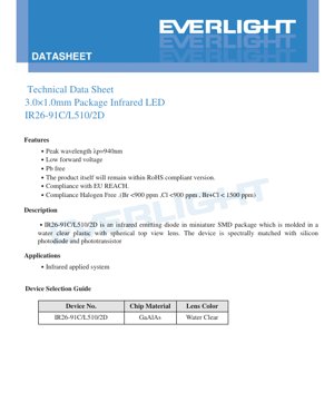
1. Product Overview
The IR26-91C/L510/2D is a miniature surface-mount device (SMD) infrared emitting diode. It is housed in a compact 3.0mm x 1.0mm package molded from water-clear plastic with a spherical top-view lens. The primary function of this component is to emit infrared light with a peak wavelength of 940 nanometers (nm), which is spectrally matched to the sensitivity of common silicon photodiodes and phototransistors. This makes it an ideal source for infrared sensing and communication systems where precise optical coupling is required.
1.1 Core Features and Advantages
The device offers several key technical and compliance advantages. Its primary optical feature is the 940nm peak wavelength, chosen for optimal performance with silicon-based detectors while offering good atmospheric transmission. Electrically, it boasts a low typical forward voltage of 1.3V at 20mA, contributing to energy-efficient operation. The component is manufactured to be lead-free (Pb-free) and complies with the European Union's Restriction of Hazardous Substances (RoHS) directive and the Registration, Evaluation, Authorisation and Restriction of Chemicals (REACH) regulation. It is also classified as halogen-free, with bromine (Br) and chlorine (Cl) content each below 900 parts per million (ppm) and their combined total below 1500 ppm.
1.2 Target Applications
This infrared LED is designed for use in various infrared-applied systems. Typical applications include proximity sensors, object detection, touchless switches, optical encoders, and short-range data transmission links. Its small form factor and SMD design make it suitable for automated assembly processes in consumer electronics, industrial automation, and automotive interior sensing modules.
2. Technical Parameter Analysis
This section provides a detailed, objective interpretation of the key electrical, optical, and thermal parameters specified in the datasheet. Understanding these ratings is critical for reliable circuit design and ensuring the long-term performance of the device.
2.1 Absolute Maximum Ratings
The Absolute Maximum Ratings define the stress limits beyond which permanent damage to the device may occur. These ratings are not for continuous operation. The continuous forward current (IF) is rated at 65 mA. A significantly higher peak forward current (IFP) of 700 mA is permissible, but only under strict pulsed conditions: pulse width ≤ 70 microseconds (μs) and duty cycle ≤ 0.7%. The maximum reverse voltage (VR) is 5V, indicating the LED has a very low tolerance for reverse bias. The device can operate in ambient temperatures (Topr) from -40°C to +85°C and be stored (Tstg) from -40°C to +100°C. The maximum soldering temperature (Tsol) during reflow is 260°C for a duration not exceeding 5 seconds. The power dissipation (Pd) at or below 25°C free air temperature is 100 mW. It also features Electrostatic Discharge (ESD) protection, with a Human Body Model (HBM) rating of a minimum 2000V and a Machine Model (MM) rating of a minimum 200V.
2.2 Electro-Optical Characteristics
The Electro-Optical Characteristics table provides typical and maximum/minimum values under specified test conditions (Ta=25°C). The radiant intensity (Ie), a measure of optical power per solid angle, is typically 8.0 milliwatts per steradian (mW/sr) at a forward current of 20mA. The peak wavelength (λp) is centered at 940nm. The spectral bandwidth (Δλ), representing the range of wavelengths emitted at half the peak intensity, is typically 45nm. The forward voltage (VF) ranges from a typical 1.3V to a maximum of 1.6V at 20mA. The reverse current (IR) has a maximum value of 10 microamperes (μA) when a 5V reverse bias is applied. The viewing angle, defined as the full angle where intensity drops to half its peak value, is asymmetrical: approximately 130 degrees in the X-axis and 20 degrees in the Y-axis. This creates a highly elliptical radiation pattern, which is a critical design consideration for beam shaping and sensor alignment.
3. Performance Curve Analysis
The datasheet includes several graphs that illustrate the device's behavior under varying conditions. These curves are essential for understanding non-linear relationships and designing for different operating environments.
3.1 Forward Current vs. Ambient Temperature
This derating curve shows how the maximum allowable continuous forward current decreases as the ambient temperature increases. At 25°C, the full 65mA rating is available. As temperature rises, the current must be reduced to prevent exceeding the maximum junction temperature and power dissipation limits, ensuring long-term reliability.
3.2 Spectral Distribution
The spectral distribution plot graphically represents the light output as a function of wavelength. It confirms the peak at 940nm and the approximately 45nm spectral bandwidth (Full Width at Half Maximum - FWHM). The curve shows that very little visible light (below ~700nm) is emitted, which is desirable for discreet operation in IR systems.
3.3 Radiant Intensity vs. Forward Current
This curve demonstrates the relationship between the drive current and the optical output power. It is generally linear at lower currents but may exhibit saturation or reduced efficiency at very high currents due to thermal effects. Designers use this to determine the required drive current to achieve a specific signal level at the detector.
3.4 Angular Radiation Patterns
Separate plots for the X-axis and Y-axis show the relative radiant intensity as a function of angular displacement from the optical center (0°). The X-axis pattern is very wide (~130° half-angle), while the Y-axis pattern is much narrower (~20° half-angle). This elliptical pattern must be accounted for when aligning the LED with a sensor or designing optical elements like lenses or apertures.
4. Mechanical and Packaging Information
4.1 Package Dimensions and Tolerances
The device has a nominal package size of 3.0mm in length, 1.0mm in width, and a specified height. A detailed dimensional drawing is provided, including pad locations, lens shape, and polarity indicator (typically a notch or a dot on the cathode side). All unspecified dimensions have a tolerance of ±0.1mm. A recommended soldering pad pattern for side-view mounting is also illustrated to ensure proper mechanical stability and solder joint formation during reflow.
4.2 Carrier Tape and Reel Packaging
For automated pick-and-place assembly, the LEDs are supplied in embossed carrier tape wound onto reels. The datasheet provides the precise dimensions of the carrier tape pockets, pitch, and reel specifications. A standard reel contains 2000 pieces. This information is vital for configuring assembly equipment feeders correctly.
5. Soldering and Assembly Guidelines
Proper handling and soldering are crucial to prevent damage to the LED and ensure solder joint reliability.
5.1 Reflow Soldering Profile
The component is suitable for lead-free (Pb-free) reflow soldering processes. A recommended temperature profile is provided, typically including preheat, soak, reflow (peak temperature ≤ 260°C for ≤ 5 seconds), and cooling stages. The number of reflow cycles should not exceed three to minimize thermal stress on the plastic package and internal wire bonds.
5.2 Hand Soldering and Rework
If hand soldering is necessary, extreme care must be taken. The soldering iron tip temperature should be below 350°C, and contact time per terminal should be limited to 3 seconds or less. A low-power iron (≤25W) is recommended. For rework, a double-head soldering iron is suggested to simultaneously heat both terminals and avoid mechanical stress on the solder joints. The feasibility and impact of rework should be evaluated beforehand.
5.3 Moisture Sensitivity and Storage
The SMD package is moisture-sensitive. The device must be stored in its original moisture-proof bag with desiccant at ≤30°C and ≤90% relative humidity (RH). The shelf life before the bag is opened is one year. After opening, the components should be stored at ≤30°C and ≤70% RH and used within 168 hours (7 days). If these conditions are exceeded or the desiccant indicates saturation, a baking treatment at 60 ±5°C for a minimum of 24 hours is required before use to remove absorbed moisture and prevent \"popcorning\" during reflow.
6. Application Design Considerations
6.1 Drive Circuit Design
A critical design note is the need for current limiting. The LED must be driven with a current source or, more commonly, a voltage source in series with a current-limiting resistor. The datasheet explicitly warns that a slight voltage shift can cause a large current change, potentially leading to burnout. The resistor value (Rlimit) can be calculated using Ohm's Law: Rlimit = (Vsupply - VF) / IF, where VF is the forward voltage of the LED at the desired current IF. Using the maximum VF (1.6V) for this calculation ensures the current does not exceed the target under all conditions.
6.2 Optical Design and Alignment
Due to the highly elliptical beam pattern (130° x 20°), careful optical design is necessary. For applications requiring a circular spot or specific illumination profile, secondary optics such as lenses or reflectors may be needed. The alignment between the LED and the paired photodetector is also more critical along the narrow Y-axis. Designers should consult the angular displacement graphs to understand the intensity fall-off.
6.3 Thermal Management
While the power dissipation is relatively low (100mW max), effective thermal management is still important, especially in high ambient temperature environments or when driving at high currents. The derating curve must be followed. Ensuring adequate copper area on the PCB under and around the LED pads helps dissipate heat and maintain lower junction temperatures, which preserves luminous efficiency and longevity.
7. Technical Comparison and Differentiation
The IR26-91C/L510/2D differentiates itself in the market through a specific combination of parameters. Its 940nm wavelength is a common standard, offering a good balance between silicon detector sensitivity and lower ambient light interference compared to 850nm LEDs. The very low forward voltage (1.3V typical) is a key advantage for battery-powered or low-voltage logic circuits, as it reduces the voltage headroom required for the driver. The compact 3.0x1.0mm footprint allows for high-density PCB layouts. The compliance with RoHS, REACH, and halogen-free standards makes it suitable for global markets with strict environmental regulations. The asymmetrical viewing angle can be either an advantage or a constraint, depending on the application's optical requirements.
8. Frequently Asked Questions (FAQ)
8.1 Why is a current-limiting resistor mandatory?
An LED is a diode with a non-linear current-voltage (I-V) characteristic. Beyond its turn-on voltage, a small increase in voltage causes a very large increase in current. Operating directly from a voltage source without a series resistor would allow the current to rise uncontrollably, quickly exceeding the Absolute Maximum Rating and destroying the device. The resistor provides a linear, predictable relationship between supply voltage and LED current.
8.2 Can I drive this LED with a 3.3V or 5V microcontroller pin?
Yes, but a series resistor is always required. For example, to drive at IF=20mA from a 3.3V supply, assuming VF=1.5V: R = (3.3V - 1.5V) / 0.020A = 90 Ohms. A standard 91 Ohm resistor would be suitable. The microcontroller pin must also be capable of sourcing or sinking the required 20mA current.
8.3 What is the purpose of the 940nm wavelength?
940nm infrared light is invisible to the human eye, allowing for discreet operation. It is strongly absorbed by silicon, the material used in most photodiodes and phototransistors, making detection efficient. It also experiences less interference from common ambient light sources (which have less IR content at 940nm compared to 850nm) and is less susceptible to noise in imaging sensors.
8.4 How do I identify the anode and cathode?
The package includes a polarity marker. Consult the package dimension drawing in the datasheet. It is common for the cathode to be marked by a green dot, a notch in the package, or a chamfered corner. Incorrect polarity connection will prevent the LED from emitting light and, if a reverse voltage exceeding 5V is applied, may damage the device.
9. Practical Design Case Study
Consider designing a simple object detection sensor using this LED and a silicon phototransistor. The LED is driven by a 5V supply through a 180 Ohm resistor (limiting current to ~20mA, assuming VF=1.5V). The phototransistor is placed a few centimeters away, aligned on the same optical axis. When no object is present, the IR light from the LED does not reach the phototransistor, and its output is low. When an object passes between them, it reflects some of the IR light onto the phototransistor, causing its output current to increase. This signal can be amplified and fed into a comparator or microcontroller ADC to detect the object's presence. The elliptical beam pattern of the LED means the sensor's effective detection zone will be wider horizontally than vertically, which must be considered when defining the sensor's field of view.
10. Operating Principle
An Infrared Light Emitting Diode (IR LED) operates on the principle of electroluminescence in a semiconductor material. The IR26-91C/L510/2D uses a Gallium Aluminum Arsenide (GaAlAs) chip. When a forward voltage exceeding the diode's bandgap voltage is applied, electrons from the n-type region are injected across the p-n junction into the p-type region, and holes are injected in the opposite direction. These charge carriers (electrons and holes) recombine in the active region of the junction. The energy released during this recombination is emitted as photons (light particles). The specific composition of the GaAlAs semiconductor determines the bandgap energy, which directly dictates the wavelength of the emitted photons—in this case, centered around 940nm in the infrared spectrum.
11. Industry Trends
The market for infrared LEDs continues to evolve. Key trends include the push for higher radiant intensity and efficiency from smaller packages to enable more powerful sensing in compact devices. There is growing integration of IR LEDs with drivers and sensors into complete modules or systems-in-package (SiP). The demand for specific wavelengths is diversifying; while 940nm remains standard, wavelengths like 850nm (for surveillance) and 1050nm/1300nm (for specific sensing applications) are gaining traction. Furthermore, the drive for lower power consumption and improved reliability in automotive (e.g., in-cabin monitoring), consumer (e.g., face ID), and industrial IoT applications is pushing advancements in chip technology, packaging, and thermal management for IR emitters.
LED Specification Terminology
Complete explanation of LED technical terms
Photoelectric Performance
| Term | Unit/Representation | Simple Explanation | Why Important |
|---|---|---|---|
| Luminous Efficacy | lm/W (lumens per watt) | Light output per watt of electricity, higher means more energy efficient. | Directly determines energy efficiency grade and electricity cost. |
| Luminous Flux | lm (lumens) | Total light emitted by source, commonly called "brightness". | Determines if the light is bright enough. |
| Viewing Angle | ° (degrees), e.g., 120° | Angle where light intensity drops to half, determines beam width. | Affects illumination range and uniformity. |
| CCT (Color Temperature) | K (Kelvin), e.g., 2700K/6500K | Warmth/coolness of light, lower values yellowish/warm, higher whitish/cool. | Determines lighting atmosphere and suitable scenarios. |
| CRI / Ra | Unitless, 0–100 | Ability to render object colors accurately, Ra≥80 is good. | Affects color authenticity, used in high-demand places like malls, museums. |
| SDCM | MacAdam ellipse steps, e.g., "5-step" | Color consistency metric, smaller steps mean more consistent color. | Ensures uniform color across same batch of LEDs. |
| Dominant Wavelength | nm (nanometers), e.g., 620nm (red) | Wavelength corresponding to color of colored LEDs. | Determines hue of red, yellow, green monochrome LEDs. |
| Spectral Distribution | Wavelength vs intensity curve | Shows intensity distribution across wavelengths. | Affects color rendering and quality. |
Electrical Parameters
| Term | Symbol | Simple Explanation | Design Considerations |
|---|---|---|---|
| Forward Voltage | Vf | Minimum voltage to turn on LED, like "starting threshold". | Driver voltage must be ≥Vf, voltages add up for series LEDs. |
| Forward Current | If | Current value for normal LED operation. | Usually constant current drive, current determines brightness & lifespan. |
| Max Pulse Current | Ifp | Peak current tolerable for short periods, used for dimming or flashing. | Pulse width & duty cycle must be strictly controlled to avoid damage. |
| Reverse Voltage | Vr | Max reverse voltage LED can withstand, beyond may cause breakdown. | Circuit must prevent reverse connection or voltage spikes. |
| Thermal Resistance | Rth (°C/W) | Resistance to heat transfer from chip to solder, lower is better. | High thermal resistance requires stronger heat dissipation. |
| ESD Immunity | V (HBM), e.g., 1000V | Ability to withstand electrostatic discharge, higher means less vulnerable. | Anti-static measures needed in production, especially for sensitive LEDs. |
Thermal Management & Reliability
| Term | Key Metric | Simple Explanation | Impact |
|---|---|---|---|
| Junction Temperature | Tj (°C) | Actual operating temperature inside LED chip. | Every 10°C reduction may double lifespan; too high causes light decay, color shift. |
| Lumen Depreciation | L70 / L80 (hours) | Time for brightness to drop to 70% or 80% of initial. | Directly defines LED "service life". |
| Lumen Maintenance | % (e.g., 70%) | Percentage of brightness retained after time. | Indicates brightness retention over long-term use. |
| Color Shift | Δu′v′ or MacAdam ellipse | Degree of color change during use. | Affects color consistency in lighting scenes. |
| Thermal Aging | Material degradation | Deterioration due to long-term high temperature. | May cause brightness drop, color change, or open-circuit failure. |
Packaging & Materials
| Term | Common Types | Simple Explanation | Features & Applications |
|---|---|---|---|
| Package Type | EMC, PPA, Ceramic | Housing material protecting chip, providing optical/thermal interface. | EMC: good heat resistance, low cost; Ceramic: better heat dissipation, longer life. |
| Chip Structure | Front, Flip Chip | Chip electrode arrangement. | Flip chip: better heat dissipation, higher efficacy, for high-power. |
| Phosphor Coating | YAG, Silicate, Nitride | Covers blue chip, converts some to yellow/red, mixes to white. | Different phosphors affect efficacy, CCT, and CRI. |
| Lens/Optics | Flat, Microlens, TIR | Optical structure on surface controlling light distribution. | Determines viewing angle and light distribution curve. |
Quality Control & Binning
| Term | Binning Content | Simple Explanation | Purpose |
|---|---|---|---|
| Luminous Flux Bin | Code e.g., 2G, 2H | Grouped by brightness, each group has min/max lumen values. | Ensures uniform brightness in same batch. |
| Voltage Bin | Code e.g., 6W, 6X | Grouped by forward voltage range. | Facilitates driver matching, improves system efficiency. |
| Color Bin | 5-step MacAdam ellipse | Grouped by color coordinates, ensuring tight range. | Guarantees color consistency, avoids uneven color within fixture. |
| CCT Bin | 2700K, 3000K etc. | Grouped by CCT, each has corresponding coordinate range. | Meets different scene CCT requirements. |
Testing & Certification
| Term | Standard/Test | Simple Explanation | Significance |
|---|---|---|---|
| LM-80 | Lumen maintenance test | Long-term lighting at constant temperature, recording brightness decay. | Used to estimate LED life (with TM-21). |
| TM-21 | Life estimation standard | Estimates life under actual conditions based on LM-80 data. | Provides scientific life prediction. |
| IESNA | Illuminating Engineering Society | Covers optical, electrical, thermal test methods. | Industry-recognized test basis. |
| RoHS / REACH | Environmental certification | Ensures no harmful substances (lead, mercury). | Market access requirement internationally. |
| ENERGY STAR / DLC | Energy efficiency certification | Energy efficiency and performance certification for lighting. | Used in government procurement, subsidy programs, enhances competitiveness. |