Table of Contents
- 1. Product Overview
- 2. In-Depth Technical Parameter Analysis
- 2.1 Absolute Maximum Ratings
- 2.2 Electro-Optical Characteristics (Ta=25°C)
- 3. Performance Curve Analysis
- 3.1 Forward Current vs. Ambient Temperature
- 3.2 Spectral Distribution
- 3.3 Forward Current vs. Forward Voltage (I-V Curve)
- 3.4 Radiant Intensity vs. Forward Current
- 3.5 Relative Radiant Intensity vs. Angular Displacement
- 4. Mechanical and Packaging Information
- 4.1 Device Dimensions
- 4.2 Polarity Identification
- 4.3 Packaging Specifications
- 5. Soldering, Assembly, and Handling Guidelines
- 5.1 Critical Precautions
- 5.2 Soldering Process
- 6. Application Suggestions and Design Considerations
- 6.1 Typical Application Scenarios
- 6.2 Design Considerations
- 7. Technical Comparison and Differentiation
- 8. Frequently Asked Questions (FAQs)
- 8.1 What is the purpose of the "water clear" lens if it's an IR LED?
- 8.2 Can I drive this LED at its maximum current of 65mA continuously?
- 8.3 How do I identify the anode and cathode?
- 8.4 Why is the storage and handling so strict regarding moisture?
- 9. Operating Principle
- 10. Industry Trends
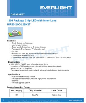
1. Product Overview
The HIR25-21C/L289/2T is a high-performance infrared (IR) emitting diode housed in a miniature 1206 surface-mount device (SMD) package. This component is specifically engineered for applications requiring reliable infrared emission matched to silicon-based photodetectors. Its core function is to convert electrical energy into infrared light at a peak wavelength of 850 nanometers (nm).
The device is constructed with a GaAlAs (Gallium Aluminum Arsenide) chip material, which is known for its efficiency in the infrared spectrum. The package is molded from water-clear plastic and incorporates a spherical inner lens. This lens design is crucial for controlling the light output pattern, resulting in a typical viewing angle (2θ1/2) of 60 degrees. The "water clear" appearance indicates the lens material does not filter visible light, allowing the maximum transmission of the intended infrared radiation.
A key advantage of this LED is its spectral matching to silicon photodiodes and phototransistors. Silicon detectors have peak sensitivity in the near-infrared region, and the 850nm output of this LED aligns well with this characteristic, ensuring optimal signal strength and system efficiency in sensing applications.
2. In-Depth Technical Parameter Analysis
2.1 Absolute Maximum Ratings
These ratings define the limits beyond which permanent damage to the device may occur. Operation under these conditions is not guaranteed.
- Continuous Forward Current (IF): 65 mA. This is the maximum DC current that can be continuously applied to the LED anode.
- Reverse Voltage (VR): 5 V. Applying a reverse voltage higher than this can break down the LED's PN junction.
- Power Dissipation (Pd): 130 mW at or below 25°C ambient temperature. This is the maximum power the package can dissipate as heat. Exceeding this limit risks overheating.
- Operating & Storage Temperature: -25°C to +85°C (operating), -40°C to +85°C (storage).
- Soldering Temperature (Tsol): 260°C for a maximum of 5 seconds. This is critical for lead-free (Pb-free) reflow soldering processes.
2.2 Electro-Optical Characteristics (Ta=25°C)
These parameters are measured under standard test conditions (20mA forward current, 25°C) and define the device's performance.
- Radiant Intensity (Ie): 4.0 mW/sr (Min), 5.0 mW/sr (Typ). This measures the optical power emitted per unit solid angle (steradian). It is a direct indicator of the LED's brightness in its primary direction.
- Peak Wavelength (λp): 850 nm (Typ). The wavelength at which the optical output power is greatest. This is in the near-infrared (NIR) spectrum, invisible to the human eye.
- Spectral Bandwidth (Δλ): 30 nm (Typ). The range of wavelengths emitted, typically measured at half the peak power (Full Width at Half Maximum - FWHM). A 30nm bandwidth is standard for an IR LED.
- Forward Voltage (VF): 1.4 V (Typ), 1.7 V (Max) at 20mA. The voltage drop across the LED when operating. This low voltage is characteristic of GaAlAs IR diodes and is important for calculating series resistor values and power consumption.
- Reverse Current (IR): 10 μA (Max) at VR=5V. The small leakage current that flows when the diode is reverse-biased.
- Viewing Angle (2θ1/2): 60° (Typ). The full angle where the radiant intensity drops to half of its maximum value. The spherical lens creates this moderately wide beam.
3. Performance Curve Analysis
The datasheet provides several characteristic curves essential for design engineers.
3.1 Forward Current vs. Ambient Temperature
This graph shows the derating of the maximum allowable forward current as the ambient temperature increases. As temperature rises, the LED's ability to dissipate heat decreases, so the maximum current must be reduced to stay within the 130mW power dissipation limit. Designers must consult this curve for high-temperature operation.
3.2 Spectral Distribution
This plot visualizes the light output as a function of wavelength, centered around the 850nm peak with the 30nm FWHM bandwidth. It confirms the spectral match with silicon detectors, which typically have high responsivity around 800-900nm.
3.3 Forward Current vs. Forward Voltage (I-V Curve)
This fundamental curve shows the exponential relationship between current and voltage for a diode. The "knee" voltage is around 1.2-1.3V. The curve is vital for designing the driving circuit, especially for calculating the current-limiting resistor: R = (Vsupply - VF) / IF.
3.4 Radiant Intensity vs. Forward Current
This graph demonstrates the linear relationship between drive current and optical output power (radiant intensity) within the operating range. It shows that increasing current proportionally increases light output, up to the thermal limits of the device.
3.5 Relative Radiant Intensity vs. Angular Displacement
This polar plot illustrates the radiation pattern or beam profile. It visually confirms the 60° viewing angle, showing how intensity decreases as the angle from the central axis (0°) increases. This is critical for designing optical systems, ensuring the receiver is within the LED's effective beam.
4. Mechanical and Packaging Information
4.1 Device Dimensions
The component follows the standard 1206 SMD footprint: approximately 3.2mm in length, 1.6mm in width, and 1.1mm in height. Detailed dimensional drawings in the datasheet specify all critical measurements including pad spacing (2.0mm typical), component height, and lens curvature with tolerances of ±0.1mm unless otherwise noted.
4.2 Polarity Identification
The cathode is typically marked, often by a notch, a green stripe, or a different pad size/shape on the tape and reel packaging. The datasheet drawing indicates the cathode side. Correct polarity is essential during assembly to prevent reverse bias damage.
4.3 Packaging Specifications
The LEDs are supplied on 8mm wide embossed carrier tape wound on 7-inch diameter reels. Each reel contains 2000 pieces. The carrier tape dimensions (pocket size, pitch, etc.) are provided for automated pick-and-place machine programming.
5. Soldering, Assembly, and Handling Guidelines
5.1 Critical Precautions
- Current Limiting is Mandatory: An external series resistor must always be used. The LED's low forward voltage and sharp I-V curve mean that a small increase in supply voltage can cause a large, destructive increase in current.
- Moisture Sensitivity: The plastic package is moisture-sensitive. Devices must be stored in their original moisture-proof bag under controlled conditions (10-30°C, ≤60% RH). Once opened, the "floor life" is 168 hours (7 days) under the same conditions. Exceeding this requires baking (e.g., 96 hours at 60°C) before reflow soldering to prevent "popcorning" or package cracking.
5.2 Soldering Process
- Reflow Soldering: A lead-free (Pb-free) temperature profile is recommended, with a peak temperature of 260°C for a maximum of 5 seconds. Reflow should not be performed more than two times.
- Hand Soldering: If necessary, use a soldering iron with a tip temperature below 350°C and a power rating under 25W. Contact time per terminal should be less than 3 seconds, with intervals between soldering each terminal. A double-head soldering iron is suggested for any repair work to minimize thermal stress.
- Stress Avoidance: Do not apply mechanical stress to the LED during heating or bend the PCB after soldering, as this can damage the internal connections or the package.
6. Application Suggestions and Design Considerations
6.1 Typical Application Scenarios
- PCB-Mounted Infrared Sensors: Used as the emitter in proximity sensors, object detection, and line-following robots.
- Infrared Remote Control Units: Suitable for high-power requirement remotes, providing longer range or stronger signal penetration.
- Scanners: Barcode scanners, document scanners, and other optical scanning systems.
- General Infrared Systems: Security systems (IR illumination for cameras), data transmission (IrDA), and industrial automation.
6.2 Design Considerations
- Driver Circuit: Always include a current-limiting resistor. Calculate resistor value and power rating based on the supply voltage and desired forward current (e.g., 20mA for typical specs). For pulsed operation (like remote controls), higher peak currents may be possible if the duty cycle is low, but average power must not exceed ratings.
- Optical Design: Consider the 60° viewing angle when aligning the emitter with a photodetector. For longer range, external lenses or reflectors can be used to collimate the beam. For wider coverage, the native angle may be sufficient.
- Thermal Management: Ensure adequate PCB copper area or thermal vias to dissipate heat, especially when driving near maximum current or in high ambient temperatures.
- Electrical Noise: In sensitive analog sensing applications, consider modulating the IR signal and using synchronous detection to reject ambient light and electrical noise.
7. Technical Comparison and Differentiation
Compared to standard visible-light SMD LEDs or older through-hole IR LEDs, the HIR25-21C/L289/2T offers several advantages:
- Size & Mounting: The 1206 SMD package enables high-density, automated PCB assembly, saving space and cost compared to through-hole parts.
- Optical Performance: The integrated spherical lens provides a consistent, controlled radiation pattern (60°), which is more reliable than LEDs without a lens or with a flat window.
- Spectral Precision: The 850nm peak wavelength is a standard optimized for silicon detectors, offering a good balance between detector responsivity and ambient light rejection (sunlight has less IR at 850nm compared to 940nm).
- Compliance: The product is Pb-free, compliant with RoHS, REACH, and halogen-free standards (Br <900ppm, Cl <900ppm, Br+Cl <1500ppm), meeting modern environmental regulations.
8. Frequently Asked Questions (FAQs)
8.1 What is the purpose of the "water clear" lens if it's an IR LED?
The "water clear" plastic is highly transparent across a broad spectrum, including visible light and near-infrared. Its primary function is to protect the semiconductor chip and to be molded into a specific shape (spherical lens) that controls the light output pattern. It does not filter the IR light; in fact, it allows maximum transmission of the 850nm wavelength.
8.2 Can I drive this LED at its maximum current of 65mA continuously?
You can only drive it at 65mA if you can guarantee the ambient temperature is low enough and the thermal design is sufficient to keep the junction temperature within safe limits, ensuring the 130mW power dissipation is not exceeded. At higher ambient temperatures, the maximum allowable current derates significantly. For reliable long-term operation, driving at the typical 20mA condition is recommended.
8.3 How do I identify the anode and cathode?
The datasheet package drawing indicates the cathode. On the physical tape and reel, the cathode side of the pocket is often marked. On the component itself, look for a subtle mark like a notch, a dot, or a green stripe. When in doubt, refer to the manufacturer's packaging label or datasheet.
8.4 Why is the storage and handling so strict regarding moisture?
The plastic molding compound can absorb moisture from the air. During the high-temperature reflow soldering process, this absorbed moisture rapidly turns to steam, creating high internal pressure. This can cause delamination inside the package, cracks in the plastic, or "popcorning," leading to immediate failure or reduced long-term reliability. The MSL (Moisture Sensitivity Level) precautions prevent this.
9. Operating Principle
This device is a light-emitting diode (LED). When a forward voltage exceeding its bandgap voltage (approximately 1.4V) is applied across the anode and cathode, electrons and holes are injected into the active region of the GaAlAs semiconductor chip. When these charge carriers recombine, they release energy in the form of photons (light particles). The specific composition of the GaAlAs material determines the energy of these photons, which corresponds to the infrared wavelength of 850nm. The spherical lens then shapes and directs this emitted light into a 60-degree beam.
10. Industry Trends
Infrared LEDs continue to evolve driven by several key trends. There is a growing demand for higher radiant intensity and efficiency in smaller packages to enable more compact and powerful sensors. Integration is another significant trend, with IR emitters being combined with drivers, photodetectors, and even microcontrollers into single modules or system-in-package (SiP) solutions. Furthermore, the expansion of applications in automotive (in-cabin monitoring, LiDAR), consumer electronics (face recognition, gesture control), and industrial IoT is pushing for devices with improved reliability, wider operating temperature ranges, and enhanced resistance to harsh environments. Compliance with stringent environmental and safety regulations remains a fundamental requirement for all electronic components.
LED Specification Terminology
Complete explanation of LED technical terms
Photoelectric Performance
| Term | Unit/Representation | Simple Explanation | Why Important |
|---|---|---|---|
| Luminous Efficacy | lm/W (lumens per watt) | Light output per watt of electricity, higher means more energy efficient. | Directly determines energy efficiency grade and electricity cost. |
| Luminous Flux | lm (lumens) | Total light emitted by source, commonly called "brightness". | Determines if the light is bright enough. |
| Viewing Angle | ° (degrees), e.g., 120° | Angle where light intensity drops to half, determines beam width. | Affects illumination range and uniformity. |
| CCT (Color Temperature) | K (Kelvin), e.g., 2700K/6500K | Warmth/coolness of light, lower values yellowish/warm, higher whitish/cool. | Determines lighting atmosphere and suitable scenarios. |
| CRI / Ra | Unitless, 0–100 | Ability to render object colors accurately, Ra≥80 is good. | Affects color authenticity, used in high-demand places like malls, museums. |
| SDCM | MacAdam ellipse steps, e.g., "5-step" | Color consistency metric, smaller steps mean more consistent color. | Ensures uniform color across same batch of LEDs. |
| Dominant Wavelength | nm (nanometers), e.g., 620nm (red) | Wavelength corresponding to color of colored LEDs. | Determines hue of red, yellow, green monochrome LEDs. |
| Spectral Distribution | Wavelength vs intensity curve | Shows intensity distribution across wavelengths. | Affects color rendering and quality. |
Electrical Parameters
| Term | Symbol | Simple Explanation | Design Considerations |
|---|---|---|---|
| Forward Voltage | Vf | Minimum voltage to turn on LED, like "starting threshold". | Driver voltage must be ≥Vf, voltages add up for series LEDs. |
| Forward Current | If | Current value for normal LED operation. | Usually constant current drive, current determines brightness & lifespan. |
| Max Pulse Current | Ifp | Peak current tolerable for short periods, used for dimming or flashing. | Pulse width & duty cycle must be strictly controlled to avoid damage. |
| Reverse Voltage | Vr | Max reverse voltage LED can withstand, beyond may cause breakdown. | Circuit must prevent reverse connection or voltage spikes. |
| Thermal Resistance | Rth (°C/W) | Resistance to heat transfer from chip to solder, lower is better. | High thermal resistance requires stronger heat dissipation. |
| ESD Immunity | V (HBM), e.g., 1000V | Ability to withstand electrostatic discharge, higher means less vulnerable. | Anti-static measures needed in production, especially for sensitive LEDs. |
Thermal Management & Reliability
| Term | Key Metric | Simple Explanation | Impact |
|---|---|---|---|
| Junction Temperature | Tj (°C) | Actual operating temperature inside LED chip. | Every 10°C reduction may double lifespan; too high causes light decay, color shift. |
| Lumen Depreciation | L70 / L80 (hours) | Time for brightness to drop to 70% or 80% of initial. | Directly defines LED "service life". |
| Lumen Maintenance | % (e.g., 70%) | Percentage of brightness retained after time. | Indicates brightness retention over long-term use. |
| Color Shift | Δu′v′ or MacAdam ellipse | Degree of color change during use. | Affects color consistency in lighting scenes. |
| Thermal Aging | Material degradation | Deterioration due to long-term high temperature. | May cause brightness drop, color change, or open-circuit failure. |
Packaging & Materials
| Term | Common Types | Simple Explanation | Features & Applications |
|---|---|---|---|
| Package Type | EMC, PPA, Ceramic | Housing material protecting chip, providing optical/thermal interface. | EMC: good heat resistance, low cost; Ceramic: better heat dissipation, longer life. |
| Chip Structure | Front, Flip Chip | Chip electrode arrangement. | Flip chip: better heat dissipation, higher efficacy, for high-power. |
| Phosphor Coating | YAG, Silicate, Nitride | Covers blue chip, converts some to yellow/red, mixes to white. | Different phosphors affect efficacy, CCT, and CRI. |
| Lens/Optics | Flat, Microlens, TIR | Optical structure on surface controlling light distribution. | Determines viewing angle and light distribution curve. |
Quality Control & Binning
| Term | Binning Content | Simple Explanation | Purpose |
|---|---|---|---|
| Luminous Flux Bin | Code e.g., 2G, 2H | Grouped by brightness, each group has min/max lumen values. | Ensures uniform brightness in same batch. |
| Voltage Bin | Code e.g., 6W, 6X | Grouped by forward voltage range. | Facilitates driver matching, improves system efficiency. |
| Color Bin | 5-step MacAdam ellipse | Grouped by color coordinates, ensuring tight range. | Guarantees color consistency, avoids uneven color within fixture. |
| CCT Bin | 2700K, 3000K etc. | Grouped by CCT, each has corresponding coordinate range. | Meets different scene CCT requirements. |
Testing & Certification
| Term | Standard/Test | Simple Explanation | Significance |
|---|---|---|---|
| LM-80 | Lumen maintenance test | Long-term lighting at constant temperature, recording brightness decay. | Used to estimate LED life (with TM-21). |
| TM-21 | Life estimation standard | Estimates life under actual conditions based on LM-80 data. | Provides scientific life prediction. |
| IESNA | Illuminating Engineering Society | Covers optical, electrical, thermal test methods. | Industry-recognized test basis. |
| RoHS / REACH | Environmental certification | Ensures no harmful substances (lead, mercury). | Market access requirement internationally. |
| ENERGY STAR / DLC | Energy efficiency certification | Energy efficiency and performance certification for lighting. | Used in government procurement, subsidy programs, enhances competitiveness. |