Table of Contents
- 1. Product Overview
- 2. Technical Specifications Deep Dive
- 2.1 Absolute Maximum Ratings
- 2.2 Electro-Optical Characteristics (Ta=25°C)
- 3. Performance Curve Analysis
- 3.1 IR LED Characteristics
- 3.2 Phototransistor Characteristics
- 4. Mechanical and Package Information
- 4.1 Package Dimensions
- 4.2 Polarity Identification and Mounting
- 5. Soldering and Assembly Guidelines
- 5.1 Lead Forming
- 5.2 Soldering Recommendations
- 5.3 Recommended Soldering Profile
- 6. Storage and Handling
- 7. Packaging and Ordering Information
- 7.1 Packing Specification
- 7.2 Label Information
- 8. Application Suggestions
- 8.1 Typical Application Scenarios
- 8.2 Design Considerations
- 9. Technical Comparison and Differentiation
- 10. Frequently Asked Questions (Based on Technical Parameters)
- 10.1 What is the typical operating current for the IR LED?
- 10.2 How sensitive is the phototransistor?
- 10.3 Can I use this for sensing transparent objects?
- 10.4 What is the recommended gap between the emitter and detector for an object?
- 11. Practical Design and Usage Case
- 12. Operating Principle
- 13. Technology Trends
1. Product Overview
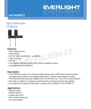
The ITR8104 is a compact opto interrupter module designed for non-contact sensing and switching applications. It integrates an infrared emitting diode and an NPN silicon phototransistor within a single, black thermoplastic housing. The components are arranged side-by-side on converging optical axes. In its normal state, the phototransistor receives infrared radiation emitted by the LED. When an opaque object interrupts the light path between the emitter and detector, the phototransistor ceases to conduct, providing a clear switching signal.
Key advantages of this device include a fast response time, high sensitivity, and a peak emission wavelength of 940nm, which is outside the visible spectrum to minimize interference from ambient light. The device is constructed with lead-free materials and complies with relevant environmental regulations such as RoHS and EU REACH.
2. Technical Specifications Deep Dive
2.1 Absolute Maximum Ratings
Operating the device beyond these limits may cause permanent damage.
- Input (IR LED):
- Power Dissipation (Pd): 75 mW (at or below 25°C)
- Reverse Voltage (VR): 5 V
- Forward Current (IF): 50 mA
- Output (Phototransistor):
- Collector Power Dissipation (Pc): 75 mW
- Collector Current (IC): 20 mA
- Collector-Emitter Voltage (BVCEO): 30 V
- Emitter-Collector Voltage (BVECO): 5 V
- Thermal:
- Operating Temperature (Topr): -25°C to +85°C
- Storage Temperature (Tstg): -40°C to +85°C
- Lead Soldering Temperature (Tsol): 260°C for ≤5 seconds (measured 3mm from package)
2.2 Electro-Optical Characteristics (Ta=25°C)
These parameters define the device's performance under typical operating conditions.
- Input (IR LED) Characteristics:
- Forward Voltage (VF): 1.2V (Typical), 1.6V (Maximum) at IF=20mA
- Reverse Current (IR): 10 μA (Maximum) at VR=5V
- Peak Wavelength (λP): 940 nm (Typical) at IF=20mA
- Output (Phototransistor) Characteristics:
- Dark Current (ICEO): 100 nA (Maximum) at VCE=20V, Ee=0mW/cm²
- Collector-Emitter Saturation Voltage (VCE(sat)): 0.4V (Maximum) at IC=0.5mA, IF=20mA
- Collector Current (IC(ON)): 0.5 mA (Minimum) at VCE=5V, IF=20mA
- Rise Time (tr): 20 μs (Typical) at VCE=5V, IC=1mA, RL=1kΩ
- Fall Time (tf): 20 μs (Typical) at VCE=5V, IC=1mA, RL=1kΩ
3. Performance Curve Analysis
The datasheet provides several characteristic curves essential for design engineers.
3.1 IR LED Characteristics
Graphs illustrate the relationship between forward current and ambient temperature, showing necessary derating at higher temperatures to stay within power limits. The spectral sensitivity curve confirms the peak emission at 940nm. Another graph shows the minor variation of peak emission wavelength with ambient temperature, which is typically negligible for most applications.
3.2 Phototransistor Characteristics
Key graphs include the relationship between collector current and forward current (transfer characteristics) at various temperatures, highlighting the device's sensitivity. The collector power dissipation vs. ambient temperature graph is crucial for thermal management, indicating how maximum allowable power decreases as ambient temperature rises.
4. Mechanical and Package Information
4.1 Package Dimensions
The ITR8104 comes in a standard through-hole package. Critical dimensions include the lead spacing, body width, and overall height. All dimensions are in millimeters with a general tolerance of ±0.3mm unless otherwise specified. The lead spacing is measured at the point where the leads emerge from the plastic package body.
4.2 Polarity Identification and Mounting
The device has a standard pinout: the infrared LED anode and cathode, and the phototransistor collector and emitter. The housing is typically marked or shaped to indicate pin 1. When mounting on a PCB, holes must be precisely aligned with the lead positions to avoid imposing mechanical stress on the epoxy body, which can degrade performance or cause failure.
5. Soldering and Assembly Guidelines
5.1 Lead Forming
- Bending must be performed at a distance greater than 3mm from the bottom of the epoxy resin body.
- Lead forming must be completed before the soldering process.
- The lead frame must be securely held during bending to prevent stress on the package.
- Cutting of leads should be done at room temperature.
5.2 Soldering Recommendations
To prevent thermal damage, maintain a minimum distance of 3mm from the solder joint to the epoxy bulb.
- Hand Soldering: Iron tip temperature: 300°C Max. (30W Max.). Soldering time: 3 seconds Max. per lead.
- Wave/Dip Soldering: Preheat temperature: 100°C Max. (60 sec Max.). Solder bath temperature: 260°C Max. Dwell time: 5 seconds Max.
- Avoid rapid cooling after soldering. Allow the device to return to room temperature gradually.
- Dip or hand soldering should not be performed more than once.
5.3 Recommended Soldering Profile
The profile suggests a gradual preheat, a controlled time above liquidus (typically 260°C), and a controlled cooling rate to minimize thermal shock to the component.
6. Storage and Handling
- Initial Storage (after shipping): 10–30°C, ≤70% RH for up to 3 months.
- Long-term Storage (beyond 3 months): 10–25°C, 20–60% RH in a sealed container with a nitrogen atmosphere for up to one year.
- After Opening Package: Store at 10–25°C, 20–60% RH. Use within 24 hours or as soon as possible. Reseal unused devices promptly.
- Avoid rapid temperature changes in high-humidity environments to prevent condensation.
- Cleaning: Ultrasonic cleaning is not recommended for this device.
7. Packaging and Ordering Information
7.1 Packing Specification
The standard packaging is: 100 pieces per tube, 20 tubes per box, and 4 boxes per carton.
7.2 Label Information
The product label includes fields for: Customer's Product Number (CPN), Product Number (P/N), Packing Quantity (QTY), Luminous Intensity Rank (CAT), Dominant Wavelength Rank (HUE), Forward Voltage Rank (REF), Lot Number (LOT No.), and a date/month code (X).
8. Application Suggestions
8.1 Typical Application Scenarios
- Position/Speed Sensing: In computer mice, copiers, and floppy disk drives to detect rotation or linear movement.
- Non-contact Switching: Object detection in vending machines, security systems, and industrial automation.
- Edge Detection: In printers and scanners to detect paper presence or media edges.
- Direct Board Mounting: Suitable for through-hole PCB applications where reliable, isolated switching is required.
8.2 Design Considerations
- Current Limiting: Always use a series resistor with the IR LED to limit forward current (IF) to the desired value, typically 20mA or less for long-term reliability.
- Load Resistor: A pull-up resistor is typically connected between the phototransistor's collector and the supply voltage (VCC). The value (e.g., 1kΩ) affects output voltage swing and switching speed.
- Ambient Light: While the 940nm filter helps, designing a physical barrier or housing to shield the sensor from direct ambient IR sources (like sunlight or incandescent bulbs) improves reliability.
- Response Time: For high-speed applications, consider the 20μs typical rise/fall time and ensure the driving circuit can accommodate it.
- Thermal Management: Adhere to the power derating curves, especially in high ambient temperature environments.
9. Technical Comparison and Differentiation
The ITR8104 offers a balanced set of characteristics. Its 940nm wavelength provides good immunity to visible light noise. The side-by-side, converging axis design offers a well-defined sensing gap, making it suitable for edge detection and precise object positioning. The fast 20μs response time enables use in moderate-speed counting or encoding applications. The through-hole package provides robust mechanical attachment for applications subject to vibration. When compared to reflective sensors, interrupters provide a more definitive on/off signal as they are not affected by the reflectivity of the target object.
10. Frequently Asked Questions (Based on Technical Parameters)
10.1 What is the typical operating current for the IR LED?
The electro-optical characteristics are specified at IF = 20mA, which is a common and reliable operating point. It can be driven up to the absolute maximum of 50mA for higher output, but this requires careful thermal management and may reduce long-term reliability.
10.2 How sensitive is the phototransistor?
The key parameter is IC(ON), which is guaranteed to be at least 0.5mA when the IR LED is driven with 20mA and VCE=5V. This provides a solid signal for digital switching interfaces with a suitable pull-up resistor.
10.3 Can I use this for sensing transparent objects?
No. The ITR8104 is designed for detecting opaque objects that completely interrupt the infrared beam. Transparent or translucent materials may allow enough IR light to pass through, preventing the phototransistor from turning fully off.
10.4 What is the recommended gap between the emitter and detector for an object?
The datasheet does not specify a maximum gap. The effective gap is determined by the alignment and the intensity of the IR LED. For reliable operation, the object should fully occupy the converging optical path between the two elements. The typical sensing distance is a few millimeters, defined by the mechanical housing.
11. Practical Design and Usage Case
Case: Paper Jam Detection in a Printer
An ITR8104 is mounted across the paper path. A microcontroller pin drives the IR LED through a 150Ω resistor (limiting IF to ~20mA at 3.3V). The phototransistor collector is connected to the microcontroller's digital input pin via a 4.7kΩ pull-up resistor to 3.3V. In the "paper present" state, the paper blocks the beam, the phototransistor is off, and the input pin reads HIGH via the pull-up. When the paper path is clear, the IR light reaches the phototransistor, turning it on and pulling the input pin LOW. The microcontroller monitors this pin. A persistent HIGH state when paper is expected indicates a jam or misfeed. The fast response time ensures the jam is detected quickly, and the 940nm wavelength prevents false triggers from room lighting.
12. Operating Principle
The ITR8104 operates on the principle of modulated light detection. An infrared LED emits photons at a wavelength of 940nm. A silicon phototransistor, positioned opposite the LED, acts as the receiver. When photons of sufficient energy strike the base region of the phototransistor, they generate electron-hole pairs. This photogenerated current acts as base current, causing the transistor to conduct a much larger collector current (the photoelectric effect combined with transistor amplification). The presence of an opaque object in the light path stops photons from reaching the phototransistor, eliminating the base current and turning the transistor off. This creates a digital output signal correlated to the presence or absence of the object.
13. Technology Trends
Opto interrupters remain fundamental components in electromechanical systems. Current trends focus on miniaturization (smaller SMD packages), integration of additional signal conditioning circuitry (like Schmitt triggers or amplifiers) within the package to provide a cleaner digital output, and improved resistance to environmental contaminants. There is also a trend towards higher speed variants for advanced encoding applications. The core principle of optical interruption remains robust due to its electrical isolation, non-contact nature, and reliability compared to purely mechanical switches.
LED Specification Terminology
Complete explanation of LED technical terms
Photoelectric Performance
| Term | Unit/Representation | Simple Explanation | Why Important |
|---|---|---|---|
| Luminous Efficacy | lm/W (lumens per watt) | Light output per watt of electricity, higher means more energy efficient. | Directly determines energy efficiency grade and electricity cost. |
| Luminous Flux | lm (lumens) | Total light emitted by source, commonly called "brightness". | Determines if the light is bright enough. |
| Viewing Angle | ° (degrees), e.g., 120° | Angle where light intensity drops to half, determines beam width. | Affects illumination range and uniformity. |
| CCT (Color Temperature) | K (Kelvin), e.g., 2700K/6500K | Warmth/coolness of light, lower values yellowish/warm, higher whitish/cool. | Determines lighting atmosphere and suitable scenarios. |
| CRI / Ra | Unitless, 0–100 | Ability to render object colors accurately, Ra≥80 is good. | Affects color authenticity, used in high-demand places like malls, museums. |
| SDCM | MacAdam ellipse steps, e.g., "5-step" | Color consistency metric, smaller steps mean more consistent color. | Ensures uniform color across same batch of LEDs. |
| Dominant Wavelength | nm (nanometers), e.g., 620nm (red) | Wavelength corresponding to color of colored LEDs. | Determines hue of red, yellow, green monochrome LEDs. |
| Spectral Distribution | Wavelength vs intensity curve | Shows intensity distribution across wavelengths. | Affects color rendering and quality. |
Electrical Parameters
| Term | Symbol | Simple Explanation | Design Considerations |
|---|---|---|---|
| Forward Voltage | Vf | Minimum voltage to turn on LED, like "starting threshold". | Driver voltage must be ≥Vf, voltages add up for series LEDs. |
| Forward Current | If | Current value for normal LED operation. | Usually constant current drive, current determines brightness & lifespan. |
| Max Pulse Current | Ifp | Peak current tolerable for short periods, used for dimming or flashing. | Pulse width & duty cycle must be strictly controlled to avoid damage. |
| Reverse Voltage | Vr | Max reverse voltage LED can withstand, beyond may cause breakdown. | Circuit must prevent reverse connection or voltage spikes. |
| Thermal Resistance | Rth (°C/W) | Resistance to heat transfer from chip to solder, lower is better. | High thermal resistance requires stronger heat dissipation. |
| ESD Immunity | V (HBM), e.g., 1000V | Ability to withstand electrostatic discharge, higher means less vulnerable. | Anti-static measures needed in production, especially for sensitive LEDs. |
Thermal Management & Reliability
| Term | Key Metric | Simple Explanation | Impact |
|---|---|---|---|
| Junction Temperature | Tj (°C) | Actual operating temperature inside LED chip. | Every 10°C reduction may double lifespan; too high causes light decay, color shift. |
| Lumen Depreciation | L70 / L80 (hours) | Time for brightness to drop to 70% or 80% of initial. | Directly defines LED "service life". |
| Lumen Maintenance | % (e.g., 70%) | Percentage of brightness retained after time. | Indicates brightness retention over long-term use. |
| Color Shift | Δu′v′ or MacAdam ellipse | Degree of color change during use. | Affects color consistency in lighting scenes. |
| Thermal Aging | Material degradation | Deterioration due to long-term high temperature. | May cause brightness drop, color change, or open-circuit failure. |
Packaging & Materials
| Term | Common Types | Simple Explanation | Features & Applications |
|---|---|---|---|
| Package Type | EMC, PPA, Ceramic | Housing material protecting chip, providing optical/thermal interface. | EMC: good heat resistance, low cost; Ceramic: better heat dissipation, longer life. |
| Chip Structure | Front, Flip Chip | Chip electrode arrangement. | Flip chip: better heat dissipation, higher efficacy, for high-power. |
| Phosphor Coating | YAG, Silicate, Nitride | Covers blue chip, converts some to yellow/red, mixes to white. | Different phosphors affect efficacy, CCT, and CRI. |
| Lens/Optics | Flat, Microlens, TIR | Optical structure on surface controlling light distribution. | Determines viewing angle and light distribution curve. |
Quality Control & Binning
| Term | Binning Content | Simple Explanation | Purpose |
|---|---|---|---|
| Luminous Flux Bin | Code e.g., 2G, 2H | Grouped by brightness, each group has min/max lumen values. | Ensures uniform brightness in same batch. |
| Voltage Bin | Code e.g., 6W, 6X | Grouped by forward voltage range. | Facilitates driver matching, improves system efficiency. |
| Color Bin | 5-step MacAdam ellipse | Grouped by color coordinates, ensuring tight range. | Guarantees color consistency, avoids uneven color within fixture. |
| CCT Bin | 2700K, 3000K etc. | Grouped by CCT, each has corresponding coordinate range. | Meets different scene CCT requirements. |
Testing & Certification
| Term | Standard/Test | Simple Explanation | Significance |
|---|---|---|---|
| LM-80 | Lumen maintenance test | Long-term lighting at constant temperature, recording brightness decay. | Used to estimate LED life (with TM-21). |
| TM-21 | Life estimation standard | Estimates life under actual conditions based on LM-80 data. | Provides scientific life prediction. |
| IESNA | Illuminating Engineering Society | Covers optical, electrical, thermal test methods. | Industry-recognized test basis. |
| RoHS / REACH | Environmental certification | Ensures no harmful substances (lead, mercury). | Market access requirement internationally. |
| ENERGY STAR / DLC | Energy efficiency certification | Energy efficiency and performance certification for lighting. | Used in government procurement, subsidy programs, enhances competitiveness. |