Table of Contents
- 1. Product Overview
- 2. Key Features and Compliance
- 3. Device Selection and Construction
- 4. Absolute Maximum Ratings
- 4.1 Input (Infrared Emitter) Ratings
- 4.2 Output (Phototransistor) Ratings
- 4.3 General Ratings
- 5. Electro-Optical Characteristics
- 5.1 Infrared Emitter (Input) Characteristics
- 5.2 Phototransistor (Output) Characteristics
- 6. Performance Curve Analysis
- 6.1 Infrared Emitter Curves
- 6.2 Phototransistor Curves
- 7. Mechanical and Package Information
- 7.1 Package Dimensions
- 7.2 Polarity Identification
- 8. Soldering and Assembly Guidelines
- 9. Packaging and Ordering Information
- 10. Application Suggestions
- 10.1 Typical Application Scenarios
- 10.2 Design Considerations
- 11. Technical Comparison and Advantages
- 12. Frequently Asked Questions (Based on Technical Parameters)
- 13. Operational Principle
- 14. Disclaimer and Usage Notes
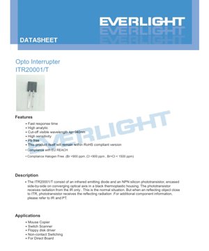
1. Product Overview
The ITR20001/T is a reflective opto interrupter module designed for non-contact sensing applications. It integrates an infrared emitting diode and an NPN silicon phototransistor within a single, compact black thermoplastic housing. The components are positioned side-by-side on converging optical axes. In its default state, the phototransistor does not receive radiation from the emitter. When a reflective object enters the sensing gap, infrared light from the emitter reflects off the object and is detected by the phototransistor, causing a change in its output state. This principle enables reliable object detection and position sensing.
2. Key Features and Compliance
The device offers several advantages for electronic design:
- Fast Response Time: Enables quick detection suitable for high-speed applications.
- High Sensitivity: The phototransistor provides a strong output signal relative to the input irradiance.
- Infrared Operation: Features a peak emission wavelength (λp) of 940nm, which is invisible to the human eye, reducing ambient light interference.
- Environmental Compliance: The product is Pb-free, compliant with RoHS and EU REACH regulations, and is Halogen Free (Br <900 ppm, Cl <900 ppm, Br+Cl < 1500 ppm).
3. Device Selection and Construction
The module is constructed with specific materials for optimal performance:
- Infrared Emitter (IR): Utilizes a GaAlAs (Gallium Aluminum Arsenide) chip, housed behind a water-clear lens for efficient infrared transmission.
- Phototransistor (PT): Utilizes a Silicon chip, housed behind a black lens to filter out visible light and improve signal-to-noise ratio.
The black housing minimizes internal light reflections (crosstalk) between the emitter and detector when no object is present, ensuring a reliable off-state.
4. Absolute Maximum Ratings
Operating the device beyond these limits may cause permanent damage. All ratings are specified at an ambient temperature (Ta) of 25°C.
4.1 Input (Infrared Emitter) Ratings
- Power Dissipation (Pd): 75 mW
- Reverse Voltage (VR): 5 V
- Continuous Forward Current (IF): 50 mA
- Peak Forward Current (IFP): 1 A (Pulse width ≤100μs, Duty cycle=1%)
4.2 Output (Phototransistor) Ratings
- Collector Power Dissipation (Pd): 75 mW
- Collector Current (IC): 20 mA
- Collector-Emitter Voltage (BVCEO): 30 V
- Emitter-Collector Voltage (BVECO): 5 V
4.3 General Ratings
- Operating Temperature (Topr): -40°C to +85°C
- Storage Temperature (Tstg): -40°C to +85°C
- Lead Soldering Temperature (Tsol): 260°C for 5 seconds (measured 1/16 inch from the package body).
5. Electro-Optical Characteristics
These parameters define the electrical and optical performance under standard test conditions (Ta=25°C).
5.1 Infrared Emitter (Input) Characteristics
- Forward Voltage (VF): 1.2 V (Typical) at IF = 20mA. Maximum is 1.5V.
- Reverse Current (IR): Maximum 10 μA at VR = 5V.
- Peak Wavelength (λP): 940 nm (Typical) at IF = 20mA.
5.2 Phototransistor (Output) Characteristics
- Dark Current (ICEO): Maximum 100 nA at VCE = 5V with zero irradiance (Ee=0). This is the leakage current when the sensor is off.
- Collector-Emitter Saturation Voltage (VCE(sat)): Maximum 0.4 V at IC = 2mA and an irradiance of 1 mW/cm². A low VCE(sat) is desirable for switching applications.
- Collector Current (Transfer Ratio):
- IC(ON): Minimum 200 μA at VCE = 5V and IF = 20mA. This is the current when an object is detected.
- IC(OFF): Maximum 2 μA under the same conditions, representing the residual current when no object is present.
- Switching Speed:
- Rise Time (tr): 25 μs (Typical)
- Fall Time (tf): 25 μs (Typical) Measured with VCE=5V, IC=100μA, and RL=100Ω.
6. Performance Curve Analysis
The datasheet provides graphical data illustrating device behavior under various conditions.
6.1 Infrared Emitter Curves
- Forward Current vs. Ambient Temperature: Shows the derating of maximum allowable forward current as temperature increases.
- Spectral Sensitivity: Confirms the narrow emission band centered around 940nm.
- Peak Emission Wavelength vs. Temperature: Illustrates the slight shift in peak wavelength with changing temperature.
- Forward Current vs. Forward Voltage (IV Curve): Provides the relationship for calculating series resistor values.
- Radiant Intensity vs. Forward Current: Shows the optical output power as a function of drive current.
- Relative Radiant Intensity vs. Angular Displacement: Depicts the emission pattern (beam profile) of the IR LED.
6.2 Phototransistor Curves
- Collector Power Dissipation vs. Ambient Temperature: Provides derating guidelines for the phototransistor's power handling.
- Spectral Sensitivity: Shows the phototransistor's responsivity across wavelengths, peaking in the infrared region to match the emitter.
- Relative Collector Current vs. Ambient Temperature: Indicates how the phototransistor's sensitivity changes with temperature.
- Collector Current vs. Irradiance: A key graph showing the linear relationship between incident light power and output current, defining the device's transfer characteristic.
- Collector Dark Current vs. Ambient Temperature: Shows how leakage current increases with temperature, important for high-temperature operation.
- Collector Current vs. Collector-Emitter Voltage: Output characteristic curves showing the phototransistor operating in its active and saturation regions under different irradiance levels.
7. Mechanical and Package Information
The ITR20001/T is housed in a compact, surface-mount compatible package.
7.1 Package Dimensions
The key dimensions from the provided drawing are approximately 4.0mm in length, 4.0mm in width, and 2.5mm in height (excluding leads). The lead spacing is designed for standard PCB mounting. A critical note specifies a minimum 10.0mm aluminum evaporation area, likely referring to a recommended keep-out zone or heat dissipation feature on the PCB. All unspecified tolerances are ±0.25mm.
7.2 Polarity Identification
The package includes markings or a specific shape to identify the anode and cathode of the IR emitter and the collector and emitter of the phototransistor. Designers must consult the dimensional drawing for precise pinout information to ensure correct PCB layout and assembly.
8. Soldering and Assembly Guidelines
The device is rated for lead soldering at 260°C for 5 seconds, measured 1/16 inch (approximately 1.6mm) from the package body. This is compatible with standard infrared (IR) or convection reflow soldering processes using lead-free (Sn-Ag-Cu) solder paste. Care should be taken to follow the recommended reflow profile to avoid thermal shock or damage to the plastic housing. The device should be stored in a dry, controlled environment prior to use.
9. Packaging and Ordering Information
The standard packing specification is as follows:
- 200 pieces per bag.
- 6 bags per box.
- 10 boxes per carton.
The product label includes fields for Customer Part Number (CPN), Manufacturer Part Number (P/N), Quantity (QTY), and various ranking codes for luminous intensity (CAT), dominant wavelength (HUE), and forward voltage (REF). A Lot Number and date code (identified by 'X' for month) are also provided for traceability.
10. Application Suggestions
10.1 Typical Application Scenarios
The ITR20001/T is well-suited for a variety of non-contact sensing and switching applications, including:
- Mouse and Copier Mechanisms: Detecting wheel or encoder disk rotation.
- Switch and Scanner Systems: Object presence detection for automatic doors, vending machines, or paper detection in printers.
- Floppy Disk Drives: Historically used for detecting the write-protect tab or disk insertion.
- General Non-contact Switching: Any application requiring object detection, counting, or limit sensing without physical contact.
- Direct Board Mounting: Its compact SMD package makes it ideal for space-constrained PCB designs.
10.2 Design Considerations
- Current Limiting Resistor: A series resistor must be used with the IR emitter to limit the forward current (IF) to a safe value, typically 20mA for normal operation. Calculate using R = (VCC - VF) / IF.
- Load Resistor: A pull-up resistor is typically connected between the phototransistor's collector and the supply voltage (VCC). The value of this resistor (RL) determines the output voltage swing and switching speed. A smaller RL provides faster switching but lower output voltage variation.
- Ambient Light: While the black lens and 940nm filtering reduce interference, very strong ambient infrared sources (e.g., sunlight, incandescent bulbs) may affect performance. Shielding or optical filtering may be necessary in harsh environments.
- Reflective Surface: The sensing distance and reliability depend on the reflectivity of the target object. White or metallic surfaces provide the best response; dark or matte surfaces may require reduced gap distances.
- Alignment: The converging optical axes define a specific sensing gap. The object must pass within this gap for reliable detection.
11. Technical Comparison and Advantages
Compared to mechanical switches or other optical sensors, the ITR20001/T offers distinct benefits:
- vs. Mechanical Switches: Provides non-contact operation, eliminating wear and tear, enabling higher switching speeds, and offering silent operation. It is immune to contact bounce.
- vs. Photodiode-Based Sensors: The integrated phototransistor provides current gain, resulting in higher output current for a given light input, often eliminating the need for an additional amplifier stage in simple on/off detection circuits.
- vs. Discrete Emitter-Detector Pairs: The pre-aligned, housed module simplifies design and assembly, ensures consistent optical alignment, and saves board space. The integrated black housing minimizes internal crosstalk.
12. Frequently Asked Questions (Based on Technical Parameters)
Q: What is the typical sensing distance?
A: The sensing distance is not a fixed parameter; it depends on the drive current to the IR emitter, the reflectivity of the target object, and the required output current from the phototransistor. Designers should use the "Collector Current vs. Irradiance" graph and the "Radiant Intensity vs. Forward Current" graph to calculate the expected signal for a specific gap and reflectivity.
Q: Can I drive the IR emitter with a voltage source directly?
A: No. The IR emitter is a diode and must have its current limited by an external series resistor to prevent damage from overcurrent, as specified by the Absolute Maximum Ratings (IF max = 50mA).
Q: How do I interface the output to a microcontroller?
A: The simplest method is to use the phototransistor as a switch. Connect a pull-up resistor (e.g., 10kΩ) from the collector to the microcontroller's logic voltage (e.g., 3.3V or 5V). Connect the emitter to ground. The collector node will be pulled high (logic 1) when no object is detected (dark) and will be pulled low (logic 0) when an object reflects light onto the phototransistor, turning it on.
Q: Why is the response time specified with a 100Ω load resistor?
A> Switching speed is affected by the RC time constant formed by the phototransistor's junction capacitance and the load resistance (RL). A smaller RL (like 100Ω) gives a faster time constant, allowing measurement of the intrinsic speed of the device. In a real application with a larger RL for higher voltage swing, the switching speed will be slower.
13. Operational Principle
The ITR20001/T operates on the principle of modulated light reflection. The internal infrared LED emits light at 940nm. The phototransistor, which is sensitive to this wavelength, is positioned such that it does not directly "see" the LED's light beam under normal conditions (no object present). Its output remains in a high-impedance/low-current state (dark current). When a reflective object enters the predefined gap between the emitter and detector, it reflects a portion of the infrared light onto the phototransistor's active area. This incident light generates base current in the phototransistor, causing it to turn on and conduct a significantly higher collector current (IC(ON)). This change in current/voltage at the output pins is detected by the external circuit, signaling the presence of the object.
14. Disclaimer and Usage Notes
Critical disclaimers from the datasheet must be observed:
- The manufacturer reserves the right to adjust product materials.
- The product meets published specifications for 12 months from the shipment date.
- Graphs and typical values are for reference only and are not guaranteed.
- The Absolute Maximum Ratings must not be exceeded. The manufacturer assumes no responsibility for damage resulting from misuse.
- The product is not intended for use in safety-critical, military, aviation, automotive, medical, or life-sustaining applications without prior consultation and approval.
LED Specification Terminology
Complete explanation of LED technical terms
Photoelectric Performance
| Term | Unit/Representation | Simple Explanation | Why Important |
|---|---|---|---|
| Luminous Efficacy | lm/W (lumens per watt) | Light output per watt of electricity, higher means more energy efficient. | Directly determines energy efficiency grade and electricity cost. |
| Luminous Flux | lm (lumens) | Total light emitted by source, commonly called "brightness". | Determines if the light is bright enough. |
| Viewing Angle | ° (degrees), e.g., 120° | Angle where light intensity drops to half, determines beam width. | Affects illumination range and uniformity. |
| CCT (Color Temperature) | K (Kelvin), e.g., 2700K/6500K | Warmth/coolness of light, lower values yellowish/warm, higher whitish/cool. | Determines lighting atmosphere and suitable scenarios. |
| CRI / Ra | Unitless, 0–100 | Ability to render object colors accurately, Ra≥80 is good. | Affects color authenticity, used in high-demand places like malls, museums. |
| SDCM | MacAdam ellipse steps, e.g., "5-step" | Color consistency metric, smaller steps mean more consistent color. | Ensures uniform color across same batch of LEDs. |
| Dominant Wavelength | nm (nanometers), e.g., 620nm (red) | Wavelength corresponding to color of colored LEDs. | Determines hue of red, yellow, green monochrome LEDs. |
| Spectral Distribution | Wavelength vs intensity curve | Shows intensity distribution across wavelengths. | Affects color rendering and quality. |
Electrical Parameters
| Term | Symbol | Simple Explanation | Design Considerations |
|---|---|---|---|
| Forward Voltage | Vf | Minimum voltage to turn on LED, like "starting threshold". | Driver voltage must be ≥Vf, voltages add up for series LEDs. |
| Forward Current | If | Current value for normal LED operation. | Usually constant current drive, current determines brightness & lifespan. |
| Max Pulse Current | Ifp | Peak current tolerable for short periods, used for dimming or flashing. | Pulse width & duty cycle must be strictly controlled to avoid damage. |
| Reverse Voltage | Vr | Max reverse voltage LED can withstand, beyond may cause breakdown. | Circuit must prevent reverse connection or voltage spikes. |
| Thermal Resistance | Rth (°C/W) | Resistance to heat transfer from chip to solder, lower is better. | High thermal resistance requires stronger heat dissipation. |
| ESD Immunity | V (HBM), e.g., 1000V | Ability to withstand electrostatic discharge, higher means less vulnerable. | Anti-static measures needed in production, especially for sensitive LEDs. |
Thermal Management & Reliability
| Term | Key Metric | Simple Explanation | Impact |
|---|---|---|---|
| Junction Temperature | Tj (°C) | Actual operating temperature inside LED chip. | Every 10°C reduction may double lifespan; too high causes light decay, color shift. |
| Lumen Depreciation | L70 / L80 (hours) | Time for brightness to drop to 70% or 80% of initial. | Directly defines LED "service life". |
| Lumen Maintenance | % (e.g., 70%) | Percentage of brightness retained after time. | Indicates brightness retention over long-term use. |
| Color Shift | Δu′v′ or MacAdam ellipse | Degree of color change during use. | Affects color consistency in lighting scenes. |
| Thermal Aging | Material degradation | Deterioration due to long-term high temperature. | May cause brightness drop, color change, or open-circuit failure. |
Packaging & Materials
| Term | Common Types | Simple Explanation | Features & Applications |
|---|---|---|---|
| Package Type | EMC, PPA, Ceramic | Housing material protecting chip, providing optical/thermal interface. | EMC: good heat resistance, low cost; Ceramic: better heat dissipation, longer life. |
| Chip Structure | Front, Flip Chip | Chip electrode arrangement. | Flip chip: better heat dissipation, higher efficacy, for high-power. |
| Phosphor Coating | YAG, Silicate, Nitride | Covers blue chip, converts some to yellow/red, mixes to white. | Different phosphors affect efficacy, CCT, and CRI. |
| Lens/Optics | Flat, Microlens, TIR | Optical structure on surface controlling light distribution. | Determines viewing angle and light distribution curve. |
Quality Control & Binning
| Term | Binning Content | Simple Explanation | Purpose |
|---|---|---|---|
| Luminous Flux Bin | Code e.g., 2G, 2H | Grouped by brightness, each group has min/max lumen values. | Ensures uniform brightness in same batch. |
| Voltage Bin | Code e.g., 6W, 6X | Grouped by forward voltage range. | Facilitates driver matching, improves system efficiency. |
| Color Bin | 5-step MacAdam ellipse | Grouped by color coordinates, ensuring tight range. | Guarantees color consistency, avoids uneven color within fixture. |
| CCT Bin | 2700K, 3000K etc. | Grouped by CCT, each has corresponding coordinate range. | Meets different scene CCT requirements. |
Testing & Certification
| Term | Standard/Test | Simple Explanation | Significance |
|---|---|---|---|
| LM-80 | Lumen maintenance test | Long-term lighting at constant temperature, recording brightness decay. | Used to estimate LED life (with TM-21). |
| TM-21 | Life estimation standard | Estimates life under actual conditions based on LM-80 data. | Provides scientific life prediction. |
| IESNA | Illuminating Engineering Society | Covers optical, electrical, thermal test methods. | Industry-recognized test basis. |
| RoHS / REACH | Environmental certification | Ensures no harmful substances (lead, mercury). | Market access requirement internationally. |
| ENERGY STAR / DLC | Energy efficiency certification | Energy efficiency and performance certification for lighting. | Used in government procurement, subsidy programs, enhances competitiveness. |