Table of Contents
- 1. Product Overview
- 1.1 Core Features and Advantages
- 1.2 Target Applications
- 2. In-Depth Technical Parameter Analysis
- 2.1 Absolute Maximum Ratings
- 2.2 Electro-Optical Characteristics
- 3. Performance Curve Analysis
- 3.1 IR Emitter Characteristics
- 3.2 Phototransistor Characteristics
- 4. Mechanical and Package Information
- 4.1 Package Dimensions
- 4.2 Polarity Identification and Mounting
- 5. Soldering and Assembly Guidelines
- 5.1 Lead Forming Instructions
- 5.2 Recommended Soldering Parameters
- 5.3 Storage Conditions
- 6. Packaging and Ordering Information
- 6.1 Packing Specifications
- 6.2 Label Information
- 7. Application Design Considerations
- 7.1 Typical Circuit Configuration
- 7.2 Design and Layout Best Practices
- 8. Technical Comparison and Differentiation
- 9. Frequently Asked Questions (FAQ)
- 9.1 Based on Technical Parameters
- 10. Practical Application Examples
- 10.1 Paper Detection in a Printer
- 10.2 Rotary Encoder for Motor Speed
- 11. Operating Principle
- 12. Technology Trends
1. Product Overview
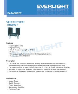
The ITR9606-F is a compact, side-by-side reflective opto interrupter module. It integrates an infrared emitting diode (IRED) and a silicon phototransistor within a single black thermoplastic housing. The components are aligned on converging optical axes. The fundamental operating principle involves the phototransistor detecting radiation emitted by the IRED. When an opaque object interrupts the light path between the emitter and detector, the phototransistor's output state changes, enabling non-contact sensing and switching functions.
1.1 Core Features and Advantages
- Fast Response Time: Enables high-speed detection suitable for applications like encoders and speed sensors.
- High Sensitivity: The silicon phototransistor provides reliable signal detection even with low IR intensity.
- Specific Wavelength: Features a peak emission wavelength (λp) of 940nm, which is in the near-infrared spectrum, minimizing interference from ambient visible light.
- Environmental Compliance: The product is Pb-free, compliant with the RoHS directive, and adheres to EU REACH regulations.
- Compact Design: The integrated side-by-side package offers a space-saving solution for PCB mounting.
1.2 Target Applications
This opto interrupter is designed for a variety of non-contact sensing and position detection applications, including but not limited to:
- Position sensing in computer mice and copiers.
- Paper detection and edge sensing in scanners and printers.
- Disk presence detection in floppy disk drives and other media drives.
- General-purpose non-contact switching.
- Direct board mounting in consumer electronics and industrial controls.
2. In-Depth Technical Parameter Analysis
This section provides a detailed, objective interpretation of the device's electrical and optical specifications.
2.1 Absolute Maximum Ratings
These ratings define the limits beyond which permanent damage to the device may occur. Operation under these conditions is not guaranteed.
- Input (IRED):
- Power Dissipation (Pd): 75 mW (at or below 25°C). Requires derating at higher ambient temperatures.
- Reverse Voltage (VR): 5 V. Exceeding this can damage the LED junction.
- Forward Current (IF): 50 mA. The continuous DC current should typically be limited to 20mA for reliable long-term operation.
- Output (Phototransistor):
- Collector Power Dissipation (Pd): 75 mW.
- Collector Current (IC): 20 mA.
- Collector-Emitter Voltage (BVCEO): 30 V.
- Emitter-Collector Voltage (BVECO): 5 V.
- Thermal Limits:
- Operating Temperature (Topr): -25°C to +85°C.
- Storage Temperature (Tstg): -40°C to +85°C.
- Lead Soldering Temperature (Tsol): 260°C for a maximum of 5 seconds, measured 3mm from the package body.
2.2 Electro-Optical Characteristics
Measured at Ta = 25°C, these parameters define the device's typical performance under normal operating conditions.
- Input (IRED) Characteristics:
- Forward Voltage (VF): Typically 1.2V, with a maximum of 1.5V at IF=20mA. This is crucial for designing the current-limiting circuit for the LED.
- Reverse Current (IR): Maximum 10 μA at VR=5V.
- Peak Wavelength (λP): 940 nm. This IR wavelength is invisible to the human eye and helps reduce optical noise.
- Output (Phototransistor) Characteristics:
- Dark Current (ICEO): Maximum 100 nA at VCE=20V with zero illumination (Ee=0). This is the leakage current when the sensor is blocked.
- Collector-Emitter Saturation Voltage (VCE(sat)): Maximum 0.4V at IC=2mA and an irradiance of 1mW/cm². A lower VCE(sat) is better for digital switching applications.
- Collector Current (IC(ON)): Ranges from a minimum of 0.5mA to a maximum of 10mA at VCE=5V and IF=20mA. This wide range indicates potential unit-to-unit variation in sensitivity.
- Dynamic Response:
- Rise Time (tr) & Fall Time (tf): Typically 15 μs each under specified test conditions (VCE=5V, IC=1mA, RL=1kΩ). This defines the maximum switching frequency capability.
3. Performance Curve Analysis
Graphical data provides deeper insight into device behavior under varying conditions.
3.1 IR Emitter Characteristics
The datasheet includes typical curves for the infrared emitter component.
- Forward Current vs. Forward Voltage (IF-VF Curve): This exponential curve is standard for a diode. At the typical operating point of IF=20mA, VF is approximately 1.2V. The curve helps in thermal management analysis, as VF has a negative temperature coefficient.
- Spectral Distribution: Confirms the peak emission at 940nm with a typical full width at half maximum (FWHM) for a GaAlAs LED, showing minimal emission in the visible spectrum.
3.2 Phototransistor Characteristics
- Spectral Sensitivity: The silicon phototransistor has peak sensitivity in the near-infrared region, closely matching the 940nm emission of the paired IRED. This alignment maximizes coupling efficiency and signal-to-noise ratio.
- Collector Power Dissipation vs. Ambient Temperature: A derating curve that shows the maximum allowable power dissipation decreases linearly as ambient temperature increases above 25°C. This is critical for reliability calculations in high-temperature environments.
4. Mechanical and Package Information
4.1 Package Dimensions
The ITR9606-F has a compact, rectangular housing.
- Overall Dimensions: Approximately 4.0mm in length, 3.2mm in width, and 2.5mm in height (excluding leads).
- Lead Spacing: The standard lead pitch is 2.54mm (0.1 inches), compatible with common PCB layouts.
- Lead Form: The leads are designed for through-hole mounting. The dimension drawing specifies the location of the tie bar and the recommended bending point.
- Tolerances: Unless otherwise specified, dimensional tolerances are ±0.3mm.
4.2 Polarity Identification and Mounting
The black housing helps prevent internal optical crosstalk. The component is not explicitly symmetrical; the datasheet diagram indicates the positioning of the emitter and detector sides. Correct orientation is essential for the converging optical axis to function as intended. The PCB footprint must align precisely with the lead positions to avoid mechanical stress on the epoxy body during soldering.
5. Soldering and Assembly Guidelines
Proper handling is crucial to maintain device integrity and performance.
5.1 Lead Forming Instructions
- Bending must be performed at a distance greater than 3mm from the bottom of the epoxy package body.
- Lead forming must be completed before the soldering process.
- The lead frame must be securely fixed during bending, and stress on the epoxy body must be avoided to prevent cracking or internal damage.
- Cutting of leads should be done at room temperature.
5.2 Recommended Soldering Parameters
- Hand Soldering: Iron tip temperature maximum 300°C (for a 30W iron), soldering time maximum 3 seconds per lead. Maintain a minimum 3mm distance from the solder joint to the epoxy bulb.
- Wave/Dip Soldering: Preheat temperature maximum 100°C (for up to 60 seconds). Solder bath temperature maximum 260°C, with a dwell time maximum 5 seconds. Maintain the 3mm distance rule.
- Critical Notes:
- Avoid applying stress to leads while the device is hot.
- Do not perform dip/hand soldering more than once.
- Protect the device from mechanical shock until it cools to room temperature.
- Do not use ultrasonic cleaning methods.
5.3 Storage Conditions
- Short-Term (≤3 months): Store at 10-30°C with ≤70% Relative Humidity (RH).
- Long-Term (≥3 months): Store in a sealed container with a nitrogen atmosphere at 10-25°C and 20-60% RH.
- After Opening: Use devices within 24 hours if possible. Store leftovers at 10-25°C, 20-60% RH, and reseal the package bag promptly.
- Avoid rapid temperature changes in humid environments to prevent condensation.
6. Packaging and Ordering Information
6.1 Packing Specifications
- 90 pieces per tube.
- 48 tubes per box.
- 4 boxes per carton.
6.2 Label Information
The packaging label includes standard fields for traceability: Customer Part Number (CPN), Manufacturer Part Number (P/N), Quantity (QTY), Ranks (CAT), Reference (REF), and Lot Number (LOT No.).
7. Application Design Considerations
7.1 Typical Circuit Configuration
A basic application circuit involves a current-limiting resistor in series with the IRED anode. The phototransistor is typically connected with a pull-up resistor at its collector, forming a common-emitter configuration. The output is taken from the collector, which will be pulled low when the IR light is detected (object absent) and high when the light path is interrupted (object present). The value of the pull-up resistor and the IRED current will determine the output voltage swing and response speed.
7.2 Design and Layout Best Practices
- Optical Path: Ensure the object to be detected passes cleanly through the slot between the emitter and detector. Consider the object's size, reflectivity, and speed.
- Ambient Light Immunity: While the 940nm filter and housing provide some protection, designing the system to modulate the IRED current and using synchronous detection in the receiver circuit can greatly enhance immunity to ambient light and electrical noise.
- Thermal Management: Adhere to the power derating curve. In high ambient temperatures or high-duty-cycle applications, reduce the operating current (IF) accordingly.
- Mechanical Mounting: Secure the device firmly to the PCB to minimize vibration, which can affect reliability. Ensure no stress is transferred to the package via the leads.
8. Technical Comparison and Differentiation
The ITR9606-F belongs to a common class of side-looking opto interrupters. Its key differentiators include its specific 940nm wavelength pairing, typical 15μs response time, and a compact through-hole package. Compared to transmissive sensors with a physical gap, this reflective side-by-side configuration allows for zero-gap object detection but may have a slightly shorter effective sensing distance and can be more sensitive to the reflectivity of the target object.
9. Frequently Asked Questions (FAQ)
9.1 Based on Technical Parameters
Q: What is the typical sensing distance or gap for this interrupter?
A: The datasheet does not specify a maximum sensing gap. This is highly dependent on the IRED drive current, phototransistor gain, and the reflectivity/size of the target object. It is designed for close-proximity or direct interruption of the internal optical path rather than long-range detection.
Q: Why is the Collector Current (IC(ON)) specified with such a wide range (0.5mA to 10mA)?
A: This range accounts for the natural variation in the current transfer ratio (CTR) of the optocoupler, which is the ratio of phototransistor output current to IRED input current. Design circuits to work reliably with the minimum specified IC(ON) to ensure functionality across all production units.
Q: Can I drive the IRED with a pulsed current higher than 20mA?
A: The Absolute Maximum Rating for continuous forward current is 50mA. While brief pulses above 20mA might be possible, the average power dissipation must not exceed the rated 75mW, considering duty cycle and ambient temperature. Exceeding ratings risks reduced lifespan or immediate failure.
10. Practical Application Examples
10.1 Paper Detection in a Printer
In a printer paper tray, the ITR9606-F can be mounted so that the paper stack sits in the optical path between the emitter and detector. When paper is present, it reflects the IR light to the phototransistor, indicating "paper loaded." When the tray is empty, the lack of a reflective surface causes the phototransistor output to change state, triggering a "low paper" alert. The fast response time allows detection even as paper feeds quickly.
10.2 Rotary Encoder for Motor Speed
A slotted disk attached to a motor shaft can pass through the sensor's detection zone. As the slots and spokes alternately pass by, they interrupt the IR beam, generating a digital pulse train at the phototransistor output. The frequency of this signal is directly proportional to motor speed. The 15μs response time sets an upper limit on the maximum resolvable speed based on slot density.
11. Operating Principle
The ITR9606-F operates on the principle of modulated infrared light reflection. The internal IRED emits light at 940nm. In its default state (no target object), this light reflects off the internal geometry of the housing or a default background and is detected by the co-located phototransistor, turning it on. When an object enters the sensing zone, it alters this reflected light path—typically by absorbing or scattering the IR light—causing a measurable drop in the phototransistor's received irradiance and thus its output current. This change in output is used as a digital or analog signal indicating the object's presence or position.
12. Technology Trends
Opto interrupters like the ITR9606-F represent a mature, reliable technology. Current trends in this field focus on several areas:
- Miniaturization: Development of even smaller surface-mount device (SMD) packages to save PCB space in modern electronics.
- Integration: Incorporating additional circuitry, such as Schmitt triggers, amplifiers, or logic outputs, into the sensor package to simplify external design and improve noise immunity.
- Enhanced Performance: Improving response times for higher-speed applications and increasing sensitivity for use with lower drive currents to save power.
- Specialization: Creating variants with different wavelengths, sensing distances, or output types (digital, analog) for specific market segments like automotive or industrial automation.
Despite these trends, the fundamental side-by-side reflective design remains a cost-effective and robust solution for countless proximity and position-sensing applications.
LED Specification Terminology
Complete explanation of LED technical terms
Photoelectric Performance
| Term | Unit/Representation | Simple Explanation | Why Important |
|---|---|---|---|
| Luminous Efficacy | lm/W (lumens per watt) | Light output per watt of electricity, higher means more energy efficient. | Directly determines energy efficiency grade and electricity cost. |
| Luminous Flux | lm (lumens) | Total light emitted by source, commonly called "brightness". | Determines if the light is bright enough. |
| Viewing Angle | ° (degrees), e.g., 120° | Angle where light intensity drops to half, determines beam width. | Affects illumination range and uniformity. |
| CCT (Color Temperature) | K (Kelvin), e.g., 2700K/6500K | Warmth/coolness of light, lower values yellowish/warm, higher whitish/cool. | Determines lighting atmosphere and suitable scenarios. |
| CRI / Ra | Unitless, 0–100 | Ability to render object colors accurately, Ra≥80 is good. | Affects color authenticity, used in high-demand places like malls, museums. |
| SDCM | MacAdam ellipse steps, e.g., "5-step" | Color consistency metric, smaller steps mean more consistent color. | Ensures uniform color across same batch of LEDs. |
| Dominant Wavelength | nm (nanometers), e.g., 620nm (red) | Wavelength corresponding to color of colored LEDs. | Determines hue of red, yellow, green monochrome LEDs. |
| Spectral Distribution | Wavelength vs intensity curve | Shows intensity distribution across wavelengths. | Affects color rendering and quality. |
Electrical Parameters
| Term | Symbol | Simple Explanation | Design Considerations |
|---|---|---|---|
| Forward Voltage | Vf | Minimum voltage to turn on LED, like "starting threshold". | Driver voltage must be ≥Vf, voltages add up for series LEDs. |
| Forward Current | If | Current value for normal LED operation. | Usually constant current drive, current determines brightness & lifespan. |
| Max Pulse Current | Ifp | Peak current tolerable for short periods, used for dimming or flashing. | Pulse width & duty cycle must be strictly controlled to avoid damage. |
| Reverse Voltage | Vr | Max reverse voltage LED can withstand, beyond may cause breakdown. | Circuit must prevent reverse connection or voltage spikes. |
| Thermal Resistance | Rth (°C/W) | Resistance to heat transfer from chip to solder, lower is better. | High thermal resistance requires stronger heat dissipation. |
| ESD Immunity | V (HBM), e.g., 1000V | Ability to withstand electrostatic discharge, higher means less vulnerable. | Anti-static measures needed in production, especially for sensitive LEDs. |
Thermal Management & Reliability
| Term | Key Metric | Simple Explanation | Impact |
|---|---|---|---|
| Junction Temperature | Tj (°C) | Actual operating temperature inside LED chip. | Every 10°C reduction may double lifespan; too high causes light decay, color shift. |
| Lumen Depreciation | L70 / L80 (hours) | Time for brightness to drop to 70% or 80% of initial. | Directly defines LED "service life". |
| Lumen Maintenance | % (e.g., 70%) | Percentage of brightness retained after time. | Indicates brightness retention over long-term use. |
| Color Shift | Δu′v′ or MacAdam ellipse | Degree of color change during use. | Affects color consistency in lighting scenes. |
| Thermal Aging | Material degradation | Deterioration due to long-term high temperature. | May cause brightness drop, color change, or open-circuit failure. |
Packaging & Materials
| Term | Common Types | Simple Explanation | Features & Applications |
|---|---|---|---|
| Package Type | EMC, PPA, Ceramic | Housing material protecting chip, providing optical/thermal interface. | EMC: good heat resistance, low cost; Ceramic: better heat dissipation, longer life. |
| Chip Structure | Front, Flip Chip | Chip electrode arrangement. | Flip chip: better heat dissipation, higher efficacy, for high-power. |
| Phosphor Coating | YAG, Silicate, Nitride | Covers blue chip, converts some to yellow/red, mixes to white. | Different phosphors affect efficacy, CCT, and CRI. |
| Lens/Optics | Flat, Microlens, TIR | Optical structure on surface controlling light distribution. | Determines viewing angle and light distribution curve. |
Quality Control & Binning
| Term | Binning Content | Simple Explanation | Purpose |
|---|---|---|---|
| Luminous Flux Bin | Code e.g., 2G, 2H | Grouped by brightness, each group has min/max lumen values. | Ensures uniform brightness in same batch. |
| Voltage Bin | Code e.g., 6W, 6X | Grouped by forward voltage range. | Facilitates driver matching, improves system efficiency. |
| Color Bin | 5-step MacAdam ellipse | Grouped by color coordinates, ensuring tight range. | Guarantees color consistency, avoids uneven color within fixture. |
| CCT Bin | 2700K, 3000K etc. | Grouped by CCT, each has corresponding coordinate range. | Meets different scene CCT requirements. |
Testing & Certification
| Term | Standard/Test | Simple Explanation | Significance |
|---|---|---|---|
| LM-80 | Lumen maintenance test | Long-term lighting at constant temperature, recording brightness decay. | Used to estimate LED life (with TM-21). |
| TM-21 | Life estimation standard | Estimates life under actual conditions based on LM-80 data. | Provides scientific life prediction. |
| IESNA | Illuminating Engineering Society | Covers optical, electrical, thermal test methods. | Industry-recognized test basis. |
| RoHS / REACH | Environmental certification | Ensures no harmful substances (lead, mercury). | Market access requirement internationally. |
| ENERGY STAR / DLC | Energy efficiency certification | Energy efficiency and performance certification for lighting. | Used in government procurement, subsidy programs, enhances competitiveness. |