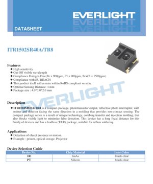
1. Product Overview
The ITR1502SR40A/TR8 is a highly integrated, surface-mount reflective photo interrupter designed for non-contact sensing applications. It combines an infrared emitter and a silicon phototransistor detector within a single, compact black clear lens package. The device is engineered for reliable object presence or motion detection with a specified optimal sensing distance of 4 mm. Its leadless package is specifically designed for compatibility with modern reflow soldering processes, making it suitable for high-volume automated assembly.
1.1 Core Features and Advantages
- High Sensitivity: The silicon phototransistor provides a strong electrical response to reflected infrared light, enabling reliable detection.
- Visible Light Cut-Off: The black clear lens material effectively blocks ambient visible light, minimizing the potential for false triggering from environmental light sources.
- Compact Form Factor: With dimensions of 4.0 mm x 3.0 mm x 2.0 mm, it is ideal for space-constrained PCB designs.
- Reflow Solderable: The leadless (Tape & Reel) package allows for standard SMT assembly, supporting peak soldering temperatures up to 260°C for 5 seconds.
- Environmental Compliance: The device is compliant with Halogen-Free standards (Br < 900ppm, Cl < 900ppm, Br+Cl < 1500ppm), EU REACH regulations, and is RoHS compliant.
- Long Focal Distance: For its package family, it offers a relatively long optimal sensing distance of 4 mm.
1.2 Target Market and Applications
This component is targeted at designers of consumer electronics, office automation, and industrial control systems requiring reliable, low-cost object sensing. Its primary function is to detect the presence, absence, or passage of an object without physical contact.
- Printers and Copiers: Detecting paper jams, tray status, or media presence.
- Optical Storage Drives (e.g., CD/DVD): Sensing disk tray position or detecting the presence of a disk.
- Projectors and Displays: Monitoring filter status, cover position, or other internal mechanisms.
- Vending Machines and Kiosks: Detecting product dispensing or user interaction.
- Home Appliances: Position sensing in smart locks, coffee makers, or other automated devices.
2. In-Depth Technical Parameter Analysis
The performance of the ITR1502SR40A/TR8 is defined by a comprehensive set of electrical and optical parameters. Understanding these is critical for proper circuit design and reliable system operation.
2.1 Absolute Maximum Ratings
These ratings define the stress limits beyond which permanent damage to the device may occur. Operation under these conditions is not guaranteed.
- Input Power Dissipation (Pd): 75 mW at or below 25°C free air temperature.
- Forward Current (IF): 50 mA (continuous).
- Peak Forward Current (IFP): 1 A for pulses ≤100μs at a 1% duty cycle.
- Reverse Voltage (VR): 5 V.
- Collector Power Dissipation (PC): 75 mW.
- Collector Current (IC): 25 mA.
- Collector-Emitter Voltage (VCEO): 30 V.
- Emitter-Collector Voltage (VECO): 5 V.
- Operating Temperature (Topr): -25°C to +85°C.
- Storage Temperature (Tstg): -40°C to +100°C.
- Lead Soldering Temperature: 260°C for 5 seconds (1/16 inch from the body).
2.2 Electro-Optical Characteristics (Ta=25°C)
These are the guaranteed performance parameters under specified test conditions.
Input (Infrared Emitter - IR GaAs Chip):
- Forward Voltage (VF): Typically 1.2V, maximum 1.4V at IF = 20 mA. This defines the voltage drop across the LED when driven.
- Reverse Current (IR): Maximum 10 μA at VR = 6V.
- Peak Wavelength (λP): 940 nm (nominal) at IF = 10 mA. This is in the near-infrared spectrum, invisible to the human eye.
Output (Phototransistor - Silicon Chip):
- Dark Current (ICEO): Typically 1 nA, maximum 100 nA at VCE = 20V. This is the leakage current when no light is incident on the detector.
- Transfer Characteristics - Collector Current (IC(ON)): Minimum 60 μA, typical, maximum 450 μA under test conditions: VCE=2V, IF=4mA, and a reflective target at d=4mm. This is the key parameter indicating sensitivity.
- Transfer Characteristics - Off-State Current (IC(OFF)): Maximum 600 nA under the same test conditions but with no reflection (or an absorbing target).
- Response Time (tr, tf): Typically 20 μs, maximum 100 μs for both rise and fall times. Tested at VCE=2V, IC=100μA, RL=1kΩ, d=4mm. This defines the switching speed.
Note: Operating dark current may be affected by the surrounding environment (e.g., ambient IR sources).
2.3 Bin Range of Collector Current
The devices are sorted (binned) based on their measured collector current (IC(ON)) under standard test conditions. This allows designers to select parts with consistent sensitivity for their application.
- Bin A: 60 μA ≤ IC(ON) < 120 μA
- Bin B: 100 μA ≤ IC(ON) < 220 μA
- Bin C: 180 μA ≤ IC(ON) < 350 μA
- Bin D: 310 μA ≤ IC(ON) ≤ 450 μA
3. Performance Curve Analysis
The provided characteristic curves offer valuable insight into device behavior under varying conditions, which is essential for robust system design.
3.1 Electrical Characteristics
Forward Current vs. Forward Voltage: This curve shows the typical IV characteristic of the infrared emitter LED. It is non-linear, similar to a standard diode. The typical forward voltage is around 1.2V at 20mA.
Forward Current vs. Collector Current: This is the transfer curve, showing how the phototransistor's output current (IC) increases with the input LED drive current (IF). The relationship is roughly linear in the operating region, demonstrating the device's gain.
Collector Current vs. Collector-Emitter Voltage: This family of curves shows IC at different IF levels (e.g., 5mA, 10mA, 20mA, 50mA) as VCE varies. It illustrates that the phototransistor acts as a current source; above a certain VCE (saturation voltage, typically low), IC is primarily determined by the incident light (and thus IF).
3.2 Temperature Characteristics
Forward Voltage vs. Ambient Temperature: The forward voltage of the LED has a negative temperature coefficient, decreasing slightly as temperature increases (from about 1.21V at -20°C to 1.16V at 80°C).
Relative Collector Current vs. Ambient Temperature: This is a critical curve. The collector current (sensitivity) decreases significantly as temperature rises. At 80°C, the relative output is only about 80% of its value at 25°C. This must be accounted for in designs operating at high temperatures to ensure sufficient signal margin.
Collector Dark Current vs. Ambient Temperature: Dark current increases exponentially with temperature (from ~0.1nA at -40°C to nearly 1000nA at 100°C). In high-temperature applications, this increased leakage can become a significant portion of the signal, potentially reducing the signal-to-noise ratio.
Power Dissipation vs. Ambient Temperature: This derating curve shows the maximum allowable power dissipation for the device decreases linearly as ambient temperature increases above 25°C, reaching 0 mW at 100°C.
3.3 Optical and Spatial Characteristics
Wavelength Spectrum: The relative radiant intensity curve shows the emitter's output is centered at 940 nm with a typical spectral width. The black clear lens effectively transmits this IR light while blocking shorter visible wavelengths.
Relative Collector Current vs. Z-Moving Distance (Mirror): This curve defines the sensing profile. The output current is highest when the reflective target is at the optimal distance (4mm). The signal falls off as the target moves closer or farther away, defining the practical sensing window. The curve is roughly Gaussian in shape.
Switching Time vs. Load Resistance: Both rise time (tr) and fall time (tf) increase with higher load resistance (RL). For fastest switching, a lower RL should be used, but this will also result in a lower output voltage swing. Designers must balance speed and signal level.
4. Mechanical and Package Information
4.1 Package Dimensions
The device has a compact, leadless surface-mount package measuring 4.0 mm in length, 3.0 mm in width, and 2.0 mm in height. Key dimensional notes include:
- All dimensions are in millimeters.
- Tolerances are ±0.1mm unless otherwise specified.
- Lead spacing is measured where the lead emerges from the package.
- Product mass is approximately 0.025 grams.
4.2 Recommended PCB Land Pattern
A recommended solder pad layout is provided to ensure reliable soldering and mechanical stability. A critical design rule is emphasized: the amount of solder must be carefully controlled to prevent solder wicking or leakage into the gap between the PCB and the housing body. Excessive solder in this area can create stress, impair functionality, or reduce long-term reliability. The pad design typically includes thermal relief connections and sufficient copper area for a strong bond.
4.3 Polarity and Orientation
The device has a marked orientation (typically a dot or a notch on the top surface) indicating Pin 1. The pinout is standard for such devices: the infrared emitter anode and cathode form one pair, and the phototransistor collector and emitter form the other. The datasheet diagram must be consulted for the exact pin assignment. Incorrect orientation will prevent the device from functioning.
5. Soldering, Assembly, and Storage Guidelines
5.1 Reflow Soldering Conditions
The ITR1502SR40A/TR8 is rated for lead-free (Pb-free) reflow soldering processes. A recommended temperature profile is provided, which typically includes:
- Preheat/Ramp-up: A controlled rise to activate flux.
- Soak Zone: A period at a temperature below the liquidus to ensure uniform heating.
- Reflow Zone: Peak temperature should not exceed 260°C, and the time above 240°C should be limited (e.g., 30-60 seconds).
- Cooling: A controlled cool-down period.
Critical Note: Reflow soldering should not be performed more than two times on the same device to avoid thermal stress damage to the internal components and molding compound.
5.2 Moisture Sensitivity and Storage (MSL 3)
The package is moisture sensitive. Adherence to the following procedures is necessary to prevent "popcorning" (package cracking due to vapor pressure during reflow).
- Unopened Bag Storage: Store at ≤30°C and ≤90% RH. Use within one year of shipment.
- After Bag Opening: Store at ≤30°C and ≤70% RH.
- Floor Life: Devices must be soldered within 168 hours (7 days) after the moisture barrier bag is opened.
- Baking: If the floor life is exceeded or the moisture indicator (desiccant) shows saturation, bake the devices at 60°C ±5°C for 24 hours before use to remove absorbed moisture.
6. Packaging and Ordering Information
6.1 Tape and Reel Specifications
The device is supplied in standard EIA-481 compliant tape and reel packaging for automated pick-and-place assembly.
- Packing Quantity: 800 pieces per reel.
- Reels per Carton: 38 reels per outer carton.
- Outer Carton Dimensions: 409 mm (A) x 245 mm (B) x 360 mm (C).
The reel has a specific orientation label indicating the progressive direction. Detailed reel dimensions (hub diameter, reel width, etc.) are provided for compatibility with placement equipment.
6.2 Packing Procedure
Reels are packaged in sealed aluminum moisture-proof bags. Each bag contains a desiccant pack and a humidity indicator card to monitor moisture levels. Multiple bags are then packed into a master shipping carton.
7. Application Design Considerations
7.1 Typical Application Circuit
A basic application circuit involves two main parts:
- Emitter Drive: A current-limiting resistor in series with the IR LED. The resistor value is calculated as Rlimit = (VCC - VF) / IF. For example, with a 5V supply and a desired IF of 20mA: Rlimit = (5V - 1.2V) / 0.02A = 190Ω (use a standard 200Ω resistor). The LED can be driven continuously or pulsed for lower power consumption.
- Detector Interface: The phototransistor is typically connected with a pull-up resistor (RL) from the collector to VCC. The emitter is connected to ground. With no reflected light, the transistor is off, and the output voltage at the collector is high (VCC). When light is detected, the transistor turns on, pulling the output voltage low towards ground. The value of RL affects both the output voltage swing and the response speed (see performance curves). A common value is 1kΩ to 10kΩ.
7.2 Design Factors for Reliable Sensing
- Target Reflectivity: The signal strength is directly proportional to the reflectivity of the target surface. A white, reflective surface will produce the strongest signal; a black, matte surface will produce the weakest. The system must be designed to work with the worst-case target.
- Target Distance and Alignment: The sensor has a specific "sweet spot" at 4mm. Variations in assembly tolerances or target position will affect the signal level. Design mechanical fixtures to maintain consistent alignment.
- Ambient Light Immunity: While the black lens blocks most visible light, strong sources of infrared light (sunlight, incandescent bulbs) can still cause interference. Using a modulated (pulsed) LED drive signal and synchronous detection in the receiver circuitry can greatly improve immunity to ambient light.
- Temperature Compensation: As shown in the curves, sensitivity drops with temperature. For applications operating over a wide temperature range, the circuit should include margin or active compensation (e.g., adjusting IF based on temperature) to ensure reliable detection at high temperatures.
- Electrical Noise: Keep sensor traces short and away from noisy digital or power lines. Use bypass capacitors near the device on both VCC and the LED supply if pulsed.
8. Technical Comparison and Differentiation
The ITR1502SR40A/TR8 differentiates itself in the market of reflective sensors through several key attributes:
- vs. Larger Through-Hole Interrupters: Its primary advantage is the ultra-compact 4.0x3.0mm SMD footprint, enabling miniaturization and automated assembly, which larger through-hole devices cannot match.
- vs. Other SMD Reflective Sensors: The combination of a 4mm optimal distance and a black clear lens for visible light blocking within this small form factor is a specific design point. Some competitors may offer shorter sensing distances or different lens materials.
- vs. Analog Output vs. Digital Sensors: This device provides an analog phototransistor output, giving the designer full control over the threshold and allowing for analog distance/reflectivity measurements. This offers more flexibility compared to sensors with built-in digital logic that simply provide a on/off signal.
- vs. Discrete Emitter/Detector Pairs: The integrated package ensures precise, fixed alignment between the emitter and detector, which is difficult and costly to achieve with two separate components. It also simplifies PCB layout and assembly.
9. Frequently Asked Questions (Based on Technical Parameters)
Q1: What is the difference between the bins (A, B, C, D)? How do I choose?
A: The bins represent different ranges of sensitivity (IC(ON)). Choose a bin based on your required signal margin. For applications with highly reflective targets or short distances, a lower bin (A or B) may suffice. For low-reflectivity targets, longer distances, or high-temperature operation where sensitivity drops, a higher bin (C or D) provides more headroom. Consistency within a bin is also important for production.
Q2: Can I drive the IR LED with a voltage directly without a current-limiting resistor?
A: No. The LED's forward voltage is not a fixed value and varies with temperature and device. Driving it directly from a voltage source will result in uncontrolled current, likely exceeding the Absolute Maximum Rating and destroying the emitter. Always use a series current-limiting resistor.
Q3: My sensor works erratically. What could be the cause?
A: Common issues include: 1) Insufficient signal margin: Check IC(ON) with your specific target and ensure it's well above your circuit's detection threshold, accounting for temperature derating. 2) Ambient light interference: Shield the sensor from direct bright light or implement modulation. 3) Solder joint issues: Verify the recommended land pattern was used and inspect for solder bridges or insufficient solder. 4) Excessive dark current: At very high temperatures, dark current can become significant; ensure your circuit can distinguish it from the true signal.
Q4: How do I calculate the power dissipation of the device?
A: Total power dissipation is the sum of the input (LED) and output (phototransistor) dissipation. PD(total) ≈ (VF * IF) + (VCE(sat) * IC). Under typical conditions (IF=20mA, VF=1.2V, IC=5mA, VCE=0.2V), PD ≈ 24mW + 1mW = 25mW, which is well below the 75mW rating at 25°C. Remember to derate this value if operating above 25°C.
10. Operational Principle
The ITR1502SR40A/TR8 operates on the principle of modulated light reflection. The internal infrared light-emitting diode (IR LED) emits light at a peak wavelength of 940 nm. This light travels out of the package through the lens, strikes a target object in front of the sensor, and is partially reflected back. The integrated silicon phototransistor, which is sensitive to infrared light, detects this reflected light. When photons strike the base region of the phototransistor, they generate electron-hole pairs, which act as a base current. This photogenerated base current is then amplified by the transistor's gain, resulting in a much larger collector current (IC). This collector current is the electrical output signal, which is proportional to the intensity of the reflected light. The black clear lens material is transparent to the 940 nm IR light but opaque to most visible light, providing immunity to ambient visible light sources. The fixed, co-planar alignment of the emitter and detector within the molded package creates a precise optical path optimized for detecting objects at a specific distance (4mm) in front of the sensor.
LED Specification Terminology
Complete explanation of LED technical terms
Photoelectric Performance
| Term | Unit/Representation | Simple Explanation | Why Important |
|---|---|---|---|
| Luminous Efficacy | lm/W (lumens per watt) | Light output per watt of electricity, higher means more energy efficient. | Directly determines energy efficiency grade and electricity cost. |
| Luminous Flux | lm (lumens) | Total light emitted by source, commonly called "brightness". | Determines if the light is bright enough. |
| Viewing Angle | ° (degrees), e.g., 120° | Angle where light intensity drops to half, determines beam width. | Affects illumination range and uniformity. |
| CCT (Color Temperature) | K (Kelvin), e.g., 2700K/6500K | Warmth/coolness of light, lower values yellowish/warm, higher whitish/cool. | Determines lighting atmosphere and suitable scenarios. |
| CRI / Ra | Unitless, 0–100 | Ability to render object colors accurately, Ra≥80 is good. | Affects color authenticity, used in high-demand places like malls, museums. |
| SDCM | MacAdam ellipse steps, e.g., "5-step" | Color consistency metric, smaller steps mean more consistent color. | Ensures uniform color across same batch of LEDs. |
| Dominant Wavelength | nm (nanometers), e.g., 620nm (red) | Wavelength corresponding to color of colored LEDs. | Determines hue of red, yellow, green monochrome LEDs. |
| Spectral Distribution | Wavelength vs intensity curve | Shows intensity distribution across wavelengths. | Affects color rendering and quality. |
Electrical Parameters
| Term | Symbol | Simple Explanation | Design Considerations |
|---|---|---|---|
| Forward Voltage | Vf | Minimum voltage to turn on LED, like "starting threshold". | Driver voltage must be ≥Vf, voltages add up for series LEDs. |
| Forward Current | If | Current value for normal LED operation. | Usually constant current drive, current determines brightness & lifespan. |
| Max Pulse Current | Ifp | Peak current tolerable for short periods, used for dimming or flashing. | Pulse width & duty cycle must be strictly controlled to avoid damage. |
| Reverse Voltage | Vr | Max reverse voltage LED can withstand, beyond may cause breakdown. | Circuit must prevent reverse connection or voltage spikes. |
| Thermal Resistance | Rth (°C/W) | Resistance to heat transfer from chip to solder, lower is better. | High thermal resistance requires stronger heat dissipation. |
| ESD Immunity | V (HBM), e.g., 1000V | Ability to withstand electrostatic discharge, higher means less vulnerable. | Anti-static measures needed in production, especially for sensitive LEDs. |
Thermal Management & Reliability
| Term | Key Metric | Simple Explanation | Impact |
|---|---|---|---|
| Junction Temperature | Tj (°C) | Actual operating temperature inside LED chip. | Every 10°C reduction may double lifespan; too high causes light decay, color shift. |
| Lumen Depreciation | L70 / L80 (hours) | Time for brightness to drop to 70% or 80% of initial. | Directly defines LED "service life". |
| Lumen Maintenance | % (e.g., 70%) | Percentage of brightness retained after time. | Indicates brightness retention over long-term use. |
| Color Shift | Δu′v′ or MacAdam ellipse | Degree of color change during use. | Affects color consistency in lighting scenes. |
| Thermal Aging | Material degradation | Deterioration due to long-term high temperature. | May cause brightness drop, color change, or open-circuit failure. |
Packaging & Materials
| Term | Common Types | Simple Explanation | Features & Applications |
|---|---|---|---|
| Package Type | EMC, PPA, Ceramic | Housing material protecting chip, providing optical/thermal interface. | EMC: good heat resistance, low cost; Ceramic: better heat dissipation, longer life. |
| Chip Structure | Front, Flip Chip | Chip electrode arrangement. | Flip chip: better heat dissipation, higher efficacy, for high-power. |
| Phosphor Coating | YAG, Silicate, Nitride | Covers blue chip, converts some to yellow/red, mixes to white. | Different phosphors affect efficacy, CCT, and CRI. |
| Lens/Optics | Flat, Microlens, TIR | Optical structure on surface controlling light distribution. | Determines viewing angle and light distribution curve. |
Quality Control & Binning
| Term | Binning Content | Simple Explanation | Purpose |
|---|---|---|---|
| Luminous Flux Bin | Code e.g., 2G, 2H | Grouped by brightness, each group has min/max lumen values. | Ensures uniform brightness in same batch. |
| Voltage Bin | Code e.g., 6W, 6X | Grouped by forward voltage range. | Facilitates driver matching, improves system efficiency. |
| Color Bin | 5-step MacAdam ellipse | Grouped by color coordinates, ensuring tight range. | Guarantees color consistency, avoids uneven color within fixture. |
| CCT Bin | 2700K, 3000K etc. | Grouped by CCT, each has corresponding coordinate range. | Meets different scene CCT requirements. |
Testing & Certification
| Term | Standard/Test | Simple Explanation | Significance |
|---|---|---|---|
| LM-80 | Lumen maintenance test | Long-term lighting at constant temperature, recording brightness decay. | Used to estimate LED life (with TM-21). |
| TM-21 | Life estimation standard | Estimates life under actual conditions based on LM-80 data. | Provides scientific life prediction. |
| IESNA | Illuminating Engineering Society | Covers optical, electrical, thermal test methods. | Industry-recognized test basis. |
| RoHS / REACH | Environmental certification | Ensures no harmful substances (lead, mercury). | Market access requirement internationally. |
| ENERGY STAR / DLC | Energy efficiency certification | Energy efficiency and performance certification for lighting. | Used in government procurement, subsidy programs, enhances competitiveness. |